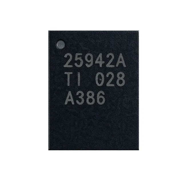
TPS25940ARVCR - 18V 5A eFuse with True Reverse Blocking | TI
MPN: TPS25940ARVCR ✓ Active| Qty | Unit Price | Extended |
|---|---|---|
| 1 | $1.45 | $1.45 |
| 10 | $1.31 | $13.10 |
| 100 | $1.12 | $112.00 |
| 500 | $0.96 | $480.00 |
| 1,000 | $0.84 | $840.00 |
| 3,000 | $0.72 | $2,160.00 |
TPS25940ARVCR Overview
An eFuse (electronic fuse) is a semiconductor protection device that combines the function of a traditional fuse, current-limiting circuit, and load switch into a single integrated circuit. It sits between a power source and a downstream load to provide inrush current limiting, overcurrent protection, short-circuit protection, reverse-current blocking, and often overvoltage/undervoltage protection. Unlike a one-time-use fuse, an eFuse can be reset by toggling its enable input. In the broader system hierarchy, an eFuse is a subcategory of hot-swap controller / power-distribution switch, which itself falls under power management IC and finally semiconductor device.
Key features include 2.7V to 18V operating input range, 0.6A to 5.2A programmable current limit (set via external resistor), ±8% ILIM accuracy over temperature, integrated true reverse-current blocking, programmable inrush current slew rate via dVdt pin, fault output (FLT) pin for system monitoring, thermal shutdown, and an EN/UVLO pin for precise turn-on control. The device supports the SATA DevSleep specification, drawing microamp-level quiescent current during sleep to meet SSD power budgets.
The TPS25940 family uses a charge-pump-driven N-channel MOSFET architecture with an integrated gate driver. The true reverse-current block comparator monitors VOUT versus VIN and disables the FET when VOUT > VIN, preventing discharge of downstream capacitance into the input rail. The DEVSLP pin activates a low-quiescent-current mode by disabling most internal circuits while keeping reverse-blocking monitoring active. The device operates from -40C to +85C ambient.
Typical applications include NVMe/SATA SSD power rails, USB Type-C VBUS hot-swap protection, multi-port USB hubs, fan protection circuits, and any 5V/12V rail that requires inrush control and disconnect on fault.
When designing with this eFuse, place the ILIM resistor close to the ILIM pin to minimize noise pickup, use a 1µF or larger input bulk capacitor to suppress voltage transients during hot-plug events, and observe absolute maximum VIN of 20V including transient ringing. The package's thermal pad must be soldered to a sufficiently large copper pour to handle steady-state I²R dissipation - at 5A continuous through 42mΩ, the part dissipates ~1.05W.
This page synthesizes distributor pricing, drop-in alternatives, and practical design notes not found on the manufacturer product page.
Drop-in alternatives for TPS25940ARVCR — same package, pin-to-pin compatible. Different-package parts requiring PCB rework are excluded.
Quick Comparison Tool — Select alternative parts for side-by-side comparison:
TPS25940ARVCT
📋 Reference alternative (not in catalog)
TPS25940ARVCRG4
📋 Reference alternative (not in catalog)
TPS25942ARVCR
📋 Reference alternative (not in catalog)
TPS25940ARVCR-Q1
📋 Reference alternative (not in catalog)
TPS25810TWRVCRQ1
📋 Reference alternative (not in catalog)
TPS2544RTER
📋 Reference alternative (not in catalog)
TPS25940ARVCR Specifications
| Product Type | Electronic Fuse (eFuse) / Hot-Swap Controller |
| Input Voltage Range | 2.7 V to 18 V |
| Absolute Maximum VIN | 20 V |
| On-Resistance (Rdson) | 42 mΩ (typical) |
| Programmable Current Limit Range | 0.6 A to 5.2 A |
| Maximum Continuous Load Current | 5.3 A |
| Current Limit Accuracy | ±8% over temperature |
| Reverse Current Blocking | True reverse-current block (integrated) |
| DevSleep Support | Yes (SATA DevSleep spec) |
| Inrush Slew Rate Control | Programmable via dVdt capacitor |
| Fault Output | Yes (FLT pin, open-drain) |
| Enable / UVLO | EN/UVLO pin, precision threshold |
| Thermal Shutdown | Yes |
| Operating Temperature Range | -40 C to +85 C |
| Package | WQFN-20 (RVC) 4x3 mm |
| Mounting Type | Surface Mount |
| RoHS Status | Compliant |
TPS25940ARVCR Pin Configuration
| Pin 1 | GND — Ground reference |
| Pin 2 | VIN — Input supply voltage (2.7 V to 18 V) |
| Pin 3 | dVdt — Slew-rate control capacitor pin |
| Pin 4 | ILIM — Current-limit set resistor to GND |
| Pin 5 | EN/UVLO — Enable and undervoltage lockout input |
| Pin 6 | FLT — Open-drain fault output |
| Pin 7 | DEVSLP — DevSleep mode enable input (active high) |
| Pin 8 | VOUT — Regulated output to load |
| Pin 9 | PGND — Power ground |
| Pin 10 | NC — Not connected (per datasheet) |
| Pin 11 | NC — Not connected (per datasheet) |
| Pin 12 | NC — Not connected (per datasheet) |
| Pin 13 | NC — Not connected (per datasheet) |
| Pin 14 | NC — Not connected (per datasheet) |
| Pin 15 | NC — Not connected (per datasheet) |
| Pin 16 | NC — Not connected (per datasheet) |
| Pin 17 | NC — Not connected (per datasheet) |
| Pin 18 | NC — Not connected (per datasheet) |
| Pin 19 | NC — Not connected (per datasheet) |
| Pin 20 | PGND — Exposed thermal pad / power ground |
Typical Applications
TPS25940ARVCR is suitable for 6 applications: SATA / NVMe SSD Power Path Protection, USB Type-C VBUS Hot-Swap Protection, Multi-Port USB Hub Downstream Protection, Fan and Motor Protection Circuit, Hot-Swap Insertion Card Power Management, Industrial 24V (12V) Load Switch with Fault Reporting.
SATA / NVMe SSD Power Path Protection
The TPS25940ARVCR is purpose-built for SATA and NVMe SSD power management. Its 2.7 V to 18 V input range covers 3.3 V and 5 V SSD rails, and the integrated SATA DevSleep pin support reduces quiescent current to single-digit microamps during sleep states - critical for meeting the SATA DevSleep specification that limits sleep-mode power to <5 mW. The 42 mΩ Rdson minimizes voltage drop at 3 A continuous load, preserving headroom for the SSD's downstream DC-DC converters. Reverse-current blocking prevents the SSD's bulk output capacitance from backfeeding the host rail during hot-unplug events, which would otherwise trigger host-side OVP faults.
Recommended
USB Type-C VBUS Hot-Swap Protection
In USB Type-C VBUS hot-swap paths, the TPS25940ARVCR serves as the in-line protection element between the connector and downstream circuitry. Its 18 V absolute-maximum rating tolerates the worst-case 20 V VBUS overshoot during PD negotiation transients, while the 2.7 V minimum allows operation on legacy 5 V Type-A ports through adapter cables. The programmable dVdt inrush control prevents large inrush currents that would otherwise collapse the VBUS rail during attach events. Compared to discrete Schottky + P-FET solutions, the TPS25940ARVCR achieves far lower conduction loss (42 mΩ vs typically 100 mΩ+) while integrating fault reporting via the FLT pin for the port manager.
Recommended
Multi-Port USB Hub Downstream Protection
For multi-port USB hubs, the TPS25940ARVCR provides per-port protection against overcurrent, short-circuit, and back-drive faults. Each downstream port sees a dedicated eFuse that isolates a faulty device from the upstream 5 V rail, preventing hub-wide brownouts. The FLT pin can be wire-OR'd to the hub controller for centralized fault monitoring. The 5.3 A current limit is well above the USB 3.0 spec's 900 mA per-port requirement while still protecting against sustained 5 A short events at the connector. Its small WQFN-20 4x3 mm footprint allows one eFuse per port to fit in space-constrained hub designs.
Recommended
Fan and Motor Protection Circuit
In 12 V brushless DC fan or small motor paths, the TPS25940ARVCR delivers both inrush limiting and stall-current protection. Brushless motor windings present a near-short at startup, and without slew-rate control the inrush can reach 10x steady-state current, tripping upstream fuses or collapsing the 12 V rail. The TPS25940ARVCR's programmable dVdt pin lets the designer slow the output rise to match the motor's time constant, while the 5.2 A current limit covers stall current of typical 12 V fans (1-3 A running, 3-5 A stalled). The FLT pin allows the system MCU to log fan-failure events.
Recommended
Hot-Swap Insertion Card Power Management
In PCI Express cards, PXI modules, and other plug-in-card architectures, the TPS25940ARVCR safely manages the inrush of board-decoupling capacitance during insertion. Without slew-rate control, the host backplane sees a multi-hundred-amp transient as the card's 100-1000 µF of bulk capacitance charges in microseconds. The TPS25940ARVCR's dVdt programming lets the designer slow this rise to 1-10 ms, limiting inrush to safe levels. Reverse-current blocking protects against cards that may backfeed through their on-card regulators during hot-removal, a common failure mode in modular systems.
Recommended
Industrial 24V (12V) Load Switch with Fault Reporting
In industrial 24 V (typically regulated to 12 V) sensor and actuator power distribution, the TPS25940ARVCR functions as a resettable electronic fuse with diagnostic feedback. Unlike a glass or PTC fuse, it can be reset via the EN pin after a fault clears, eliminating service visits in remote installations. The 0.6 A to 5.2 A programmable range covers a wide spectrum of industrial loads - from small sensor clusters (~0.5 A) to multi-solenoid actuators (~4 A). The open-drain FLT pin can drive an opto-isolator to signal fault status back to a PLC over an isolation barrier.
Recommended
Recommended Products Summary
Engineering reference data for TPS25940ARVCR — comparison, design guidance, and compliance information.
Selection Guide
Comparison with Alternatives
| Parameter | This Product | TPS25940ARVCT | TPS25940ARVCRG4 | TPS25942ARVCR | TPS25810TWRVCRQ1 | TPS2544RTER |
|---|---|---|---|---|---|---|
| Brand | Texas Instruments | Texas Instruments | Texas Instruments | Texas Instruments | Texas Instruments | Texas Instruments |
| Package | WQFN-20 (RVC) 4x3 mm | WQFN-20 (RVC) 4x3 mm | WQFN-20 (RVC) 4x3 mm | WQFN-20 (RVC) 4x3 mm | WQFN-20 (RVC) 4x3 mm | WQFN-16 (RTE) - different footprint |
| Input Voltage Range | 2.7 V to 18 V | 2.7 V to 18 V | 2.7 V to 18 V | 2.7 V to 18 V | 4.5 V to 18 V | 4.5 V to 5.5 V |
| Reverse Current Blocking | Yes (true reverse block) | Yes | Yes | Yes | Yes | No (USB switch only) |
| DevSleep Support | Yes | Yes | Yes | Yes | No | No |
| Operating Temperature | -40 C to +85 C | -40 C to +85 C | -40 C to +85 C | -40 C to +85 C | -40 C to +125 C (AEC-Q100) | -40 C to +85 C |
| Approx. Unit Price (USD) | $1.45 (qty 1) | ~$1.45 (qty 1) | ~$1.45 (qty 1) | ~$1.55 (qty 1) | ~$1.85 (qty 1, automotive) | ~$1.10 (qty 1) |
Key Differentiators
- True reverse-current blocking with sub-microsecond response (vs TPS2544RTER)
- SATA DevSleep support with microamp-level quiescent current (vs TPS2544RTER)
- Wide 2.7 V to 18 V input range covers both 5 V and 12 V rails (vs TPS2544RTER)
- Higher 5.2 A programmable current limit vs USB-spec 3 A (vs TPS2544RTER)
Design Notes
Estimated: At 5 A continuous through the 42 mΩ internal FET, the TPS25940ARVCR dissipates approximately 5² × 0.042 = 1.05 W. With a typical WQFN-20 (RVC) 4x3 mm board-mount thermal resistance of around 45 C/W on a 4-layer PCB with 1 oz copper and modest thermal pad coverage, junction temperature rise above ambient is roughly 47 C - so at 85 C ambient, Tj approaches 132 C. For sustained 5 A operation, expand the exposed-pad copper pour to at least 1 cm² per side and add thermal vias to inner planes to drop θJA below 35 C/W. If the load is intermittent (typical SSD duty cycle), no heatsink is required.
Place the ILIM resistor (RILIM) directly adjacent to the ILIM pin and route its GND end to the device's PGND pin with a short, wide trace - any series inductance or ground noise will degrade current-limit accuracy. The dVdt capacitor sets the output slew rate via C = I_ILIM × t_rise / V_OUT; a 10 nF cap on dVdt yields roughly 1 ms rise time at 5 V output, which is appropriate for most SSD and USB loads. Add a 1 µF X7R minimum bulk capacitor on VOUT close to the device to suppress transient ringing during FET turn-on.
Do not exceed the 20 V absolute-maximum VIN rating, even briefly - USB PD negotiation transients at 20 V VBUS can clip the input and damage the internal charge pump. Add a TVS diode (e.g., SMBJ18A) on VIN for Type-C applications. The DEVSLP pin must be tied high or low; floating it can leave the device in an undefined state. Avoid running the FLT pin below the rated pull-up voltage (5.5 V max) - exceeding this can back-power the internal ESD structure and damage the device.
Use a star-ground topology: route the analog ground (GND pin) and the power-return (PGND/exposed pad) on separate pours that join only at the device's PGND pin. This prevents high-current load transients from coupling into the ILIM resistor ground and shifting the current-limit threshold. Place input and output capacitors, the ILIM resistor, and the dVdt capacitor on the same PCB layer as the device with short, wide traces - via transitions on power paths add inductance that causes voltage spikes during hot-plug events.
Compliance Information
RoHS and REACH compliance per TI product page. AEC-Q100 qualified automotive variant is TPS25940ARVCR-Q1 (separate part number). Standard TPS25940ARVCR is for industrial/consumer use.







