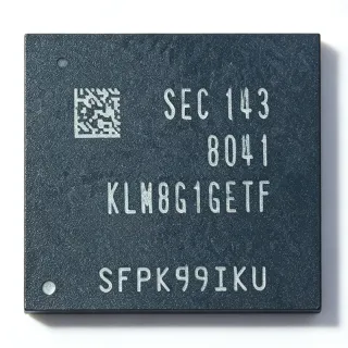
W9751G6NB-25 - 512Mb DDR2-800 SDRAM x16 | Winbond
MPN: W9751G6NB-25 ✓ Active| Qty | Unit Price | Extended |
|---|---|---|
| 1 | $7.05 | $7.05 |
| 10 | $6.7 | $67.00 |
| 100 | $6.35 | $635.00 |
| 500 | $5.95 | $2,975.00 |
| 1,000 | $5.6 | $5,600.00 |
W9751G6NB-25 Overview
DDR2 SDRAM (Double Data Rate 2 Synchronous Dynamic Random Access Memory) is a type of volatile semiconductor memory that transfers data on both the rising and falling edges of the clock signal, doubling effective bandwidth compared to single data rate SDRAM. Within the memory hierarchy, DDR2 SDRAM sits below DDR3 and DDR4 in performance but remains widely used in cost-sensitive embedded systems. The broader taxonomy runs: DDR2 SDRAM -> SDRAM -> DRAM -> semiconductor memory -> memory IC.
Key features of the W9751G6NB-25 include an auto precharge function for simplified memory controller operation, a data mask (DM) function for selective byte writes, and dynamic on-chip termination (ODT) that improves signal integrity at high data rates by terminating the bus at the die rather than on the motherboard. These on-die features reduce external component count and strengthen signal integrity in dense PCB layouts.
Technically, the device achieves transfer rates up to DDR2-800 with the -25 speed grade suffix, operating from a 1.8 V supply per the DDR2 JEDEC standard. Winbond sorts the W9751G6NB family into speed grades -18, -25, and -3 (with I and J industrial variants), allowing designers to scale performance within an identical footprint. The 84-ball VFBGA ball map follows the standard DDR2 x16 JEDEC footprint, ensuring controller and PCB compatibility across the family.
Typical applications include embedded computing boards, industrial PCs, networking equipment, set-top boxes, and legacy desktop/laptop memory module repair where DDR2 is still required. The x16 organization suits low-cost controllers with narrower 16-bit buses, and its proven presence in systems such as the Dell Latitude D630 demonstrates field reliability.
A key design consideration: DDR2 termination must follow the dynamic ODT settings in the Winbond datasheet, and VREF rails require clean, low-noise routing for timing margins to hold across the full 0 to 85 C commercial temperature range.
This page synthesizes distributor pricing, drop-in alternatives, and practical design notes not found in the manufacturer datasheet.
Drop-in alternatives for W9751G6NB-25 — same package, pin-to-pin compatible. Different-package parts requiring PCB rework are excluded.
Variants in this series
Same-series models that are drop-in compatible with W9751G6NB-25 (same form factor and footprint) — differing in Data Rate, Organization.
Quick Comparison Tool — Select alternative parts for side-by-side comparison:
W9751G6NB25I
✅ Drop-In📋 Reference alternative (not in catalog)
W9751G6NB-3
✅ Drop-In ⚠️ 参数待验证📋 Reference alternative (not in catalog)
W9751G6NB-18
✅ Drop-In ⚠️ 参数待验证📋 Reference alternative (not in catalog)
W9725G6KB-25
✅ Drop-In📋 Reference alternative (not in catalog)
W9725G6KB-25I
✅ Drop-In ⚠️ 参数待验证📋 Reference alternative (not in catalog)
W9751G6NB-25 Maximum Ratings & Electrical Characteristics
| Memory Type | SDRAM - DDR2 |
| Memory Size | 512 Mbit |
| Organization | 32M x 16 (8M words x 4 banks x 16 bits) |
| Interface | Parallel |
| Clock Frequency | 400 MHz |
| Data Rate | DDR2-800 (800 Mbps/pin) |
| Access Time | 57.5 ns |
| Supply Voltage | 1.8 V |
| Package | 84-VFBGA (8 x 12.5 mm) |
| Operating Temperature | 0C to +85C |
| Auto Precharge | Yes |
| Data Mask Function | Yes |
| On-Die Termination | Dynamic ODT |
| Family Speed Grades | -18, -25, -3 (with I/J industrial variants) |
| Mounting Type | Surface Mount |
W9751G6NB-25 84-vfbga (8 x 12.5 mm) Pin Configuration Guide
Pin configuration for W9751G6NB-25 (84-vfbga (8 x 12.5 mm) package). This digital IC includes GPIO, communication interfaces (UART, SPI, I2C), and power pins. Refer to the manufacturer datasheet for alternate pin functions and configuration options. Essential for embedded system design and PCB layout.

No detailed pinout data available for W9751G6NB-25.
Refer to the datasheet for full pin configuration.
Typical Applications
W9751G6NB-25 is suitable for 6 applications: Embedded Industrial PCs, Networking Equipment, Set-Top Boxes and Consumer Media Devices, Legacy Computer Memory Repair, Test and Measurement Instrumentation, Automotive Infotainment (Aftermarket).
Embedded Industrial PCs
Industrial PC mainboards and single-board computers frequently specify DDR2 x16 SDRAM in 84-VFBGA footprints, and the W9751G6NB-25 fits these sockets directly. Its 512 Mbit density at 32M x 16 organization supports 1 GB configurations with two devices on a 32-bit bus, adequate for Windows XP/embedded Linux workloads. Dynamic ODT terminates the address/data bus at the die, easing routing on 4-6 layer industrial PCBs without external termination resistor packs. The DDR2-800, 400 MHz clock rate pairs with common embedded chipsets, and auto precharge offloads controller scheduling. For deployments below 0C or above +85C, the drop-in industrial variant W9751G6NB25I covers the same footprint.
Recommended
Networking Equipment
Switch, router, and gateway line cards use DDR2 SDRAM for packet buffering and routing tables, where the W9751G6NB-25's 400 MHz DDR2-800 interface supplies 1.6 GB/s peak bandwidth per device in a 16-bit configuration. The data mask (DM) function allows the network processor to write partial cachelines without read-modify-write cycles, improving buffer management efficiency. Dynamic on-chip termination improves eye margins on longer bus runs typical of line-card layouts. The compact 84-VFBGA (8 x 12.5 mm) body suits dense card designs where component height below 1.2 mm is required. Auto precharge simplifies burst transfers common in packet forwarding engines.
Recommended
Set-Top Boxes and Consumer Media Devices
Set-top box and digital media SoCs of the DDR2 generation pair naturally with the W9751G6NB-25: a single 512 Mbit x16 device provides 64 MB of system memory, and two devices deliver 128 MB for Linux-based UI stacks. The 1.8 V supply keeps power consumption low for always-on consumer devices, while the 84-VFBGA package withstands lead-free reflow profiles used in high-volume consumer assembly. DDR2-800 bandwidth sustains video decode frame buffers, and dynamic ODT reduces BOM cost by eliminating external termination networks. Cost-sensitive designs benefit from the -25 speed grade pricing versus faster -3 parts when the SoC clocks at or below 400 MHz.
Recommended
Legacy Computer Memory Repair
Service depots repairing DDR2-era systems, such as the Dell Latitude D630, use the W9751G6NB-25 as a pin-for-pin replacement for the W9725G6KB-25 on memory modules and motherboards. Field reports confirm successful installations without BIOS tweaks or memory recalibration because both parts share the DDR2-800, 512 Mbit x16, 84-VFBGA specification set. The 57.5 ns access time and standard JEDEC DDR2 timing registers ensure the platform's SPD-driven initialization works unchanged. Technicians should confirm the platform's 400 MHz memory clock and 0 to +85 C ambient suitability, selecting the industrial W9751G6NB25I for extended-temperature embedded repairs.
Recommended
Test and Measurement Instrumentation
Bench instruments, data loggers, and modular chassis of the DDR2 generation buffer measurement data in DDR2 SDRAM, and the W9751G6NB-25 provides a cost-effective 512 Mbit x16 buffer with 1.6 GB/s peak throughput at DDR2-800. The auto precharge function simplifies FPGA-based memory controllers, which dominate instrument logic, by folding precharge commands into read/write bursts. Dynamic ODT maintains signal integrity across the longer traces typical of instrument backplanes, and the data mask enables efficient sample-stream writes. The 84-VFBGA package's 8 x 12.5 mm footprint fits standard instrumentation board outlines and reflow assembly processes.
Recommended
Automotive Infotainment (Aftermarket)
Aftermarket head units, navigation boxes, and telematics retrofits built on DDR2-era SoCs use the W9751G6NB-25 for 64-128 MB of application memory in a footprint that survives automotive vibration profiles thanks to the lead-free VFBGA solder-ball attach. The 1.8 V rail simplifies power-tree design from 5 V or battery inputs, and DDR2-800 bandwidth supports map rendering and media decode frame buffers. Designers should validate the commercial 0 to +85 C range against the product's thermal spec, choosing the W9751G6NB25I industrial variant where cabin temperatures exceed commercial limits. Dynamic ODT eases routing on high-density infotainment PCBs.
Recommended
Recommended Products Summary
Engineering reference data for W9751G6NB-25 — comparison, design guidance, and compliance information.
Selection Guide
Comparison with Alternatives
| Parameter | This Product | W9751G6NB25I | W9751G6NB-3 | W9751G6NB-18 | W9725G6KB-25 | W9725G6KB-25I |
|---|---|---|---|---|---|---|
| Package | 84-VFBGA (8 x 12.5 mm) | 84-VFBGA (8 x 12.5 mm) - same | 84-VFBGA (8 x 12.5 mm) - same | 84-VFBGA (8 x 12.5 mm) - same | 84-VFBGA (8 x 12.5 mm) - same | 84-VFBGA (8 x 12.5 mm) - same |
| Brand | Winbond Electronics | Winbond Electronics | Winbond Electronics | Winbond Electronics | Winbond Electronics | Winbond Electronics |
| Memory Size | 512 Mbit | 512 Mbit | 512 Mbit | 512 Mbit | 512 Mbit | 512 Mbit |
| Organization | 32M x 16 | 32M x 16 | 32M x 16 | 32M x 16 | 32M x 16 | 32M x 16 |
| Data Rate / Clock | DDR2-800 / 400 MHz | DDR2-800 / 400 MHz | DDR2-1066 / 533 MHz | DDR2-800 (faster-timing grade) | DDR2-800 / 400 MHz | DDR2-800 / 400 MHz |
| Supply Voltage | 1.8 V | 1.8 V | 1.8 V | 1.8 V | 1.8 V | 1.8 V |
| On-Die Termination | Dynamic ODT | Dynamic ODT | Dynamic ODT | Dynamic ODT | Dynamic ODT | Dynamic ODT |
Key Differentiators
- Lowest-cost DDR2-800 speed grade in the family (vs W9751G6NB-3)
- Field-proven pin-for-pin repair substitution (vs W9725G6KB-25)
- Industrial temperature path without redesign (vs W9751G6NB25I)
Design Notes
Configure dynamic ODT via the EMRS registers per the Winbond W9751G6NB datasheet before enabling full-speed DDR2-800 operation. Because termination sits on the die, route data groups as short as practical (target under 50 mm) and keep DQS/DQS# as tightly coupled length-matched pairs within 25 mils of skew to DQ bytes. Validate eye diagrams at 400 MHz with the controller's drive strength settings; dynamic ODT removes external resistor packs but does not forgive excessive stubs or via discontinuities on 4-layer boards.
The W9751G6NB-25 operates from a 1.8 V VDD/VDDQ rail per the DDR2 standard. Estimated: at DDR2-800 with typical activity, a single 512 Mbit x16 device draws several hundred milliwatts; budget the 1.8 V regulator with at least 30-50% margin over your worst-case measured current and place bulk (100 uF) plus per-ball-region 0.1 uF decoupling close to the VDD/VDDQ ball clusters. Keep VREF quiet: route it as a separate filtered node (resistor divider or dedicated reference output) with local 0.1 uF and 1 uF capacitors, since VREF noise directly erodes timing margins.
The 84-VFBGA (8 x 12.5 mm) uses a fine ball pitch requiring PCB escape routing; define fanout escape patterns before placement to avoid asymmetrical trace lengths. Fly-by or balanced-tree address/command topology is preferred per DDR2 practice; keep clock (CK/CK#) length-matched to address/command within specification and length-match DQS strobes per byte lane. Confirm the reflow profile suits VFBGA ball composition (lead-free SAC alloys) and inspect ball collapse with X-ray on first articles, since hidden balls make rework difficult.
Do not mix commercial (-25) and industrial (-25I) temperature grades on the same bus without verifying identical AC timing tables in the datasheet; although pin-compatible, register settings and ODT values should be confirmed per device. Also confirm the memory controller supports the -25 speed grade timing (DDR2-800 CL5/CAS latency per Winbond datasheet) - substituting a faster -3 grade is always safe, but running the -25 above its rated 400 MHz clock violates specification and causes data corruption.
Compliance Information
Per Winbond's published purchasing guide, all Winbond Flash/DRAM products ship in RoHS-compliant packaging and current W9751G6NB production is halogen-free. REACH and conflict-minerals status should be confirmed via Winbond's official product compliance documentation.