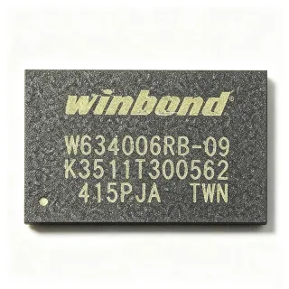
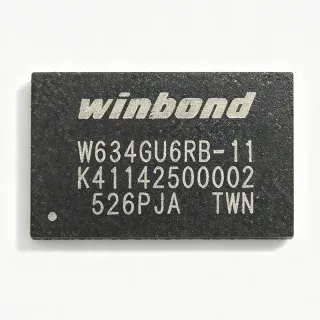
W9825G6KH-6-TR - 256Mbit SDRAM 166MHz TSOP II | Winbond
MPN: W9825G6KH-6-TR ✓ Active| Qty | Unit Price | Extended |
|---|---|---|
| 1 | $0.35 | $0.35 |
| 10 | $0.31 | $3.10 |
| 100 | $0.24 | $24.00 |
| 500 | $0.17 | $85.00 |
| 1,000 | $0.12 | $120.00 |
W9825G6KH-6-TR Overview
Synchronous DRAM is a class of dynamic random-access memory that interfaces with a system clock signal, allowing burst transfers that are far faster than asynchronous DRAM or SRAM at comparable cost per bit. Within the memory hierarchy, the W9825G6KH sits below caches (SRAM) and above mass storage, serving as main working memory in embedded systems. It is internally organized as four banks of 4M x 16 bits, using 13 row and 9 column address lines multiplexed on shared A0-A12 pins.
Key features include a parallel x16 data interface, LSAMR mode register programming for burst length and CAS latency configuration, separate LDQM/UDQM data masks for byte-level write control, and clock enable (CKE) for low-power power-down modes. The -6 speed grade delivers a data bandwidth of up to 200M words per second per the manufacturer datasheet, and the device is sorted into speed grades -5, -5I, -6, -6I, -6J, -6L, -75, 75J and 75L for PC-industrial-standard compliance.
The device is fabricated in a mature DRAM process and uses standard SDRAM command sets: ACTIVE, READ, WRITE, PRECHARGE, AUTO REFRESH, and SELF REFRESH. Refresh is required every 64 ms across 8192 rows, with auto-refresh handled by the memory controller. The 3.3V supply keeps power consumption compatible with legacy embedded processors, and TSOP II lead-frame construction supports standard reflow assembly.
Typical applications include main memory for ARM Cortex-M7 and other MCU/MPU boards with SDRAM controllers, industrial HMI and display frame buffers, network appliances, and test instrumentation requiring 32 MB of working RAM.
Design consideration: budget a complete refresh window in the memory controller; refresh commands consume roughly 1-2% of bandwidth at 64 ms intervals, which matters for deterministic real-time workloads.
This page adds distributor pricing, drop-in speed-grade and cross-organization alternatives, and controller-configuration design notes not found in the manufacturer datasheet alone.
Drop-in alternatives for W9825G6KH-6-TR — same package, pin-to-pin compatible. Different-package parts requiring PCB rework are excluded.
Quick Comparison Tool — Select alternative parts for side-by-side comparison:
W9825G6KH-6I
✅ Drop-In📋 Reference alternative (not in catalog)
W9825G6KH-5
✅ Drop-In ⚠️ 参数待验证📋 Reference alternative (not in catalog)
W9825G6KH-75
✅ Drop-In ⚠️ 参数待验证📋 Reference alternative (not in catalog)
W9825G6KH-6J
✅ Drop-In📋 Reference alternative (not in catalog)
W9825G6JB-6-TR
✅ Drop-In📋 Reference alternative (not in catalog)
W9825G6KH-6-TR Maximum Ratings & Electrical Characteristics
| Memory Type | SDRAM - SDR Synchronous DRAM |
| Memory Capacity | 256 Mbit (32 MB) |
| Organization | 16M x 16 |
| Bank Architecture | 4 banks x 4M x 16 |
| Interface | Parallel |
| Supply Voltage | 3.3 V |
| Maximum Clock Frequency | 166 MHz |
| Clock Cycle Time | 5 ns |
| Row Address Lines | A0-A12 (13-bit) |
| Column Address Lines | A0-A8 (9-bit) |
| Data Mask | LDQM / UDQM (byte masking) |
| Refresh Interval | 64 ms (8192 rows) |
| Operating Temperature | 0C to +70C (commercial grade) |
| Package | 54-TSOP II |
| Mounting Type | Surface Mount |
| Packaging | Tape & Reel (TR) |
| Speed Grades Available | -5, -5I, -6, -6I, -6J, -6L, -75, 75J, 75L |
W9825G6KH-6-TR 54-tsop ii Pin Configuration Guide
Pin configuration for W9825G6KH-6-TR (54-tsop ii package). This digital IC includes GPIO, communication interfaces (UART, SPI, I2C), and power pins. Refer to the manufacturer datasheet for alternate pin functions and configuration options. Essential for embedded system design and PCB layout.

No detailed pinout data available for W9825G6KH-6-TR.
Refer to the datasheet for full pin configuration.
Typical Applications
W9825G6KH-6-TR is suitable for 6 applications: Embedded MCU/MPU Main Memory, Industrial HMI and Display Frame Buffer, Networking and Communication Equipment, Test and Measurement Instrumentation, Audio Processing and Effect Systems, FPGA-Based Embedded Systems.
Embedded MCU/MPU Main Memory
The W9825G6KH-6-TR serves as external working RAM for ARM Cortex-M7, Cortex-A, and legacy MCU boards equipped with SDRAM controllers (e.g., STM32 FMC). Its 16M x 16 organization matches the common 16-bit FMC configuration with 13-row and 9-column addressing, and 32 MB capacity is sufficient for RTOS heaps, TCP/IP stacks, and application buffers. Running at 3.3V with CAS latency 3 at 166 MHz, it delivers burst bandwidth far above asynchronous SRAM at a fraction of the cost per megabyte. Place the device close to the controller with matched-length traces on the clock and address bus; a single 0.1uF decoupling capacitor per supply pin plus bulk capacitance is standard practice.
Recommended
Industrial HMI and Display Frame Buffer
Industrial human-machine interface panels use the W9825G6KH-6-TR as a frame buffer for TFT LCD controllers. A 800x480 RGB565 frame occupies about 750 KB, so 32 MB holds multiple full-frame buffers plus a graphics layer, enabling double-buffered tear-free rendering. The x16 parallel bus feeds common LCD/TFT controller ICs directly, and the 166 MHz -6 grade sustains the read bandwidth needed for 60 fps refresh at moderate resolutions. Self-refresh mode allows the CPU to enter low-power states between UI updates, an important benefit in battery-backed operator terminals. Commercial temperature range suits indoor panel installations; select the -6I for outdoor or unheated cabinets.
Recommended
Networking and Communication Equipment
Routers, switches, and industrial gateways use the W9825G6KH-6-TR for packet buffers and descriptor rings. The 4-bank architecture allows interleaved bank access, hiding row-activation latency during sequential packet processing, and byte-level LDQM/UDQM masking supports efficient variable-length buffer management. At 166 MHz the bus provides ample headroom for 100 Mbps line-rate forwarding with dual frame buffers per port. The mature 3.3V interface integrates cleanly with legacy network processor and FPGA designs still common in industrial Ethernet equipment. Designers should size refresh overhead (about 1-2% of bandwidth) into worst-case latency calculations for deterministic packet handling.
Recommended
Test and Measurement Instrumentation
Bench instruments, data loggers, and oscilloscope front ends use the W9825G6KH-6-TR to hold acquisition records and waveform memory. The 32 MB capacity stores millions of 16-bit samples, and the deterministic SDRAM command protocol lets FPGA-based acquisition engines stream data at bus rate with predictable timing. AUTO REFRESH scheduling must be coordinated with the acquisition state machine so refresh cycles do not create dead time during triggered capture; CKE power-down conserves power between measurements. Commercial-grade parts suit benchtop environments, while portable field instruments should specify the industrial -6I variant for -40C to +85C confidence.
Recommended
Audio Processing and Effect Systems
Professional audio effects, mixers, and DSP-based processors use the W9825G6KH-6-TR for delay lines, reverb buffers, and multitrack scratch memory. A one-second stereo 48 kHz 24-bit delay requires under 350 KB, so 32 MB supports long reverbs and multiple simultaneous effect channels with wide margin. The x16 bus interfaces directly to DSP external memory ports or FPGA memory controllers, and consistent bank interleaving minimizes latency jitter, which is critical for audio path determinism. Because SDRAM adds refresh cycles, buffer controllers should budget worst-case access time to avoid buffer underruns in the audio interrupt service routine.
Recommended
FPGA-Based Embedded Systems
FPGA designs employ the W9825G6KH-6-TR as soft-processor main memory (MicroBlaze, Nios II) and as video or DSP data buffering. FPGA vendor memory controllers are pre-configured for 3.3V SDR SDRAM with 16M x 16 x 4-bank geometry, making integration straightforward: map 13 row, 9 column address bits and set CAS latency 3 within the -6 timing window. The 54-TSOP II package solders onto standard two- and four-layer boards with fly-by or star address routing. Designers should verify mode register programming sequences in simulation, since incorrect MRS setup during initialization is the most common bring-up failure.
Recommended
Recommended Products Summary
Engineering reference data for W9825G6KH-6-TR — comparison, design guidance, and compliance information.
Selection Guide
Comparison with Alternatives
| Parameter | This Product | W9825G6KH-6I | W9825G6KH-5 | W9825G6KH-75 | W9825G6JB-6-TR |
|---|---|---|---|---|---|
| Package | 54-TSOP II | 54-TSOP II - same | 54-TSOP II - same | 54-TSOP II - same | 54-TSOP II - same |
| Brand | Winbond Electronics | Winbond Electronics | Winbond Electronics | Winbond Electronics | Winbond Electronics |
| Capacity | 256 Mbit | 256 Mbit | 256 Mbit | 256 Mbit | 256 Mbit |
| Organization | 16M x 16 | 16M x 16 | 16M x 16 | 16M x 16 | 32M x 8 |
| Max Clock Frequency | 166 MHz | 166 MHz | 200 MHz | 133 MHz | 166 MHz |
| Operating Temperature | 0C to +70C | -40C to +85C | 0C to +70C | 0C to +70C | 0C to +70C |
| Supply Voltage | 3.3 V | 3.3 V | 3.3 V | 3.3 V | 3.3 V |
| Controller Change Required | n/a (reference) | None - identical | None - timing compatible (faster) | Reduce clock to 133 MHz | Reconfigure to x8 width, 10-bit columns |
Key Differentiators
- Cost per megabyte leader in SDR SDRAM class (vs W9825G6KH-6I)
- 166 MHz speed with drop-in faster option (vs W9825G6KH-75)
- 16-bit bus for maximum bandwidth per pin (vs W9825G6JB-6-TR)
Design Notes
Route the SDRAM clock with series termination (22-33 ohm) and keep CLK-to-address/command trace skew within the datasheet tAC/DH/DS budget. On two-layer boards keep total bus length under roughly 100 mm and add a solid ground return under the bus. Match all DQ lines to similar lengths to avoid intra-byte skew at 166 MHz. These are board-level estimates - validate with the Winbond datasheet timing tables at your actual clock rate and temperature.
Provide one 0.1uF ceramic capacitor per supply pin pair plus at least 10uF bulk capacitance near the device. DRAM core current spikes on row activation; separating VDD/VDDQ planes or at least filtering VDDQ locally reduces noise coupling into the analog domain. Estimated: at 166 MHz with continuous burst activity, current draw is typically in the tens of milliamps range - consult the datasheet IDD tables for exact operating-current conditions rather than sizing rails from estimates.
The most frequent bring-up failure is incorrect mode register programming: issue the MRS command after a 100 us power-up wait and at least one AUTO REFRESH, per the standard SDRAM initialization sequence. Second, configure the controller for exactly 13 row x 9 column x 4 bank geometry - mistuned addressing silently wraps memory. Third, honor the 64 ms/8192-row refresh requirement; halving refresh rate may pass at room temperature but corrupts data at elevated temperature. Verify all sequences against the manufacturer datasheet.
Compliance Information
Compliance data was not present in the provided web data. Verify RoHS/REACH status on the official Winbond product page or distributor compliance certificates before procurement.