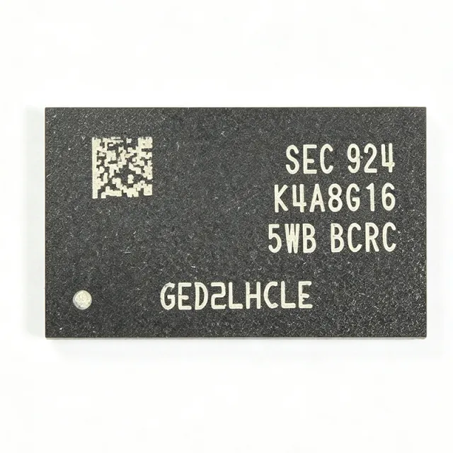
K4A8G165WB-BCRC - 8Gb DDR4 SDRAM x16 2400Mbps | Samsung
MPN: K4A8G165WB-BCRC ✓ Active| Qty | Unit Price | Extended |
|---|---|---|
| 1 | $15.47 | $15.47 |
| 10 | $14.7 | $147.00 |
| 100 | $13.92 | $1,392.00 |
| 500 | $13.23 | $6,615.00 |
| 1,000 | $12.57 | $12,570.00 |
K4A8G165WB-BCRC Overview
DDR4 SDRAM (fourth-generation Double Data Rate Synchronous Dynamic Random-Access Memory) is the industry-standard volatile DRAM technology for computing and embedded systems. It transfers data on both clock edges and operates at 1.2V versus DDR3's 1.5V, cutting core power by roughly 25% while raising bandwidth. Within the memory hierarchy it sits as the main-system-memory tier: DRAM -> DDR4 SDRAM -> volatile memory -> semiconductor memory.
Key features of the -BCRC speed grade include 2400 Mbps operation at CL17-class timings, an operating temperature range of -40C to +95C, on-die termination (ODT), dynamic ODT, ZQ calibration, auto-precharge, an asynchronous reset input, and CRC and CA parity support for link integrity. The x16 organization provides a wide 16-bit data bus, maximizing bandwidth per chip and simplifying single-chip designs.
Technically, the device uses Samsung's 8Gb B-die monolithic DRAM process with CMOS core logic. Bank-group architecture enables fast back-to-back accesses, while programmable read/write latencies and refresh modes (auto-refresh and self-refresh) let the memory controller optimize for latency or power. The fine-pitch FBGA-96 package (0.8 mm ball pitch) delivers short, controlled-impedance interconnects for signal integrity at 1200 MHz clock rates.
Typical applications include server and data-center memory subsystems, industrial PCs and control systems, network routers and switches, and automotive-adjacent infotainment and connectivity platforms.
Design consideration: maintain a stable 1.14V-1.26V supply with dense decoupling near the power balls and follow the datasheet fly-by routing and VREF guidelines to pass eye-mask compliance at 2400 Mbps.
This page synthesizes distributor pricing, drop-in alternatives within the Samsung K4A8G165WB family, and practical design notes not found in the manufacturer datasheet.
Drop-in alternatives for K4A8G165WB-BCRC — same package, pin-to-pin compatible. Different-package parts requiring PCB rework are excluded.
Variants in this series
Same-series models that are drop-in compatible with K4A8G165WB-BCRC (same form factor and footprint) — differing in Package, Data Rate, Operating Temperature, Interface, Burst Length.
Quick Comparison Tool — Select alternative parts for side-by-side comparison:
K4A8G165WB-BCPB
✅ Drop-In✓ In Stock
$2.3 / Unit
View Datasheet →K4A8G165WB-BCTD
✅ Drop-In✓ In Stock
$37 / Unit
View Datasheet →K4A8G165WB-BCWE
✅ Drop-In✓ In Stock
$6.55 / Unit
View Datasheet →K4A8G165WB-BIWE
✅ Drop-In✓ In Stock
$14.22 / Unit
View Datasheet →K4A8G165WC-BCRC
✅ Drop-In✓ In Stock
$23 / Unit
View Datasheet →K4A8G165WB-BIRC
✅ Drop-In✓ In Stock
$39.5 / Unit
View Datasheet →K4A8G165WB-BCRC Maximum Ratings & Electrical Characteristics
| Memory Type | DDR4 SDRAM (DRAM, volatile) |
| Memory Size | 8 Gb (1 GB) |
| Memory Organization | 512M x 16 |
| Data Rate | 2400 Mbps (PC4-19200) |
| Supply Voltage | 1.2 V (1.14 V to 1.26 V) |
| Technology | CMOS DRAM, Samsung 8Gb B-die |
| Package | 96-ball FBGA (PBGA96) |
| Ball Pitch | 0.8 mm |
| Mounting Type | Surface Mount |
| Operating Temperature | -40C to +95C |
| Interface | DDR4 (Double Data Rate, synchronous) |
| On-Die Termination | Yes (ODT with dynamic ODT) |
| ZQ Calibration | Yes |
| CRC / CA Parity | Yes (CRC function) |
| Auto Precharge | Yes |
| Asynchronous Reset | Yes |
| Refresh | Auto-refresh and self-refresh |
| RoHS Status | Compliant |
K4A8G165WB-BCRC 96-ball fbga (pbga96) Pin Configuration Guide
Pin configuration for K4A8G165WB-BCRC (96-ball fbga (pbga96) package). This digital IC includes GPIO, communication interfaces (UART, SPI, I2C), and power pins. Refer to the manufacturer datasheet for alternate pin functions and configuration options. Essential for embedded system design and PCB layout.

No detailed pinout data available for K4A8G165WB-BCRC.
Refer to the datasheet for full pin configuration.
Typical Applications
K4A8G165WB-BCRC is suitable for 6 applications: Server and Data Center Memory, Industrial Control Systems, Network Routers and Switches, Automotive Infotainment and Connectivity, High-Performance Embedded Computing, Test and Measurement Instruments.
Server and Data Center Memory
In server and data-center platforms, the K4A8G165WB-BCRC provides 8Gb density per chip with a wide 16-bit bus, letting designers scale total memory capacity with fewer devices than x8 parts. Its 2400 Mbps data rate (PC4-19200) supplies substantial bandwidth per chip for virtualization and cloud workloads, while CRC and CA parity on the command/address bus protect link integrity in electrically noisy server backplanes. The 1.2V operation reduces per-GB power versus DDR3, an important metric in data centers where memory can be 30-40% of system power. On-die termination with dynamic ODT simplifies multi-rank fly-by topologies used in registered DIMMs and memory mezzanines.
Recommended
Industrial Control Systems
Industrial PCs, PLCs, and motion controllers use the K4A8G165WB-BCRC for its -40C to +95C operating range, which covers unconditioned factory-floor cabinets and outdoor enclosures. The 512M x 16 organization delivers 1 GB of main memory in a single 96-ball FBGA, valuable in compact fanless controllers where board area is constrained. Its 2400 Mbps rate supports real-time HMI rendering and data logging, while self-refresh mode preserves memory contents in low-power standby, a common industrial requirement. For designs that must survive harsher thermal environments, the pin-compatible K4A8G165WB-BIRC industrial-grade variant enables BOM reuse without PCB changes.
Recommended
Network Routers and Switches
Networking equipment exploits the K4A8G165WB-BCRC's high bandwidth-to-chip ratio: one device delivers 16-bit-wide DDR4-2400 traffic for packet buffers, route tables, and queue descriptors. The x16 organization halves chip count versus x8 for the same bus width, reducing routing complexity on dense line-card designs. CRC and CA parity guard command/address integrity, and asynchronous reset supports fast line-card re-initialization after fault events. With 8Gb per package, designs can provision deep buffering for bursty traffic without exhausting board space, and the 1.2V core helps meet thermal budgets in sealed switch chassis with limited airflow.
Recommended
Automotive Infotainment and Connectivity
Automotive infotainment head units, digital cockpits, and telematics gateways require DRAM that operates reliably from cold crank to full solar load; the K4A8G165WB-BCRC's -40C to +95C rating addresses this window. Its 2400 Mbps bandwidth supports HD navigation rendering, camera input processing, and concurrent media playback, while 8Gb density accommodates multi-display frame buffers. The 1.2V rail integrates cleanly with automotive PMIC DDR4 supplies, and ODT with ZQ calibration maintains signal integrity over temperature drift. For applications requiring formal automotive qualification documentation, Samsung offers automotive-grade DDR4 variants; confirm grade requirements with your component engineering team.
Recommended
High-Performance Embedded Computing
Embedded compute modules such as COM Express, SMARC, and custom SoM designs use the K4A8G165WB-BCRC where x16 DDR4 simplifies layout: the 16-bit bus needs only one chip per channel instead of two x8 devices, shrinking package height and total BOM. The 96-ball FBGA with 0.8 mm pitch is reflow-compatible with standard SMT processes, and 8Gb per package reaches 2 GB or 4 GB on a small footprint using stacked placements. Programmable latencies let the design tune for latency-sensitive control planes, and the B-die's proven silicon maturity lowers qualification risk for long-lifecycle embedded programs requiring multi-year supply.
Recommended
Test and Measurement Instruments
Oscilloscopes, logic analyzers, and signal generators demand large, fast acquisition memories; the K4A8G165WB-BCRC's 8Gb capacity and 2400 Mbps interface support deep waveform capture and high-throughput streaming to processing engines. The x16 organization enables wide interleaved memory banks built from few chips, and CRC/CA parity protects long acquisition runs from link errors. Self-refresh supports persistent setup storage across power cycles, and the -40C to +95C range suits portable instruments used outdoors or in vehicles. Designers should follow the datasheet fly-by routing rules and length-match DQS/DQ groups to hold the 2400 Mbps eye margin on multilayer instrument boards.
Recommended
Recommended Products Summary
Engineering reference data for K4A8G165WB-BCRC — comparison, design guidance, and compliance information.
Selection Guide
Comparison with Alternatives
| Parameter | This Product | K4A8G165WB-BCPB | K4A8G165WB-BCTD | K4A8G165WC-BCRC | K4A8G165WB-BIRC |
|---|---|---|---|---|---|
| Package | 96-ball FBGA (PBGA96) | 96-ball FBGA - same | 96-ball FBGA - same | 96-ball FBGA - same | 96-ball FBGA - same |
| Brand | Samsung Electronics | Samsung Electronics | Samsung Electronics | Samsung Electronics | Samsung Electronics |
| Memory Size | 8 Gb | 8 Gb | 8 Gb | 8 Gb | 8 Gb |
| Data Rate | 2400 Mbps | 2133 Mbps | 2666 Mbps | 2400 Mbps | 2400 Mbps |
| Organization | 512M x 16 | 512M x 16 | 512M x 16 | 512M x 16 | 512M x 16 |
| Supply Voltage | 1.2 V (1.14-1.26 V) | 1.2 V | 1.2 V | 1.2 V | 1.2 V |
| Die Revision | B-die (WB) | B-die (WB) | B-die (WB) | C-die (WC) | B-die (WB) |
| Temperature Grade | -40C to +95C (C = commercial/extended) | Commercial grade | Commercial grade | Commercial grade | Industrial grade (BI) |
Key Differentiators
- Higher speed grade at identical pinout (vs K4A8G165WB-BCPB)
- Mature B-die silicon for long-lifecycle designs (vs K4A8G165WC-BCRC)
- Wider 16-bit bus halves chip count (vs K4A8G085WB-BCRC (x8 variant))
Design Notes
Route DDR4 address/command/control signals in fly-by topology with per-device on-die termination (ODT), matching the K4A8G165WB-BCRC datasheet layout guidelines. Keep DQS/DQS# and their associated DQ byte lanes length-matched within the datasheet skew budget; at 2400 Mbps the setup/hold margins shrink to a few hundred picoseconds, so a 2 mm mismatch can fail eye-mask compliance. Maintain a solid reference plane under all DDR4 nets and avoid routing over plane splits.
Supply the device with a stable 1.2V rail within the 1.14V-1.26V tolerance. Estimated decoupling guideline: place at least one 0.1 uF ceramic capacitor per two power/ground ball pairs within 2 mm of the package, plus bulk 10 uF per device and a low-ESR capacitor at VREF. Concurrent switching of 16 DQ lines causes di/dt spikes; insufficient decoupling appears as jitter on strobe alignment and refresh-related errors.
Do not omit the ZQ calibration resistor (RZQ, typically 240 ohm to ground per the datasheet); improper ZQ placement corrupts output driver and ODT impedance calibration. Connect the asynchronous reset ball to a known state at power-up, and honor the controller's initialization sequence (200 us stable clock, reset, CKE) before issuing commands. When swapping to the C-die K4A8G165WC-BCRC or a different speed grade, re-run read/write margin training on the SoC.
Compliance Information
RoHS compliant and lead-free per Samsung product documentation and distributor listings. Not an AEC-Q100 dedicated automotive-qualified grade; verify automotive requirements with Samsung.


