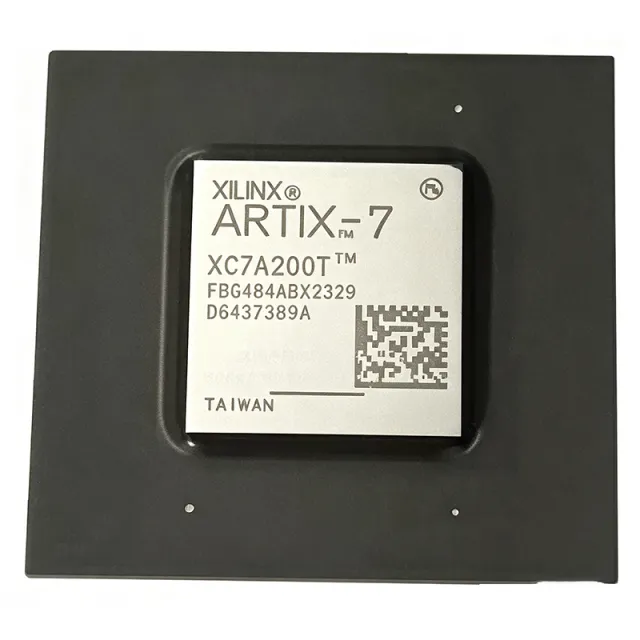
XC7A200T-2FBG484C - Artix-7 FPGA 740K Logic Cells | AMD Xilinx
MPN: XC7A200T-2FBG484C ✓ Active| Qty | Unit Price | Extended |
|---|---|---|
| 1 | $450 | $450.00 |
| 10 | $420 | $4,200.00 |
| 100 | $380 | $38,000.00 |
| 500 | $350 | $175,000.00 |
| 1,000 | $320 | $320,000.00 |
XC7A200T-2FBG484C Overview
An FPGA (Field-Programmable Gate Array) is an integrated circuit that can be configured by the customer or designer after manufacturing. It consists of programmable logic blocks, configurable interconnects, and I/O blocks, allowing for flexible implementation of digital circuits. FPGAs sit within the broader category of programmable logic devices (PLDs), which are part of the semiconductor industry. They are used in applications requiring parallel processing, high-speed I/O, and reconfigurable logic, such as communications, industrial automation, and aerospace.
Key features of the XC7A200T-2FBG484C include 740K logic cells, 215K logic slices, 13 Mb of block RAM, 740 DSP slices, and 10.3 Mb of distributed RAM. It also features 16 GTX transceivers supporting up to 6.6 Gbps, 10 clock management tiles (CMTs), and 285 user I/O pins. The device supports multiple I/O standards including LVCMOS, LVDS, and HSTL, and includes hardened memory controllers for DDR3 and DDR4.
The Artix-7 architecture is built on a 28nm high-k metal gate (HKMG) process, offering a balance of performance, power, and cost. The device includes advanced clocking resources, such as PLLs and MMCMs, and supports partial reconfiguration for dynamic logic updates. The 484-ball FBGA package provides a compact footprint with excellent thermal and electrical characteristics, enabling high-density designs.
Typical applications include software-defined radio (SDR), medical imaging, motor control, and high-performance computing. The high logic density and DSP slices make it ideal for signal processing, while the GTX transceivers support high-speed serial communication in networking and video applications.
When designing with this FPGA, careful attention must be paid to power supply decoupling and thermal management. The device requires multiple supply rails (VCCINT, VCCAUX, VCCO) and a proper power-up sequence. Use the Xilinx Power Estimator (XPE) to calculate power consumption and design an appropriate thermal solution.
This page synthesizes distributor pricing, drop-in alternatives, and practical design notes not found in the AMD Xilinx datasheet, providing a comprehensive resource for engineers.
Drop-in alternatives for XC7A200T-2FBG484C — same package, pin-to-pin compatible. Different-package parts requiring PCB rework are excluded.
Variants in this series
Same-series models that are drop-in compatible with XC7A200T-2FBG484C (same form factor and footprint) — differing in Operating Temperature, Package.
Quick Comparison Tool — Select alternative parts for side-by-side comparison:
XC7A200T-2FBG484I
✓ In Stock
$89.15 / Unit
View Datasheet →XC7A200T-1FBG484C
📋 Reference alternative (not in catalog)
XC7A200T-3FBG484C
📋 Reference alternative (not in catalog)
XC7A200T-2FBG484C Maximum Ratings & Electrical Characteristics
| Family | Artix-7 |
| Logic Cells | 740K |
| Logic Slices | 215K |
| Block RAM | 13 Mb |
| Distributed RAM | 10.3 Mb |
| DSP Slices | 740 |
| GTX Transceivers | 16 (up to 6.6 Gbps) |
| Clock Management Tiles | 10 |
| User I/O Pins | 285 |
| Core Voltage | 1.0V |
| I/O Standards | LVCMOS, LVDS, HSTL, etc. |
| Package | FBGA-484 |
| Operating Temperature | 0C to +85C |
| Speed Grade | -2 |
| RoHS Status | Compliant |
XC7A200T-2FBG484C Pin Configuration
| Pin A1 | IO_L1P_T0 — User I/O, differential pair P |
| Pin A2 | IO_L1N_T0 — User I/O, differential pair N |
| Pin B1 | IO_L2P_T0 — User I/O, differential pair P |
| Pin B2 | IO_L2N_T0 — User I/O, differential pair N |
| Pin C1 | VCCINT — Core voltage 1.0V |
| Pin C2 | GND — Ground |
| Pin D1 | VCCAUX — Auxiliary voltage 1.8V |
| Pin D2 | VCCO_0 — I/O bank 0 supply |
| Pin E1 | IO_L3P_T0 — User I/O, differential pair P |
| Pin E2 | IO_L3N_T0 — User I/O, differential pair N |
| Pin F1 | IO_L4P_T0 — User I/O, differential pair P |
| Pin F2 | IO_L4N_T0 — User I/O, differential pair N |
Typical Applications
XC7A200T-2FBG484C is suitable for 6 applications: Software-Defined Radio (SDR), Medical Imaging, Motor Control, High-Performance Computing (HPC), Video Processing, Aerospace and Defense.
Software-Defined Radio (SDR)
The XC7A200T-2FBG484C is ideal for SDR applications due to its high DSP slice count (740) and 16 GTX transceivers. The DSP slices enable efficient implementation of digital down/up converters, filters, and FFTs, while the transceivers support high-speed ADC/DAC interfaces. Its logic capacity allows for complex modulation schemes. In a typical SDR, the FPGA interfaces with RF front-end ADCs and DACs, performing real-time signal processing such as channelization, demodulation, and error correction. The GTX transceivers can connect to high-speed data converters (e.g., JESD204B) at up to 6.6 Gbps, ensuring low-latency data transfer. The device's 13 Mb of block RAM provides ample buffering for multi-channel processing. Performance considerations include managing power consumption, which can be optimized by using clock gating and dynamic reconfiguration. The FPGA's reconfigurability allows over-the-air updates to support new waveforms, making it a flexible platform for military and commercial communications.
Recommended
Medical Imaging
The XC7A200T-2FBG484C is well-suited for medical imaging systems such as ultrasound and CT scanners, where high-speed signal processing and parallel computation are required. Its 740 DSP slices can implement beamforming algorithms, image filtering, and reconstruction in real time. The 13 Mb of block RAM supports large image buffers, and the 285 I/O pins interface with multiple sensor arrays and display controllers. In an ultrasound system, the FPGA processes raw transducer data, performing quadrature demodulation, envelope detection, and scan conversion. The GTX transceivers can stream processed images to host processors or displays. The device's low power consumption (compared to larger FPGAs) is beneficial for portable or cart-based systems. Performance considerations include meeting real-time processing deadlines, which can be achieved by pipelining and parallel processing. The FPGA's reconfigurability allows algorithm updates without hardware changes, extending product lifespan.
Recommended
Motor Control
The XC7A200T-2FBG484C is used in advanced motor control systems for industrial automation and robotics. Its high logic density and DSP slices enable implementation of complex control algorithms such as field-oriented control (FOC) and direct torque control (DTC). The FPGA can handle multiple motor axes simultaneously, with each axis requiring PWM generation, current sensing, and encoder feedback processing. The 285 I/O pins connect to gate drivers, current sensors, and encoders. The device's deterministic timing ensures precise PWM signals, reducing torque ripple and improving efficiency. In a typical servo drive, the FPGA reads encoder signals, computes position and speed, and generates PWM outputs with dead-time compensation. The GTX transceivers can interface with industrial Ethernet protocols like EtherCAT for real-time communication. Performance considerations include managing switching frequencies and ensuring low latency in the control loop. The FPGA's parallel processing allows multiple control loops to run concurrently, improving system responsiveness.
Recommended
High-Performance Computing (HPC)
The XC7A200T-2FBG484C is used in HPC applications for accelerating compute-intensive tasks such as financial modeling, genomics, and scientific simulations. Its 740 DSP slices and 13 Mb of block RAM enable efficient implementation of custom arithmetic units and data pipelines. The FPGA can be programmed to perform parallel operations on large datasets, offloading work from CPUs. In a financial trading system, the FPGA can process market data feeds, calculate risk metrics, and execute trades with microsecond latency. The GTX transceivers support high-speed network interfaces (e.g., 10GbE) for data ingestion. The device's reconfigurability allows algorithm updates without hardware changes. Performance considerations include optimizing data movement between the FPGA and host processor, often using PCIe interfaces. The FPGA's low latency and high throughput make it ideal for real-time analytics and edge computing.
Recommended
Video Processing
The XC7A200T-2FBG484C is used in video processing systems for applications such as broadcast, surveillance, and medical imaging. Its high logic density and DSP slices enable real-time video scaling, color space conversion, and compression. The 13 Mb of block RAM supports line buffers and frame stores, while the 285 I/O pins interface with video codecs and display controllers. In a video surveillance system, the FPGA can process multiple camera streams, performing motion detection and object tracking. The GTX transceivers support high-speed serial interfaces like SDI for video transport. The device's parallel processing allows multiple video channels to be processed simultaneously. Performance considerations include meeting frame rate requirements (e.g., 60 fps) and managing bandwidth. The FPGA's reconfigurability allows support for new video standards (e.g., H.265) through firmware updates.
Recommended
Aerospace and Defense
The XC7A200T-2FBG484C is used in aerospace and defense systems for radar, electronic warfare, and secure communications. Its high logic density and DSP slices enable implementation of complex signal processing algorithms such as pulse compression, beamforming, and encryption. The 16 GTX transceivers support high-speed data links for radar and communication systems. The device's radiation-tolerant variants (not this specific part) are available for space applications, but this commercial version is suitable for ground-based and airborne systems. In a radar system, the FPGA processes received signals, performing matched filtering and target detection. The GTX transceivers can interface with high-speed ADCs and DACs. The device's reconfigurability allows mission-specific updates. Performance considerations include meeting real-time processing deadlines and ensuring reliability in harsh environments. The FPGA's low power consumption is beneficial for airborne platforms.
Recommended
Recommended Products Summary
Engineering reference data for XC7A200T-2FBG484C — comparison, design guidance, and compliance information.
Selection Guide
Comparison with Alternatives
| Parameter | This Product | XC7A200T-1FBG484C | XC7A200T-2FBG484I | XC7A200T-3FBG484C |
|---|---|---|---|---|
| Package | FBGA-484 | FBGA-484 - same | FBGA-484 - same | FBGA-484 - same |
| Logic Cells | 740K | 740K | 740K | 740K |
| Block RAM | 13 Mb | 13 Mb | 13 Mb | 13 Mb |
| DSP Slices | 740 | 740 | 740 | 740 |
| GTX Transceivers | 16 | 16 | 16 | 16 |
| User I/O Pins | 285 | 285 | 285 | 285 |
| Speed Grade | -2 | -1 | -2 | -3 |
| Temperature Range | 0C to +85C | 0C to +85C | -40C to +100C | 0C to +85C |
Key Differentiators
- Higher speed grade than XC7A200T-1FBG484C (vs XC7A200T-1FBG484C)
- Commercial temperature range vs industrial (vs XC7A200T-2FBG484I)
- Balanced speed grade vs XC7A200T-3FBG484C (vs XC7A200T-3FBG484C)
Design Notes
The XC7A200T-2FBG484C requires multiple power rails: VCCINT at 1.0V, VCCAUX at 1.8V, and VCCO for each I/O bank (1.2V to 3.3V). Use low-dropout regulators or DC-DC converters with adequate current capability. Decouple each power pin with 0.1uF and 10uF capacitors. Follow the power-up sequence specified in the datasheet: VCCINT, then VCCAUX, then VCCO.
The FBG484 package has a theta_JA of approximately 10.5 C/W. For a typical design consuming 10W, the junction temperature rise is 105C above ambient. Ensure adequate airflow or a heatsink to keep junction temperature below 85C for commercial grade. Use the Xilinx Power Estimator (XPE) to calculate power dissipation and design the thermal solution.
For high-speed GTX transceivers, use controlled impedance traces (e.g., 100 ohm differential) and minimize via stubs. Place decoupling capacitors close to the FPGA power pins. For DDR3 interfaces, follow the layout guidelines in the Artix-7 PCB design guide, including matched trace lengths and proper termination.
Compliance Information
RoHS compliant per AMD Xilinx product documentation. Other compliance details not specified in the provided data.
