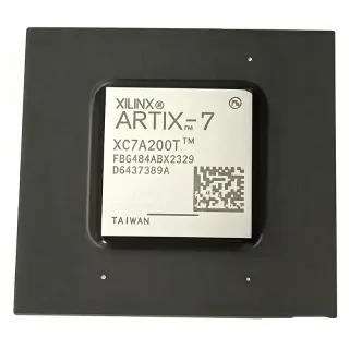
A3P1000-2FGG484M - ProASIC3 FPGA 1.5V 300 I/O | Microchip
MPN: A3P1000-2FGG484M ✓ Active| Qty | Unit Price | Extended |
|---|---|---|
| 1 | $116.55 | $116.55 |
| 10 | $107.43 | $1,074.30 |
| 100 | $94.21 | $9,421.00 |
| 500 | $84.72 | $42,360.00 |
| 1,000 | $75.44 | $75,440.00 |
A3P1000-2FGG484M Overview
A field programmable gate array (FPGA) is an integrated circuit that can be configured by the customer after manufacturing to implement custom digital logic. Unlike MCUs, FPGAs provide massive parallel processing and reconfigurable hardware. The ProASIC3 family uses flash-based switches, providing instant-on, low-power, secure, and radiation-tolerant operation. Within the product hierarchy, ProASIC3 sits in the mid-density segment between small CPLDs and high-end SRAM FPGAs, targeting industrial, aerospace, and communication applications.
Key features of the A3P1000-2FGG484M include a proprietary flash-based FPGA fabric with abundant system gates, 300 I/Os supporting multiple voltage standards, 147,456 bits of in-system programmable flash memory, and four I/O banks. The -2 speed grade offers balanced performance for logic-intensive designs, while the 1.5 V core reduces dynamic power. The 484-ball FBGA package provides a compact footprint with excellent routing flexibility.
From an architecture standpoint, the ProASIC3 device employs a fine-grained flash-based switch network, giving predictable timing without external boot memories. The device supports partial reconfiguration, secure bitstream protection, and live at power-up. Flash technology enables single-chip operation, reducing BOM cost and electromagnetic interference. The FPGA is programmed via JTAG using Microchip's FlashPro software, and supports industry-standard design flows.
Typical applications include industrial automation controllers, aerospace sensor processing, secure communication systems, medical imaging front-ends, and test-and-measurement instrumentation. The wide operating temperature option of this MPN (0C to +85C per distributor data) suits commercial equipment, while the same package accommodates industrial and military temperature variants for extended environments.
When designing with the A3P1000-2FGG484M, provide adequate decoupling on all 1.5 V core and I/O supply pins, and follow Microchip's power-up sequencing guidelines. The flash-based nature eliminates configuration time, but care must be taken with I/O bank assignments to match voltage standards.
This page synthesizes distributor pricing, drop-in alternatives, and practical design notes that are not typically compiled from the manufacturer datasheet, giving engineers a single-point reference for the A3P1000-2FGG484M.
Drop-in alternatives for A3P1000-2FGG484M — same package, pin-to-pin compatible. Different-package parts requiring PCB rework are excluded.
Variants in this series
Same-series models that are drop-in compatible with A3P1000-2FGG484M (same form factor and footprint) — differing in Operating Temperature, Package, System Gates, Family, Configuration Memory.
Quick Comparison Tool — Select alternative parts for side-by-side comparison:
A3P1000-2FGG484I
✅ Drop-In ⚠️ Specs Unverified📋 Reference alternative (not in catalog)
A3P1000-2FGG484
✅ Drop-In ⚠️ Specs Unverified📋 Reference alternative (not in catalog)
A3P1000-2FG484M
✅ Drop-In ⚠️ Specs Unverified✓ In Stock
$40.5 / Unit
View Datasheet →A3P1000-1FGG484I
✅ Drop-In ⚠️ Specs Unverified📋 Reference alternative (not in catalog)
A3P1000-1FGG484
✅ Drop-In ⚠️ Specs Unverified📋 Reference alternative (not in catalog)
A3P1000L-1FGG484I
✅ Drop-In✓ In Stock
$28.8 / Unit
View Datasheet →A3P1000-2FGG484M Maximum Ratings & Electrical Characteristics
| Product Type | FPGA - Field Programmable Gate Array |
| Series | ProASIC3 |
| Number of Logic Elements | 11000 LE |
| Number of User I/Os | 300 |
| RAM Bits | 147456 |
| Core Supply Voltage | 1.5 V |
| Minimum Operating Temperature | 0 C |
| Maximum Operating Temperature | +85 C |
| Mounting Style | SMD/SMT |
| Package / Case | FBGA-484 |
| Packaging | Tray |
| Number of I/O Banks | 4 |
| Speed Grade | -2 |
| Programming Interface | JTAG |
| Configuration Memory | Flash-based (non-volatile) |
A3P1000-2FGG484M fbga-484 Pin Configuration Guide
Pin configuration for A3P1000-2FGG484M (fbga-484 package). This digital IC includes GPIO, communication interfaces (UART, SPI, I2C), and power pins. Refer to the manufacturer datasheet for alternate pin functions and configuration options. Essential for embedded system design and PCB layout.

No detailed pinout data available for A3P1000-2FGG484M.
Refer to the datasheet for full pin configuration.
Typical Applications
A3P1000-2FGG484M is suitable for 6 applications: Industrial Automation and Control, Aerospace and Defense, Communication and Networking Equipment, Medical Electronics, Automotive Infotainment and Body Electronics, IoT Gateways and Edge Processing.
Industrial Automation and Control
The A3P1000-2FGG484M fits industrial automation designs that require high-speed parallel logic, deterministic real-time response, and non-volatile instant-on operation. With 11,000 logic elements and 300 user I/Os, it can implement multiple motor-control loops, high-speed counters, and fieldbus bridging in a single chip. The 1.5 V core reduces dynamic power, simplifying thermal management in sealed controllers. Because the device is flash-based, it powers up immediately without external configuration load, avoiding boot delays in safety-critical machinery. Programmers can use Microchip's FlashPro to update logic in the field over JTAG while preserving secure bitstream protection.
Recommended
Aerospace and Defense
In aerospace and defense, the A3P1000-2FGG484M's military temperature range and flash-based architecture provide inherent radiation tolerance, secure bitstream storage, and single-chip reliability. The 147,456 RAM bits and 300 I/Os support sensor interfacing, telemetry encoding, and custom encryption engines. Flash-based FPGAs are less susceptible to configuration upsets than SRAM-based parts, making them attractive for manned and unmanned platforms. Designers can use the device for avionics data concentration, deterministic control, or mission-record functions while taking advantage of the small FBGA footprint for weight-constrained boards.
Recommended
Communication and Networking Equipment
For communication systems, the A3P1000-2FGG484M offers high I/O count and predictable timing for protocol bridging, framing, and line-side processing. Its 300 user I/Os can connect directly to various PHY devices, parallel busses, and SDRAM. The non-volatile configuration eliminates boot time, enabling immediate link synchronization after power-up. The 1.5 V core helps minimize power consumption in rack-mounted equipment where thermal budgets are tight. Designers can implement MAC engines, packet classification, or queue managers using microcontrollers or soft processors, with the FPGA handling parallel data-path functions.
Recommended
Medical Electronics
The A3P1000-2FGG484M can implement medical imaging front-end logic, patient monitoring interfaces, and high-speed data acquisition. The 11K logic elements are sufficient for digital filtering, image preprocessing, and real-time alarm algorithms, while 300 I/Os allow connection to multi-channel ADCs and displays. The single-chip flash architecture improves system reliability and simplifies certification documentation. Low dynamic power helps meet strict thermal and EMC requirements in compact medical instruments. The device supports secure field updates, enabling post-market feature enhancements without hardware changes. Designers can leverage Microchip's IP cores for control and communication while keeping the FPGA at the center of the data path.
Recommended
Automotive Infotainment and Body Electronics
The A3P1000-2FGG484M can serve automotive infotainment bridging, sensor fusion preprocessing, or body-control logic, with its non-volatile configuration providing instant-on behavior for in-vehicle networks. The 1.5 V core and flash-based architecture reduce quiescent power, important for always-on modules. 300 I/Os support connectivity to displays, CAN/LIN transceivers, and external memory. While this MPN is listed with commercial temperature range in distributor data, the ProASIC3 family also offers industrial and automotive-qualified variants, so designers should choose the appropriate temperature grade variant for the target environment.
Recommended
IoT Gateways and Edge Processing
For IoT gateways and edge devices, the A3P1000-2FGG484M provides reconfigurable hardware acceleration for protocol conversion, sensor aggregation, and low-latency decision making. The flash-based FPGA wakes instantly and retains configuration without an external SPI flash, reducing BOM cost and attack surface. Its 147,456 bits of RAM buffer packets and telemetry data, while the 300 I/Os interface to multiple sensor buses. Although an FPGA is overkill for simple edge nodes, it shines when deterministic parallel operation is needed alongside a host processor. The 1.5 V core keeps power low enough for fanless enclosures.
Recommended
Recommended Products Summary
Engineering reference data for A3P1000-2FGG484M — comparison, design guidance, and compliance information.
Selection Guide
Comparison with Alternatives
| Parameter | This Product | A3P1000-2FGG484I | A3P1000-1FGG484I | A3P1000L-1FGG484I |
|---|---|---|---|---|
| Package | FBGA-484 | FBGA-484 | FBGA-484 | FBGA-484 |
| Brand | Microchip Technology | Microchip Technology | Microchip Technology | Microchip Technology |
| Logic Elements | 11000 LE | 11000 LE | 11000 LE | 11000 LE |
| User I/Os | 300 | 300 | 300 | 300 |
| RAM Bits | 147456 | 147456 | 147456 | 147456 |
| Core Supply Voltage | 1.5 V | 1.5 V | 1.5 V | 1.5 V |
| Speed Grade | -2 | -2 | -1 | -1 |
| Temperature Grade | Military (distributor lists 0C to +85C) | Industrial -40C to +100C | Industrial -40C to +100C | Industrial -40C to +100C |
Key Differentiators
- Speed-grade -2 performance for logic-intensive designs (vs A3P1000-1FGG484I)
- Wide military temperature option in the same package (vs A3P1000-2FGG484)
- Flash-based instant-on security without an external boot device (vs A3P1000L-1FGG484I)
Design Notes
The A3P1000-2FGG484M core runs from 1.5 V and I/O banks have separate supply pins. Place 100 nF ceramic capacitors as close as possible to every VCC and VCCIO pin, and use a bulk capacitor per bank. Follow Microchip's ProASIC3 power-up sequencing guidance to avoid excessive inrush current. Estimate: if dynamic power is ~0.4 W, total core power at 1.5 V is roughly 267 mA; account for this in the regulator design.
The 484-ball FBGA with 1.0 mm pitch requires careful breakout routing. Use via-in-pad or dog-bone vias of 0.3 mm drill, and route the high-count I/O on inner layers. Keep the JTAG programming pins accessible for reconfiguration. We recommend following Microchip's BGA layout guidelines and verifying the PCB cross-section with the FPGA package drawing.
Do not leave unused I/O pins unconnected without setting the pull-up/pull-down configuration in the design software, as floating inputs can increase leakage. Also ensure the JTAG configuration port is not contended with other devices. Since the device is flash-based, a configuration memory device is not required; however, use the designated programming voltage and check bitstream security options before production.
Compliance Information
Compliance information was not provided in the verified web data. The 'G' in FGG typically indicates a RoHS-compliant package in Microchip products, but this must be confirmed against the manufacturer datasheet.