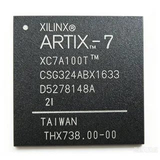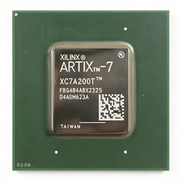
XC7A200T-2FBG484I - Artix-7 FPGA 215K Logic Cells | AMD Xilinx
MPN: XC7A200T-2FBG484I ✓ Active| Qty | Unit Price | Extended |
|---|---|---|
| 1 | $129.55 | $129.55 |
| 10 | $119.2 | $1,192.00 |
| 100 | $109.85 | $10,985.00 |
| 500 | $99.5 | $49,750.00 |
| 1,000 | $89.15 | $89,150.00 |
XC7A200T-2FBG484I Overview
An FPGA (Field-Programmable Gate Array) is a semiconductor device containing programmable logic blocks and interconnects that can be configured after manufacturing to implement custom digital circuits. FPGAs sit within the broader category of programmable logic devices (PLDs), which are part of the application-specific integrated circuit (ASIC) family, but offer reconfigurability that ASICs lack. The Artix-7 family is positioned as a mid-range FPGA optimized for cost-sensitive, high-volume applications requiring high-speed transceivers and DSP capabilities.
Key features include 740 DSP48E1 slices for high-throughput digital signal processing, 16 high-speed transceivers supporting up to 6.6 Gb/s, and 285 I/O pins with support for multiple I/O standards including LVCMOS, LVDS, and HSTL. The device also integrates a PCIe Gen2 block, 10/100/1000 Ethernet MACs, and an analog-to-digital converter (XADC) for system monitoring. The -2 speed grade provides balanced performance for logic and I/O, while the industrial temperature range ensures reliable operation in harsh environments.
Architecturally, the XC7A200T is built on the 28nm high-k metal gate (HKMG) process, offering a 50% lower power footprint compared to previous generations. The configurable logic blocks (CLBs) contain 6-input look-up tables (LUTs) and dual flip-flops, enabling efficient implementation of complex logic functions. The device supports partial reconfiguration, allowing dynamic updates to specific regions without disrupting the entire design.
Typical applications include software-defined radio (SDR), medical imaging, industrial motor control, and high-performance computing acceleration. The high transceiver count and DSP resources make it particularly suited for communications infrastructure, such as LTE/5G base stations and network switches, where high-speed serial links and parallel processing are essential.
When designing with this FPGA, careful attention must be paid to power supply decoupling and thermal management. The device requires multiple voltage rails (VCCINT, VCCAUX, VCCO) with proper sequencing, and the FBG484 package has a thermal resistance of 8.4°C/W (theta_JA) that necessitates adequate airflow or heatsinking for high-utilization designs.
Drop-in alternatives for XC7A200T-2FBG484I — same package, pin-to-pin compatible. Different-package parts requiring PCB rework are excluded.
Variants in this series
Same-series models that are drop-in compatible with XC7A200T-2FBG484I (same form factor and footprint) — differing in Package, Operating Temperature, Block RAM, Clock Management Tiles, DSP Slices.
Quick Comparison Tool — Select alternative parts for side-by-side comparison:
XC7A200T-2FBG484C
✅ Drop-In✓ In Stock
$320 / Unit
View Datasheet →XC7A200T-1FBG484I
✅ Drop-In✓ In Stock
$38.5 / Unit
View Datasheet →XC7A200T-3FBG484I
✅ Drop-In ⚠️ 参数待验证📋 Reference alternative (not in catalog)
XC7A200T-2FFG484I
✅ Drop-In ⚠️ 参数待验证📋 Reference alternative (not in catalog)
XC7A200T-2FBG484I Maximum Ratings & Electrical Characteristics
| Family | Artix-7 |
| Number of Logic Elements/Cells | 215360 |
| Number of LABs/CLBs | 16825 |
| Total RAM Bits | 13455360 |
| Number of I/O | 285 |
| Number of DSP Slices | 740 |
| Number of Transceivers | 16 |
| Transceiver Speed | 6.6 Gb/s |
| Supply Voltage | 0.95 V to 1.05 V (nominal 1 V) |
| Operating Temperature | -40°C to +100°C |
| Package | 484-BBGA, FCBGA (FBG484) |
| Mounting Type | Surface Mount |
| Speed Grade | -2 |
| RoHS Status | Compliant |
| Lead Free | Yes |
XC7A200T-2FBG484I Pin Configuration
| Pin A1 | GND — Ground |
| Pin A2 | VCCO_0 — I/O bank 0 supply voltage |
| Pin A3 | IO_L1P_T0_0 — I/O pin, bank 0 |
| Pin B1 | VCCINT — Internal core supply voltage (1V) |
| Pin B2 | IO_L1N_T0_0 — I/O pin, bank 0 |
| Pin C1 | VCCAUX — Auxiliary supply voltage |
| Pin C2 | IO_L2P_T0_0 — I/O pin, bank 0 |
| Pin D1 | GND — Ground |
| Pin D2 | IO_L2N_T0_0 — I/O pin, bank 0 |
| Pin E1 | VCCO_0 — I/O bank 0 supply voltage |
| Pin E2 | IO_L3P_T0_0 — I/O pin, bank 0 |
| Pin F1 | VCCINT — Internal core supply voltage (1V) |
Typical Applications
XC7A200T-2FBG484I is suitable for 6 applications: Software-Defined Radio (SDR), Medical Imaging, Industrial Motor Control, High-Performance Computing Acceleration, Communications Infrastructure, Test and Measurement.
Software-Defined Radio (SDR)
The XC7A200T-2FBG484I is ideal for SDR applications due to its 16 high-speed transceivers (up to 6.6 Gb/s) and 740 DSP slices. These resources enable efficient digital down/up conversion, filtering, and modulation/demodulation. The 13.4 Mb of Block RAM supports large buffers for wideband signals. The industrial temperature range ensures reliable operation in field-deployed radios.
Recommended
Medical Imaging
The XC7A200T-2FBG484I is well-suited for medical imaging systems like ultrasound and MRI, where high-speed data acquisition and processing are critical. Its 740 DSP slices handle beamforming and image reconstruction algorithms, while the 285 I/O pins interface with high-speed ADCs and DACs. The -2 speed grade provides the performance needed for real-time imaging.
Recommended
Industrial Motor Control
The XC7A200T-2FBG484I is ideal for industrial motor control applications, offering 740 DSP slices for implementing complex control algorithms like FOC (Field-Oriented Control). Its 285 I/O pins interface with encoders, current sensors, and gate drivers. The industrial temperature range (-40°C to +100°C) ensures reliable operation in harsh factory environments.
Recommended
High-Performance Computing Acceleration
The XC7A200T-2FBG484I can accelerate compute-intensive workloads in HPC systems. Its 740 DSP slices and 13.4 Mb of Block RAM enable efficient implementation of custom arithmetic units and data pipelines. The 16 transceivers provide high-bandwidth connectivity to host processors or other FPGAs, making it suitable for data center accelerators.
Recommended
Communications Infrastructure
The XC7A200T-2FBG484I is well-suited for communications infrastructure like LTE/5G base stations and network switches. Its 16 high-speed transceivers (up to 6.6 Gb/s) support CPRI, JESD204B, and 10GbE interfaces. The 740 DSP slices handle channel coding and equalization, while the 285 I/O pins interface with PHY devices and control planes.
Recommended
Test and Measurement
The XC7A200T-2FBG484I is ideal for test and measurement equipment like oscilloscopes and logic analyzers. Its 285 I/O pins interface with high-speed ADCs and DACs, while the 740 DSP slices handle triggering, decimation, and waveform processing. The 13.4 Mb of Block RAM supports deep acquisition buffers, and the -2 speed grade ensures high sample rates.
Recommended
Recommended Products Summary
Engineering reference data for XC7A200T-2FBG484I — comparison, design guidance, and compliance information.
Selection Guide
Comparison with Alternatives
| Parameter | This Product | XC7A200T-2FBG484C | XC7A200T-1FBG484I | XC7A200T-3FBG484I |
|---|---|---|---|---|
| Package | 484-BBGA, FCBGA (FBG484) | 484-BBGA, FCBGA (FBG484) - same | 484-BBGA, FCBGA (FBG484) - same | 484-BBGA, FCBGA (FBG484) - same |
| Brand | AMD | AMD | AMD | AMD |
| Logic Cells | 215360 | 215360 | 215360 | 215360 |
| Block RAM (bits) | 13455360 | 13455360 | 13455360 | 13455360 |
| Number of I/O | 285 | 285 | 285 | 285 |
| Speed Grade | -2 | -2 | -1 | -3 |
| Temperature Range | -40°C to +100°C | 0°C to +85°C | -40°C to +100°C | -40°C to +100°C |
| Supply Voltage | 0.95V to 1.05V | 0.95V to 1.05V | 0.95V to 1.05V | 0.95V to 1.05V |
Key Differentiators
- Industrial temperature range (vs XC7A200T-2FBG484C)
- Higher speed grade (vs XC7A200T-1FBG484I)
- Balanced performance and cost (vs XC7A200T-3FBG484I)
Design Notes
The XC7A200T-2FBG484I requires multiple voltage rails: VCCINT (1V), VCCAUX (1.8V), and VCCO (bank-specific). Proper power sequencing is critical to avoid latch-up or damage. Use a dedicated power management IC or FPGA power sequencer to ensure correct startup order. Decouple each rail with 100nF and 10uF capacitors placed close to the FPGA pins.
The FBG484 package has a thermal resistance of 8.4°C/W (theta_JA). For high-utilization designs, power dissipation can exceed 10W, requiring a heatsink or forced airflow. Calculate the junction temperature using Tj = Ta + (theta_JA * P) and ensure it stays below the maximum rated temperature of 100°C for industrial grade.
For the 484-ball FBGA package, use a 4-layer or more PCB with dedicated power and ground planes. Route high-speed transceiver signals with controlled impedance (e.g., 100 ohm differential for LVDS). Place decoupling capacitors as close to the FPGA as possible, and use via-in-pad for the thermal pad to improve heat dissipation.
Compliance Information
RoHS compliant and lead-free per Micro-Semiconductor.com. Not AEC-Q100 qualified as it is an FPGA, not an automotive-grade component.