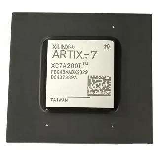
A3PE1500-1FGG484I - ProASIC3E FPGA 1.5M Gates | Microchip
MPN: A3PE1500-1FGG484I ✓ Active| Qty | Unit Price | Extended |
|---|---|---|
| 1 | $0 | $0.00 |
| 10 | $0 | $0.00 |
| 100 | $0 | $0.00 |
| 500 | $0 | $0.00 |
| 1,000 | $0 | $0.00 |
A3PE1500-1FGG484I Overview
An FPGA is a programmable logic integrated circuit that can be configured after manufacture to implement arbitrary digital logic. Unlike CPLDs, which are typically smaller and limited to combinational logic, FPGAs contain thousands of configurable logic blocks, embedded memory, and programmable I/O, allowing complex synchronous digital systems to be built without a custom ASIC. The ProASIC3E family sits in the FPGA product hierarchy as a non-volatile, flash-based FPGA, occupying a position between low-density CPLDs and high-density SRAM-based FPGAs. It is reprogrammable in the field yet retains its configuration when power is removed.
Key features include non-volatile flash configuration, which eliminates the need for external boot memory and provides live-at-power-up operation. The 1.5M system-gate density supplies adequate resources for soft processors, communication controllers, and video processing pipelines. The 280 user I/Os, arranged in multiple I/O banks, support a range of single-ended and differential signaling standards. The 276480 bits of SRAM provide true dual-port memory blocks for FIFOs and packet buffers. The -1 speed grade and 272 MHz performance give a strong balance of speed and power.
Technically, the device is fabricated on a 130 nm, seven-layer-metal (six copper) flash-based CMOS process. ProASIC3E FPGAs differ from SRAM-based FPGAs in that their configuration is stored in non-volatile flash cells, providing immunity to single-event upsets in configuration memory and simplifying secure IP retention. The flash fabric supports partial reconfiguration and on-chip programming through JTAG. The FPGA includes clock conditioning circuits (CCC) and phase-locked loops (PLLs) for robust clock generation; exact PLL count and I/O standard support should be confirmed from the datasheet Appendix.
Typical applications include wired and wireless communications line cards, industrial automation controllers, avionics data concentrators, medical imaging front-end processing, and ASIC replacement in mid-volume systems. In these roles, the A3PE1500-1FGG484I supplies deterministic, low-power logic with instant-on capability, reducing bill-of-materials cost and start-up complexity compared to SRAM FPGAs with external configuration devices.
A key design consideration is power integrity: the 1.5V core rail must be decoupled with a matrix of 100 nF and 10 uF ceramic capacitors placed near the FBGA balls, and the PCB should provide an unbroken ground plane beneath the package. Because the device is flash-based, configuration memory is non-volatile, but you still need to plan for JTAG programming header access during manufacturing and field updates.
This page synthesizes verified distributor data, drop-in alternative MPNs, and practical design guidance not found in the manufacturer datasheet, helping engineers evaluate A3PE1500-1FGG484I for new designs or replacement.
Drop-in alternatives for A3PE1500-1FGG484I — same package, pin-to-pin compatible. Different-package parts requiring PCB rework are excluded.
Variants in this series
Same-series models that are drop-in compatible with A3PE1500-1FGG484I (same form factor and footprint) — differing in Package, System Gates, Configuration Memory, Process Technology, Speed Grade.
Quick Comparison Tool — Select alternative parts for side-by-side comparison:
A3PE1500-FGG484I
✅ Drop-In📋 Reference alternative (not in catalog)
A3PE1500-2FGG484I
✅ Drop-In✓ In Stock
$195 / Unit
View Datasheet →A3PE1500-1FGG484
✅ Drop-In✓ In Stock
$48.1 / Unit
View Datasheet →A3PE1500-FG484I
✅ Drop-In📋 Reference alternative (not in catalog)
A3PE1500-1FG484I
✅ Drop-In📋 Reference alternative (not in catalog)
A3PE1500-2FG484
✅ Drop-In ⚠️ Specs Unverified✓ In Stock
$210 / Unit
View Datasheet →A3PE1500-1FGG484I Maximum Ratings & Electrical Characteristics
| Series | ProASIC3E |
| System Gates | 1.5M gates |
| Logic Elements | 16KLEs |
| Max System Performance | 272 MHz |
| Process Technology | 130nm, 7-layer metal (6 copper), Flash-based CMOS |
| Core Supply Voltage | 1.5V |
| Total RAM Bits | 276480 bits |
| User I/Os | 280 |
| Package Type | FBGA-484 |
| Ball Pitch | 1 mm |
| Pin Count | 484 |
| Mounting Type | Surface Mount |
| Speed Grade | -1 |
| Configuration Memory | Non-volatile Flash |
| Programming Interface | JTAG |
| Lifecycle Status | Active (listing available at major distributors) |
A3PE1500-1FGG484I fbga-484 Pin Configuration Guide
Pin configuration for A3PE1500-1FGG484I (fbga-484 package). This digital IC includes GPIO, communication interfaces (UART, SPI, I2C), and power pins. Refer to the manufacturer datasheet for alternate pin functions and configuration options. Essential for embedded system design and PCB layout.

No detailed pinout data available for A3PE1500-1FGG484I.
Refer to the datasheet for full pin configuration.
Typical Applications
A3PE1500-1FGG484I is suitable for 6 applications: Wired and Wireless Communications, Industrial Automation and Motor Control, Avionics and Defense, Medical Imaging and Monitoring, Consumer Electronics and Display Control, ASIC Replacement and System Integration.
Wired and Wireless Communications
The A3PE1500-1FGG484I is well suited for communications equipment such as line cards, Ethernet switches, and radio base stations because its 280 user I/Os and 276480 bits of true dual-port SRAM enable packet buffering, protocol controllers, and parallel bus interfaces. The flash-based configuration provides instant-on operation, which helps line cards begin forwarding traffic immediately after power-up. With 272 MHz system performance and -1 speed grade, the FPGA can handle high-speed data paths while maintaining deterministic timing. In these systems the device often sits between a host processor and PHY/MAC devices, performing framing, filtering, or interface translation. Microchip's ProASIC3E family is explicitly targeted at networking and communications applications, making this MPN a dependable choice for medium-density communications logic.
Recommended
Industrial Automation and Motor Control
In industrial automation, the A3PE1500-1FGG484I provides flexible glue logic for PLCs, motor drives, and robotic controllers. Its 1.5M system gates can implement multiple UART/SPI interfaces, quadrature encoder counters, PWM generators, and safety interlocks on a single chip. The non-volatile flash configuration means the FPGA can be live-at-power-up, simplifying field upgrades and avoiding the need for external configuration memory. The industrial temperature suffix (I) is critical for factory floor environments, though the exact temperature range should be confirmed in the datasheet. The 484-ball FBGA package offers enough I/Os to connect directly to MCU buses, gate drivers, and isolated interfaces. This reduces component count and board area in compact industrial controllers.
Recommended
Avionics and Defense
The A3PE1500-1FGG484I is attractive for avionics data concentrators, mission computers, and sensor interfaces because flash-based FPGAs retain configuration without external boot memory and are less susceptible to configuration single-event upsets. With 1.5M gates and 280 I/Os, the device can implement multiple communication standards, bus monitors, and data formatting logic in a single package. Microchip's ProASIC3E datasheet specifically mentions the avionics market as a target application. Designers should still perform radiation and qualification analysis for the specific program, and may consider military-grade M1 variants if extended temperature or screening is required. The -1 speed grade provides additional timing margin for high-integrity interfaces such as ARINC-429 or MIL-STD-1553 controllers.
Recommended
Medical Imaging and Monitoring
Medical imaging systems such as ultrasound and optical coherence tomography require parallel signal processing and sensor interface logic. The A3PE1500-1FGG484I provides 276480 bits of RAM for line buffers and image cache, while 280 I/Os connect to CMOS image sensors, ADCs, and display controllers. The 272 MHz system performance supports moderate image-processing pipelines such as filtering, contrast adjustment, and data packing. Flash-based instant-on capability is valuable for portable medical devices that must start quickly. The industrial temperature suffix is also relevant for compact medical instruments operating in warm environments. This device can replace multiple CPLDs or small ASICs, reducing design complexity and time-to-market for FDA-regulated equipment where change control is costly.
Recommended
Consumer Electronics and Display Control
For consumer display controllers and multimedia devices, the A3PE1500-1FGG484I can implement timing controllers, pattern generators, and interface translation between HDMI/LVDS and parallel RGB buses. The 280 I/Os allow multiple display interfaces to be connected directly, while the 276480 bits of RAM support small frame buffers and FIFOs. Flash configuration keeps the system cost low because no external configuration PROM is required, and field updates can be done through JTAG. The 1.5M gate density is sufficient for sub-systems such as scaling filter logic and remote-control codec blocks. With 272 MHz performance, the device can handle high-bandwidth video signals while leaving headroom for control logic. This makes it a flexible mid-density FPGA choice for next-generation consumer electronics.
Recommended
ASIC Replacement and System Integration
The A3PE1500-1FGG484I is an effective ASIC replacement for medium-volume products because it is reprogrammable and avoids non-recurring engineering costs. Its 1.5M gates and 280 I/Os allow consolidation of multiple legacy ASSPs, CPLDs, and logic chips into one device. The flash-based architecture ensures secure IP retention and instant-on behavior, reducing boot complexity in systems that previously required external configuration memory. The -1 speed grade provides the performance headroom to replicate existing synchronous interfaces. Engineers can prototype with the same FPGA that will be used in production, reducing risk and time-to-market. The 484-ball FBGA provides enough interconnect to route dense PCB designs without complex layer stack-ups.
Recommended
Recommended Products Summary
Engineering reference data for A3PE1500-1FGG484I — comparison, design guidance, and compliance information.
Selection Guide
Comparison with Alternatives
| Parameter | This Product | A3PE1500-FGG484I | A3PE1500-2FGG484I | A3PE1500-1FGG484 |
|---|---|---|---|---|
| Package | FBGA-484 (1 mm pitch) | FBGA-484 (1 mm pitch) | FBGA-484 (1 mm pitch) | FBGA-484 (1 mm pitch) |
| Brand | Microchip Technology | Microchip Technology | Microchip Technology | Microchip Technology |
| System Gates | 1.5M | 1.5M | 1.5M | 1.5M |
| Logic Elements | 16KLEs | 16KLEs | 16KLEs | 16KLEs |
| User I/Os | 280 | 280 | 280 | 280 |
| Total RAM Bits | 276480 | 276480 | 276480 | 276480 |
| Speed Grade | -1 | Standard | -2 | -1 |
| Temperature Grade | I suffix (industrial; confirm range in datasheet) | I suffix | I suffix | Commercial (no I) |
Key Differentiators
- -1 speed grade provides higher system performance (vs A3PE1500-FGG484I)
- Industrial temperature suffix for harsh environments (vs A3PE1500-1FGG484)
- RoHS-friendly FGG green package finish (vs A3PE1500-1FG484I)
Design Notes
Estimated: A high-utilization A3PE1500 design can draw several hundred mA from the 1.5V core rail. Place a 10uF bulk capacitor and multiple 100nF ceramic capacitors close to the core supply balls, and use a low-impedance 1.5V plane on an inner layer. A 1A-rated regulator is a reasonable starting point for the core plus I/O transients. According to Microchip ProASIC3E design guidance, no external configuration device is required, so the power-up sequence can be simpler than with SRAM FPGAs.
Estimated: For a design dissipating 2-3W in the FBGA-484 package, provide a thermal via array directly under the die and connect it to the system ground plane to improve heat spreading. Use at least a four-layer PCB with solid ground and power planes. Calculate junction temperature using the thermal resistance (theta_JA) from the datasheet; if the estimated junction temperature exceeds the industrial I suffix limit, add forced airflow or reduce I/O drive strength.
For production programming and field updates, route the JTAG pins TCK, TMS, TDI, and TDO to a standard 2x5 header. Add series resistors and ESD protection close to the connector. Because the FPGA is flash-based, configuration memory is non-volatile, but you still need to plan for in-system programming access and maintain a clean ground return for the JTAG signals.
With 280 user I/Os and 1 mm ball pitch, use controlled-impedance routing for high-speed signals. Set output slew rate and drive strength in Microchip Libero SoC software to reduce simultaneous switching noise. For differential pairs, keep trace lengths matched and maintain consistent pair spacing. Use dog-bone or via-in-pad fanout for the FBGA, and avoid routing high-speed traces directly beneath the FPGA unless a solid ground plane exists.
Compliance Information
Compliance data not provided in verified sources. The FGG package designator may indicate lead-free/RoHS-compliant finish, but this should be confirmed with Microchip documentation.