Produtos (32865)

ADF4113BRU - 4 GHz Integer-N RF PLL | Analog Devices
ADF4113BRU

ADF4113BRU - 4 GHz Integer-N RF PLL | Analog Devices

The Analog Devices ADF4113BRU is a single integer-N RF frequency synthesizer with a 4.0 GHz maximum operating frequency, programmable prescaler and charge pump, and a 16-pin TSSOP package. The device combines a low-noise digital phase-frequency detector, precision charge pump, programmable reference divider, programmable A and B counters, and a dual-modulus prescaler for local-oscillator generation in wireless receivers and transmitters. Its programmable architecture lets designers divide down a stable reference source and synthesize the required carrier frequency while controlling channel spacing through the reference divider, counters, and prescaler settings. An integer-N PLL is a frequency-synthesizer category in which the feedback prescaler and integer counters establish the output frequency while the phase-frequency detector and charge-pump network close the loop around a voltage-controlled oscillator. The ADF4110 family therefore belongs to the broader hierarchy of clock and timing ICs, frequency synthesizers, phase-locked loops, RF signal-chain ICs, and semiconductors. Integer-N operation simplifies control compared with fractional-N architectures, while the maximum RF input rate enables high-frequency local-oscillator designs when the VCO and loop bandwidth are suitable. The ADF4113BRU supports RF synthesis up to 4.0 GHz and includes programmable dual-modulus prescaling, programmable charge-pump currents, a separate charge-pump supply, and a programmable reference divider. The family documentation also identifies 3 V system operation. Separate charge-pump supply capability allows extended tuning-voltage headroom, which is useful when the external VCO requires a tuning range beyond the main supply rail. The programmable charge-pump current provides another control point for loop dynamics and reference-spur trade-offs. The internal signal path uses a low-noise digital phase-frequency detector, precision charge pump, programmable reference divider, A and B counters, and P/P+1 dual-modulus prescaler. This arrangement is intended for integer-N local oscillators in RF upconversion and downconversion paths. The 16-TSSOP body is 4.40 mm wide and corresponds to the 0.173-inch package description listed by DigiKey. Package, lead finish, and orderable suffix must be checked against the Analog Devices ordering guide before substituting an alternative. Typical uses include GSM and other wireless receiver or transmitter local oscillators, RF upconversion and downconversion blocks, communications test equipment, and frequency-generation subsystems. In such systems, the reference divider can reduce a high-frequency reference before comparison with the divided VCO output. The A counter, B counter, and dual-modulus prescaler determine the integer multiplication relationship, while the charge pump and external loop filter translate phase error into VCO tuning voltage. The principal design constraint is loop stability. Component values for the charge-pump, loop filter, and VCO must be derived for the actual reference frequency, target output frequency, prescaler, phase margin, and tuning range. RF routing also requires short, controlled-impedance paths, solid return planes, and careful separation between sensitive synthesizer inputs and high-energy clock or switching nodes. The ADF4113 datasheet family should be consulted for the complete pin table and application circuit. This product record combines verified manufacturer and distributor information with a focused comparison of same-package options, practical loop-filter and layout guidance, and commercial availability context. It is intended to help engineers confirm footprint, frequency capability, programming architecture, and source-document status before committing a PLL design to layout or production.

Cotação Contato
ADF4118BRU - 3 GHz Integer-N RF PLL | Analog Devices
ADF4118BRU

ADF4118BRU - 3 GHz Integer-N RF PLL | Analog Devices

The Analog Devices ADF4118BRU is a single-channel, integer-N RF phase-locked-loop frequency synthesizer rated to 3.0 GHz and packaged in a 16-pin TSSOP. It is designed for wireless receiver and transmitter local oscillators, where programmable division, frequency synthesis, and phase locking must be combined in one IC. According to the Analog Devices product page, the ADF4118 is currently marked production, and the listed starting price is $2.78 as of the verified distributor search on 2026-10-23. An RF PLL is a clock-and-timing integrated circuit that locks a voltage-controlled oscillator to a stable reference frequency. The ADF4118 family combines a low-noise digital phase-frequency detector, precision charge pump, programmable reference divider, programmable A and B counters, and a dual-modulus prescaler. This hierarchy places it under frequency synthesizers, clock and timing ICs, and semiconductor components used to control RF oscillators. The verified product classification identifies one RF PLL channel, integer-N synthesis, a maximum operating frequency of 3 GHz, and a 16-pin TSSOP package measuring 0.173 inch wide by 4.40 mm. Its programmable architecture supports local-oscillator generation in up-conversion and down-conversion sections of wireless receivers and transmitters. The precision charge-pump output drives an external loop filter, while the divided reference and counter paths establish the target synthesis ratio. The ADF4118 family architecture supports integer-N frequency synthesis by comparing the divided oscillator signal with a divided reference. Designers select divider and counter values, then calculate loop-filter components according to the Analog Devices family datasheet. This architecture is useful when a stable system reference is available and the required local-oscillator frequency must be generated with programmable division. It is not a general-purpose clock generator for applications where the output frequency is fixed and no feedback loop is required. Typical uses include wireless transmitter local oscillators, wireless receiver down-conversion, up-conversion mixers, and other RF signal chains that require synthesized frequencies. The 3 GHz capability is appropriate for RF systems whose local-oscillator requirements fall within the device range. Final suitability depends on reference frequency, prescaler settings, counter limits, loop-filter design, output buffering, and compliance with the manufacturer’s recommended operating conditions. For PCB implementation, keep the charge-pump trace and loop-filter components close to the device, maintain short RF paths, and use a controlled reference signal. The external loop filter is part of the frequency-control system; changing its resistance or capacitance can alter loop dynamics, phase margin, and spur performance. Designers should review the family datasheet and application guidance before fixing component values. This page combines the verified manufacturer classification, distributor package and pricing information, and cross-reference findings with practical selection guidance. It distinguishes confirmed data from specifications that require direct confirmation from the current Analog Devices datasheet, helping engineers identify the correct PLL family and package without confusing similar ADF4110 or ADF4154 devices.

Cotação Contato
ADF4159CCPZ - 13 GHz Fractional-N PLL Synthesizer | Analog Devices
ADF4159CCPZ

ADF4159CCPZ - 13 GHz Fractional-N PLL Synthesizer | Analog Devices

The Analog Devices ADF4159CCPZ is a 13 GHz fractional-N frequency synthesizer with modulation, fast and slow waveform generation, one CMOS output, and a 24-lead WFQFN exposed-pad package. It uses a 25-bit fixed modulus for subhertz frequency resolution, while its low-noise digital phase-frequency detector operates up to 110 MHz according to the manufacturer datasheet. The device accepts CMOS reference input and is intended for programmable clock, modulation, and waveform-generation systems. A frequency synthesizer is a clock-and-timing semiconductor that locks an output frequency to a stable reference. In the PLL hierarchy, the ADF4159 belongs to the fractional-N synthesizer and phase-locked-loop categories, combining a programmable reference divider, phase detector, charge pump, Sigma-Delta fractional interpolator, feedback dividers, and output drive circuitry. This allows a single device to generate a precisely controlled RF or clock output while retaining fine frequency adjustment. Key verified features include operation to 13 GHz, a 25-bit fixed modulus, direct modulation, fast-ramp waveform generation, and both fast and slow waveform generation. The listed supply conditions include AVDD and VP from 2.7 V to 3.45 V and DVDD and SDVDD at 1.8 V. These features make the synthesizer useful where an adjustable RF clock, modulation source, or test waveform is needed rather than a fixed-frequency oscillator. Technically, the PLL compares the divided feedback signal with the divided reference signal. Its digital PFD and charge pump drive the tuning path, while the Sigma-Delta fractional interpolator permits fine fractional frequency control. The verified data also identifies a 110 MHz PFD frequency. Values such as phase noise, lock time, reference input frequency range, output power, and temperature limits were not supplied and must be verified in the complete manufacturer datasheet before design release. Typical uses include RF and microwave signal generation, communications test equipment, clock modulation, laboratory waveform sources, and closed-loop systems requiring programmable frequency. In these applications, the 13 GHz ceiling provides broad tuning coverage, the fractional-N architecture provides fine resolution, and the waveform functions reduce the need for separate modulation circuitry. A key design consideration is loop-filter and reference implementation. The external loop filter, charge-pump settings, reference divider, feedback dividers, and output matching network must be designed together because they determine loop dynamics and spectral performance. RF routing also requires controlled impedance and careful separation of sensitive feedback and reference paths. This page combines verified manufacturer and distributor facts, a conservative drop-in assessment, package guidance, and engineering-focused comparison and design notes. It distinguishes documented values from missing data so engineers can review the part without relying on unverified specifications.

Cotação Contato
ADF4350BCPZ - Wideband Synthesizer w/ Integrated VCO | ADI
ADF4350BCPZ

ADF4350BCPZ - Wideband Synthesizer w/ Integrated VCO | ADI

The Analog Devices ADF4350BCPZ is a wideband frequency synthesizer with an integrated voltage controlled oscillator (VCO) that operates on a fundamental output frequency range of 2200 MHz to 4400 MHz. Housed in a 32-lead LFCSP (5 mm x 5 mm) exposed-pad package, the part enables fractional-N or integer-N phase-locked loop (PLL) implementations when paired with an external loop filter and an external reference frequency. Divide-by-1/2/4/8/16 output dividers extend usable RF outputs as low as 137.5 MHz. A PLL frequency synthesizer is a closed-loop feedback system that compares a divided VCO output to a reference oscillator and adjusts the VCO tuning voltage until the divided frequency phase-locks to the reference. Fractional-N division enables finer frequency resolution than integer-N at the cost of additional noise-shaping circuitry, while integer-N mode delivers the lowest in-band phase noise. ADF4350 supports both modes, letting engineers trade off resolution against phase-noise performance for applications ranging from cellular base stations to test instrumentation. Key features include an output frequency span of 137.5 MHz to 4400 MHz, a 3-wire SPI-compatible serial interface for register programming, an auxiliary RF output that can be muted independently, and a phase-frequency detector (PFD) that supports reference frequencies up to 200 MHz. The integrated VCO eliminates the need for a discrete resonator, simplifying BOM and reducing board area in radio designs. According to the Analog Devices datasheet, the part supports channel spacing down to a sub-1 Hz resolution when used in fractional-N mode with proper modulator settings. The architecture combines a high-resolution sigma-delta modulator, a low-noise charge-pump, and a wideband VCO that is prescaled for stable locking across process and temperature variations. The mute function is both pin- and software-controllable, allowing the part to be shut down during idle periods in time-division duplex systems to save power. Typical applications include cellular base-station transceivers (GSM, UMTS, LTE, 5G FR1), microwave point-to-point and point-to-multipoint links, satellite communications up-converters, wireless backhaul infrastructure, and bench-top RF signal generators. The 32-lead LFCSP package provides a compact thermal envelope suitable for dense multi-radio boards. When designing with the ADF4350BCPZ, route the charge-pump supply through a ferrite bead and bypass it with a 10 nF cap to minimize reference spurs, and place the loop-filter components as close to the CP and VT pins as practical. Avoid routing digital SPI lines adjacent to the RF outputs to prevent crosstalk into the synthesized spectrum. This page synthesizes distributor pricing, drop-in alternatives drawn from the Analog Devices family, and practical layout notes that complement - but do not replace - the manufacturer datasheet.

Cotação Contato
ADF4351BCPZ - 4.4 GHz Fractional-N PLL Synthesizer | Analog Devices
ADF4351BCPZ

ADF4351BCPZ - 4.4 GHz Fractional-N PLL Synthesizer | Analog Devices

The Analog Devices ADF4351BCPZ is a fractional-N or integer-N phase-locked-loop frequency synthesizer with an integrated voltage-controlled oscillator, a 2.2 GHz to 4.4 GHz fundamental VCO range, and operation up to 4.4 GHz. The device accepts a 10 MHz to 250 MHz reference input and is supplied in a 32-lead VFQFN exposed-pad package. It supports programmable integer and fractional frequency synthesis through an external reference and loop filter. An RF frequency synthesizer generates a stable, programmable output by locking a voltage-controlled oscillator to a reference through a phase-locked loop. The ADF4351 belongs to the PLL synthesizer and clock-generator hierarchy, integrating the synthesizer, VCO, programmable dividers, reference and feedback paths, and RF output circuitry. This integration reduces board-level design effort while retaining the flexibility required for external loop-filter optimization. According to the Analog Devices product page and datasheet, the ADF4351 supports fractional-N and integer-N synthesis, includes an integrated VCO, and is intended for wideband RF applications. The 10 MHz to 250 MHz input range and 2.2 GHz to 4.4 GHz fundamental VCO range make it suitable for microwave communication, wireless infrastructure, test equipment, radar-related RF signal chains, and frequency-agile RF systems. Its fractional-N operation permits fine frequency resolution when the reference and N-divider settings are selected appropriately. The device requires an external loop filter and external reference frequency. Filter component selection affects loop bandwidth, phase noise, reference-spur behavior, lock time, and the amount of ripple presented to the VCO control node. Designers should evaluate loop dynamics for each output frequency rather than assuming one filter network is optimal across the full 2.2 GHz to 4.4 GHz range. The exposed pad provides the required thermal and electrical connection to the PCB. Typical implementation places the ADF4351 between a stable reference source and an RF load or receiver/transmitter signal chain. The output can be filtered, buffered, or mixed according to the system requirement. Keep the reference and loop-filter connections short, provide clean supply decoupling, and use a controlled-impedance RF layout for the output path. Verify phase noise, spur levels, lock behavior, output power, and temperature performance with the final reference and filter implementation. For direct replacement, verify package dimensions, exposed-pad construction, pin assignments, register compatibility, reference range, VCO range, and supply limits. A similar frequency range alone is insufficient for drop-in use. This page combines verified manufacturer and distributor information with practical PLL design considerations, comparison fields, and sourcing-oriented FAQ answers. Pricing and availability should be confirmed with authorized distributors as of 2026-10-21.

Cotação Contato
ADG1204YCPZ-500RL7 - ±15V/+12V 4:1 iCMOS Multiplexer, 12-LFCSP
ADG1204YCPZ-500RL7

ADG1204YCPZ-500RL7 - ±15V/+12V 4:1 iCMOS Multiplexer, 12-LFCSP

The Analog Devices ADG1204YCPZ-500RL7 is a monolithic CMOS analog multiplexer comprising four single channels in a 4:1 (SP4T) configuration, built on Analog Devices' iCMOS (industrial CMOS) modular process that combines high-voltage CMOS with bipolar technologies. The device operates from a single analog supply of ±15 V or +12 V dual analog rails, with rail-to-rail signal handling and 3 V logic-compatible digital inputs, eliminating the need for a separate VL supply rail. Housed in a 12-lead LFCSP (3x3 mm) package with an exposed pad, it delivers an on-resistance of 190 Ω typical and ultra-low 1.5 pF off source capacitance. An analog multiplexer (mux) is a precision solid-state switch that routes one of multiple analog input channels to a common output under digital control. Within the broader signal-chain hierarchy, an analog mux sits between the analog front end (sensors, instrumentation amplifiers) and the data converter (ADC), occupying the same functional niche as a relay matrix but with orders-of-magnitude faster switching and no mechanical wear. Multiplexers like the ADG1204 trade raw RF bandwidth for very high DC accuracy and charge-injection performance, which is why they dominate precision data-acquisition and sample-and-hold front ends. Key features include <1 pC charge injection when switching channels (critical for glitch-free sample-and-hold), 33 V maximum supply range, fully specified rail-to-rail operation, fully specified ±15 V/+12 V performance, and 3 V logic-compatible inputs that interface directly to modern FPGAs and microcontrollers without level shifters. iCMOS construction ensures ultralow power dissipation in a footprint compatible with portable instrumentation. The exposed pad of the LFCSP-12 package provides a low-thermal-resistance path to PCB copper, supporting reliable operation across the -40 °C to +125 °C automotive/industrial temperature range. Architecturally, the ADG1204 uses four independent NMOS transmission gates with break-before-make switching and TTL/CMOS-compatible address logic. The sub-1 pC charge injection is achieved through a proprietary switch-driver topology that cancels the gate-drain overlap charge, making the device suitable for sample-and-hold applications where channel-to-channel switching transients would otherwise corrupt the held voltage. Typical applications include precision data acquisition front ends, sample-and-hold amplifiers, automated test equipment (ATE) channel selection, audio/video signal routing, and battery-powered instrumentation where the iCMOS low-power advantage matters most. The 3x3 mm LFCSP footprint also makes it a strong fit for space-constrained multi-channel designs. When designing with the ADG1204, observe that the on-resistance of 190 Ω is not constant across the signal range - it varies with VDS and is highest near the rails. For low-distortion audio applications, keep signal amplitudes within ±5 V of mid-supply where RON flatness is best. The exposed pad must be soldered to a sufficient ground plane to keep junction temperature within spec; thermal vias to internal ground layers are strongly recommended. This page synthesizes distributor pricing, drop-in alternatives, and practical design notes not found in the manufacturer datasheet alone.

Cotação Contato
ADG1204YCPZ-REEL7 - ±15V 4:1 iCMOS Mux, 190Ω, 12-LFCSP | ADI
ADG1204YCPZ-REEL7

ADG1204YCPZ-REEL7 - ±15V 4:1 iCMOS Mux, 190Ω, 12-LFCSP | ADI

The Analog Devices ADG1204YCPZ-REEL7 is a low-capacitance, low-charge-injection, monolithic CMOS analog multiplexer configured as a 4:1 single-pole four-throw (SP4T) switch, with an on-resistance of 190 Ω and packaged in a 12-lead LFCSP (3 mm × 3 mm). It operates from dual ±15 V supplies or a single +12 V supply, making it suitable for industrial analog signal chains where bipolar headroom is required. An analog multiplexer (MUX) is a semiconductor switch that routes one of multiple analog input signals to a common output line under digital logic control, and it sits within the broader category tree of analog switch -> multiplexer/demultiplexer -> interface IC -> integrated circuit. The ADG1204 uses ADI's iCMOS (industrial CMOS) process, which combines high-voltage CMOS and bipolar transistors on a single die to deliver ±15 V signal swings with the low power dissipation typical of CMOS logic. Key features include ultralow charge injection (typically < 1 pC), low on-capacitance for minimal signal distortion at high frequency, fast switching speed with a bandwidth suitable for video signals, and a break-before-make action that eliminates momentary shorting between adjacent channels. The digital interface accepts standard TTL/CMOS logic levels at the A0 and A1 address pins plus an active-low EN to put the device into a high-impedance state when disabled. Architecturally, the ADG1204 integrates four independent n-channel MOSFET pass gates whose sources connect to the common D pin and whose drains terminate at the four S1–S4 pins, with logic translation circuitry ensuring that 3 V microcontroller GPIO can reliably drive the part from ±15 V analog rails. The iCMOS process also enables latch-up immunity under over-voltage transients. Typical applications include data-acquisition front ends, sample-and-hold circuits, video signal routing, ATE (automatic test equipment) pin switching, and precision instrumentation multiplexers. The wide supply tolerance allows direct interfacing to ±12 V or ±15 V op-amp outputs in industrial control loops. When designing with this device, ensure logic levels at the address pins remain within 0 V to VDD regardless of analog signal swing, and place 0.1 µF decoupling capacitors as close as possible to each supply pin. The exposed pad on the LFCSP package must be soldered to the PCB ground plane to achieve the rated power dissipation and to maintain the specified on-resistance stability. This page synthesizes distributor pricing, drop-in pin-compatible alternatives, and practical PCB design notes not found in the standalone ADI datasheet.

Cotação Contato
ADG1206YCPZ-REEL7 - 16:1 iCMOS Mux, Low Cap, ±15V/12V | ADI
ADG1206YCPZ-REEL7

ADG1206YCPZ-REEL7 - 16:1 iCMOS Mux, Low Cap, ±15V/12V | ADI

The Analog Devices ADG1206YCPZ-REEL7 is a monolithic iCMOS analog multiplexer that switches one of sixteen inputs to a common output, controlled by 4-bit binary address lines A0, A1, A2, and A3, and is housed in a 32-lead LFCSP-WQ (5 mm × 5 mm) package with on-resistance of 200 Ω maximum. It is built on Analog Devices' iCMOS process technology, which combines high-voltage CMOS, bipolar, and DMOS elements to deliver ±15 V / +12 V dual supply operation with ultralow power dissipation and ESD protection. The part is supplied on a 7-inch reel (-REEL7) and is specified over the -40 °C to +125 °C extended industrial temperature range. A multiplexer (MUX) is a switching component that selects one of multiple analog input signals and forwards the chosen channel to a single output line, controlled by a digital address. MUX devices sit within the broader signal-chain hierarchy: analog switch → multiplexer → data-acquisition front-end → mixed-signal subsystem. The 16:1 configuration implemented in the ADG1206 is the single-ended counterpart to the differential 8:1 ADG1207, both built on the same iCMOS die family. Key specifications include 200 Ω on-resistance (max), 13 pF typical on-capacitance, 490 MHz -3 dB bandwidth, 75 ns tON / 85 ns tOFF transition times, and ±15 V or +12 V single-supply operation. Ultralow charge injection (typically <1 pC) and low parasitic capacitance make it well-suited for data-acquisition front-ends, sample-and-hold circuits, and precision instrumentation where minimal signal-glitch and fast settling are required. The LFCSP-WQ-32 package includes an exposed thermal pad that must be soldered to the PCB ground plane for proper thermal and electrical performance. The iCMOS architecture allows ±15 V analog signal swings while running from a low-voltage logic interface, eliminating the need for external level shifters. The latch-up-immune construction and ESD robustness exceed 4 kV HBM on the analog inputs, making the part tolerant of harsh industrial environments. Designers should note that the ADG1206YCPZ-REEL7 and the ADG1206YCPZ (tray) are the same die in different packaging media; the only difference is the carrier format (reel vs. tray) for high-volume assembly. Typical applications include automated test equipment (ATE) and switching matrices, data-acquisition systems, sample-and-hold amplifiers, medical imaging front-ends, communication system routing, and avionics signal multiplexing. The wide analog signal range and low distortion also suit audio routing and video switching designs. For battery-powered or precision portable instruments, the ultralow power dissipation (typically <0.5 µW quiescent) extends operating life. A key design consideration is the analog ground (AGND) and digital ground (DGND) pin arrangement: the LFCSP-WQ-32 package provides separate analog and digital ground pins that should be tied to a low-impedance ground plane to minimize crosstalk between the digital address lines and the analog signal path. Designers must also observe the absolute maximum analog input voltage of ±25 V with respect to AGND, even when the supplies are off, to avoid latch-up. This page synthesizes manufacturer datasheet parameters, distributor pricing as of 2026-10-06, drop-in cross-references, and practical design notes not consolidated in any single vendor listing, providing unique value beyond Digi-Key or Mouser product pages.

Cotação Contato
ADG1207YCPZ - Low Cap 8-Ch ±15V iCMOS Mux | Analog Devices
ADG1207YCPZ

ADG1207YCPZ - Low Cap 8-Ch ±15V iCMOS Mux | Analog Devices

The Analog Devices ADG1207YCPZ is a monolithic iCMOS analog multiplexer integrating eight differential channels in a 32-lead LFCSP-WQ (5x5 mm) package with 200 ohm on-resistance and ultra-low 1.5 pF off capacitance. It switches one of eight differential inputs to a common differential output, addressed by a 3-bit binary code on A0, A1, and A2, and operates from dual ±5 V to ±15 V supplies or a single 12 V supply with up to 33 V total range. An analog multiplexer (mux) is a semiconductor switch that routes one of multiple analog input signals to a single output line under digital control, forming the front-end of a data acquisition system. In the hierarchy of signal-chain components, the mux sits between sensors or transducers and downstream amplifiers or converters, and as a member of the analog switch IC family it is valued for low on-resistance, low capacitance, and fast settling. The ADG1207 belongs specifically to the iCMOS process family, which combines high-voltage CMOS with sub-micron logic to achieve low power and small footprint simultaneously. Key differentiating features include less than 1 pC charge injection over the entire signal range, rail-to-rail signal handling, break-before-make switching action that prevents momentary shorting between channels, and TTL/CMOS-compatible 3 V logic inputs that interface directly to modern microcontrollers and FPGAs. The wide 33 V supply range supports industrial ±15 V systems as well as single-supply 12 V designs, and the 200 ohm on-resistance remains flat across the signal range, minimizing distortion in precision paths. The device uses iCMOS construction, an Analog Devices process technology that places a high-voltage analog transistor layer on top of a sub-micron CMOS logic layer. This allows the analog switches to handle ±15 V signals while the address decoders operate at sub-5 V CMOS levels, achieving ultralow power dissipation and latch-up immunity in a compact surface-mount package. Typical applications include data acquisition front-ends, sample-and-hold circuits, automatic test equipment (ATE) signal routing, audio and video signal switching, battery-powered instrumentation, and avionics multiplexing. The differential 8:1 architecture is particularly suited for balanced signal chains such as professional audio, instrumentation amplifiers, and isolated ADC front-ends where common-mode rejection matters. When designing with the ADG1207YCPZ, ensure the address lines are stable before VDD ramps to avoid parasitic channel selection during power-up, and place 100 nF decoupling capacitors close to each supply pin. For highest DC accuracy in low-impedance loads, select the ADG1407 family instead, since the ADG1207's 200 ohm on-resistance dominates error in sub-kohm paths. This page synthesizes distributor pricing, verified drop-in alternatives, and practical design notes not found in the standalone datasheet, giving engineers a single source for selection, sourcing, and layout guidance.

Cotação Contato
ADG1208YRUZ-REEL7 - 8:1 iCMOS MUX, 16-TSSOP | Analog Devices
ADG1208YRUZ-REEL7

ADG1208YRUZ-REEL7 - 8:1 iCMOS MUX, 16-TSSOP | Analog Devices

The Analog Devices ADG1208YRUZ-REEL7 is a monolithic, single 8-to-1 analog multiplexer built on Analog Devices' iCMOS (industrial CMOS) process, packaged in a 16-pin TSSOP (YRU) with a 200 ohm on-resistance. It switches one of eight analog inputs to a common output as determined by 3-bit binary address lines A0, A1, and A2, operating from dual +/-5 V to +/-15 V supplies or a single +12 V supply across a 33 V supply range. An analog multiplexer is a semiconductor switch that routes one of multiple analog input signals to a single output line under digital control. MUXes belong to the broader category of analog switches and multiplexers, which sit under interface ICs and are essential building blocks in data acquisition (DAQ), instrumentation, audio routing, and automatic test equipment (ATE). The ADG1208's iCMOS process combines high-voltage CMOS with submicron CMOS, providing low power consumption, low on-resistance, and high switching speed in a small footprint. Key features include 200 ohm on-resistance (160 ohm per third-party sources), 5 ohm on-resistance flatness, +/-15 V dual supply operation, 1 pC charge injection, 2 pF off capacitance, 75 dB off-isolation, and 60 ns transition time. The device also offers break-before-make switching, rail-to-rail operation, 3 V logic-compatible digital inputs, and fully specified performance with +/-5 V, +5 V, +/-12 V, or +12 V supplies. The ADG1208 employs parallel CMOS switches with parasitic-junction-isolated bodies, enabling low charge injection and low capacitance. The wide supply range supports industrial signal levels up to +/-15 V while the 3 V logic interface allows direct connection to modern microcontrollers, FPGAs, and ADCs without level shifters. Typical applications include data acquisition front-ends, sample-and-hold systems, PLC analog input modules, ATE signal routing, audio/video signal switching, and battery-powered instrumentation. The TSSOP-16 footprint suits space-constrained PCB designs. When designing with the ADG1208, add 0.1 uF bypass capacitors near each supply pin and ensure unused digital address lines are tied to GND or VDD to avoid floating-state channel selection. The break-before-make architecture prevents momentary shorting between channels during switching transitions. This page synthesizes verified distributor pricing, pin-compatible drop-in alternatives, and application-specific design guidance not consolidated in the manufacturer datasheet, providing an engineering decision aid for sourcing and design-in.

Cotação Contato
ADG1213YRUZ - Quad SPST iCMOS Switch, 120Ω, ±15V | Analog Devices
ADG1213YRUZ

ADG1213YRUZ - Quad SPST iCMOS Switch, 120Ω, ±15V | Analog Devices

The Analog Devices ADG1213YRUZ is a monolithic iCMOS (industrial CMOS) quad SPST (Single-Pole Single-Throw) analog switch housed in a 16-pin TSSOP (YRU) package, featuring 1 pF off capacitance, 2.6 pF on capacitance, <1 pC charge injection, and 120 Ω on resistance. It operates from ±4.5 V to ±16.5 V dual supplies or up to +12 V single supply with rail-to-rail signal handling and 33 V maximum supply range. An iCMOS switch is a monolithic CMOS device that combines high-voltage CMOS and bipolar process steps, enabling analog switches that tolerate ±15 V supplies while still allowing 3 V logic-compatible control inputs without requiring a separate V_L rail. The ADG1211/ADG1212/ADG1213 family sits in the broader hierarchy of analog switches → multiplexers → signal-chain interface ICs → mixed-signal semiconductors, and serves as a precision, low-charge-injection building block between sensitive analog front ends and higher-voltage analog signal paths. Key differentiating features include four independently selectable normally-open SPST channels (the ADG1211 is normally-open, ADG1212 normally-closed, ADG1213 contains two of each - check device grade), sub-1 pC charge injection that minimizes transient switching disturbance on sample-and-hold capacitors, and typical power consumption below 0.03 µW, making it well suited for power-sensitive multi-channel instrumentation. The 120 Ω on resistance is fully specified at ±15 V and +12 V with a flat, low-distortion characteristic across the audio band. Architecturally, the ADG1213 leverages the iCMOS process to integrate high-voltage DMOS transistors alongside low-voltage CMOS logic on a single die, eliminating the need for a logic-level shifter supply and simplifying board-level power-tree design. Each switch is independently controlled by a TTL/CMOS-compatible digital input, and all four channels exhibit matched on-resistance and ton/toff timing for synchronized multi-channel sampling. Typical applications include precision data-acquisition front ends, audio and video signal routing, automated test equipment (ATE) multiplexers, medical instrumentation, communication systems, and battery-powered multi-channel sensor switching where charge injection and input capacitance directly affect measurement integrity. When designing with this device, place 0.1 µF or larger decoupling capacitors as close as possible to the VDD and VSS pins, and keep digital control traces isolated from analog signal paths to preserve the low charge-injection and low distortion performance. The TSSOP-16 footprint is compatible with ADG1211YRUZ and ADG1212YRUZ variants for design reuse across NC/NO options. This page synthesizes distributor pricing, drop-in alternatives, and practical design notes not found in the manufacturer datasheet, providing a single-source engineering reference for the ADG1213YRUZ.

Cotação Contato
ADG1219BRJZ-REEL7 - ±15V/12V iCMOS SPDT Switch SOT-23-8 | Analog Devices
ADG1219BRJZ-REEL7

ADG1219BRJZ-REEL7 - ±15V/12V iCMOS SPDT Switch SOT-23-8 | Analog Devices

The Analog Devices ADG1219BRJZ-REEL7 is a monolithic iCMOS SPDT (single-pole double-throw) analog switch housed in an 8-pin SOT-23 package, featuring an active-low EN input that simultaneously disables both channels. The device is fully specified at +12 V single supply and ±15 V dual supply rails, exhibits a low 200 ohm on resistance, less than 0.5 pC charge injection over the full signal range, and 2.5 pF off capacitance, making it well-suited for precision signal-chain switching in industrial and instrumentation systems. A SPDT (single-pole double-throw) analog switch is a fundamental building block of the analog switch and multiplexer family. It routes one input signal to one of two outputs, or vice versa, using MOSFET pass transistors controlled by a logic-level input. SPDT switches sit within the broader taxonomy of analog switches -> multiplexers -> interface ICs -> signal conditioning, where they are valued for their bidirectional signal paths, near-zero quiescent current, and ability to handle rail-to-rail analog signals. The iCMOS (industrial CMOS) process used in the ADG1219 allows high-voltage bipolar swings (±15 V / 12 V) on a monolithic CMOS die, combining low power consumption with the wide dynamic range traditionally reserved for junction-isolation processes. Key features that differentiate this part include break-before-make switching action that prevents momentary shorting between channels during transitions, a low 0.6 nA maximum off leakage current at 85 °C, and 3 V to 16.5 V single-supply operation without requiring a logic-level VL supply. The 2.5 pF off capacitance and sub-1 pC charge injection make the ADG1219 well matched to data-acquisition front ends where injected charge would otherwise corrupt sample-and-hold settling. Typical application circuits include audio signal routing, ATE (automatic test equipment) channel selection, video switching, precision data-acquisition multiplexers, and battery-powered instrumentation. The enable pin simplifies power-down sequencing in multi-channel systems, allowing designers to put unused switches into a high-impedance state with a single control line. When designing with this part, place 0.1 µF decoupling capacitors close to VDD and VSS pins to suppress logic-induced transients. Because the switch is bidirectional, source and drain terminals are interchangeable, simplifying PCB layout. For applications that exceed ±15 V signals, review the absolute maximum ratings in the manufacturer datasheet. This page synthesizes distributor pricing, drop-in alternatives, and practical design notes not found in the manufacturer datasheet alone.

Cotação Contato
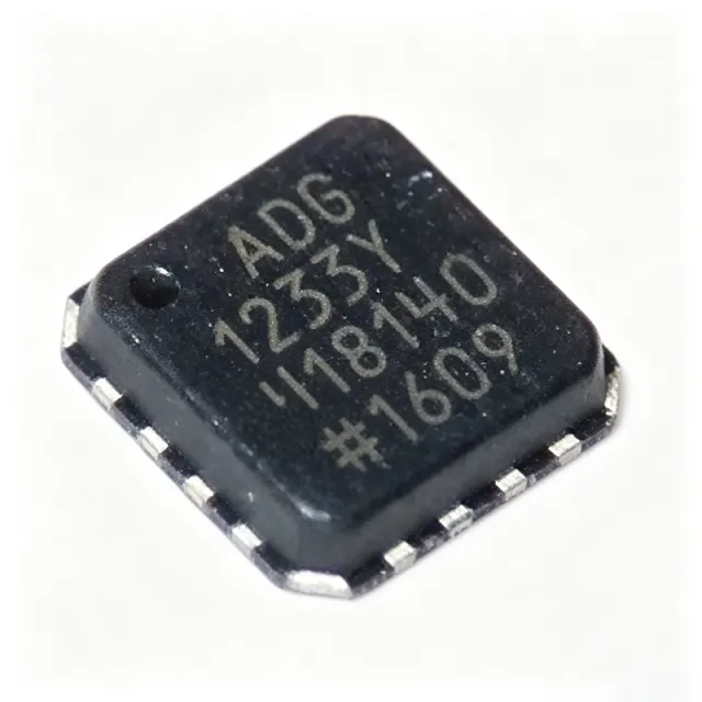
ADG1233YCPZ-REEL7 - Triple SPDT Analog Switch | Analog Devices
ADG1233YCPZ-REEL7

ADG1233YCPZ-REEL7 - Triple SPDT Analog Switch | Analog Devices

The ADG1233YCPZ-REEL7 is a monolithic iCMOS® analog switch from Analog Devices, integrating three independently selectable single-pole, double-throw (SPDT) switches in a compact 16-lead LFCSP-VQ (4x4 mm) package. It operates over a wide supply range of ±15 V or +12 V, with a low on-resistance of 120 Ω (typical) and ultra-low capacitance of 1.5 pF off capacitance, making it ideal for high-performance signal routing in precision instrumentation, audio, and data acquisition systems. An analog switch is a semiconductor device that selectively connects or disconnects an analog signal path under digital control. It is a fundamental building block in signal routing, multiplexing, and sample-and-hold circuits. The ADG1233 belongs to the family of analog switches and multiplexers, which are part of the broader category of interface ICs and signal conditioning components. Its iCMOS® (industrial CMOS) process technology ensures low power consumption and high voltage handling, bridging the gap between traditional CMOS and higher-voltage bipolar processes. Key features include break-before-make switching action, which prevents momentary shorting when switching channels, and an EN input that enables or disables the entire device. The switch is fully specified with 3 V logic-compatible inputs, allowing direct interface with low-voltage digital controllers. Rail-to-rail operation ensures minimal signal distortion across the full supply range. The 1.5 pF off capacitance and 0.5 pC charge injection minimize signal degradation in high-frequency and precision applications. The ADG1233 utilizes a proprietary iCMOS® process that combines the advantages of high-voltage CMOS with low power dissipation. This architecture enables the device to handle ±15 V supplies while maintaining low leakage currents and fast switching speeds. The break-before-make action is implemented through internal timing circuitry, ensuring reliable channel isolation during transitions. The device is available in a 16-lead LFCSP-VQ package, which offers excellent thermal performance and a small footprint for space-constrained designs. Typical applications include audio signal routing, precision data acquisition systems, automatic test equipment (ATE), and medical instrumentation. The low capacitance and charge injection make it particularly suitable for high-speed analog signals, while the wide supply range accommodates both bipolar and single-supply designs. The EN pin provides a convenient means of power-down or signal isolation in multi-channel systems. When designing with the ADG1233, ensure that the digital control signals are within the specified logic thresholds and that the supply voltages are properly decoupled with 0.1 µF capacitors close to the VDD and VSS pins. The break-before-make feature eliminates the need for external timing circuits, but the user should verify that the switching time meets system requirements.

Cotação Contato
ADG1236YCPZ-500RL7 - Dual SPDT ±15V iCMOS Analog Switch | ADI
ADG1236YCPZ-500RL7

ADG1236YCPZ-500RL7 - Dual SPDT ±15V iCMOS Analog Switch | ADI

The Analog Devices ADG1236YCPZ-500RL7 is a low-capacitance, low-charge-injection dual SPDT (single-pole double-throw) analog switch fabricated on the iCMOS process, offering a 33 V supply range, 1 pC charge injection, and 1.3 pF off capacitance in a 12-lead LFCSP (3 mm x 3 mm) package. An analog switch is an electronic component that routes or blocks analog signal paths under digital control. Within the signal-chain hierarchy, it belongs to the multiplexer/switch family of interface ICs, sitting between sensors or signal sources and amplifiers, ADCs, or measurement front ends. SPDT switches route one common terminal to one of two throw terminals, enabling source selection, gain-range switching, and redundant-path switchover in precision systems. Key features include 1.3 pF off capacitance and 3.5 pF on capacitance, which minimize signal distortion in high-frequency and capacitive-sensitive nodes, and 1 pC charge injection that reduces glitches when switching precision sample-and-hold or integrator circuits. The 33 V supply range supports +/-15 V dual-supply and 12 V single-supply operation, and the iCMOS process combines high-voltage CMOS and bipolar technologies for industrial-grade robustness. Logic inputs are 3 V logic-compatible and no VL supply pin is required, simplifying interfacing with low-voltage controllers. Technically, the iCMOS process allows high-voltage analog handling with low-voltage digital control, so the switch blocks up to +/-15 V signals while the control logic accepts standard 3.3 V or 5 V levels. The monolithic CMOS construction ensures low power and matched switch behavior across both SPDT channels, which switch independently for flexible routing. Typical applications include automated test equipment (ATE) signal routing, data-acquisition channel selection, precision sample-and-hold circuits, and industrial instrumentation where large-swing signals meet low-glitch switching requirements. Design consideration: on resistance is approximately 120 ohm typical (190 ohm maximum per DigiKey listing), so account for Ron flatness and voltage drop in high-impedance or precision-gain paths. This page synthesizes distributor pricing, drop-in alternative analysis, and practical design notes not found in the manufacturer datasheet, with data verified as of 2026-09-10.

Cotação Contato
ADG1408YRUZ - 8:1 CMOS Analog Multiplexer | Analog Devices
ADG1408YRUZ

ADG1408YRUZ - 8:1 CMOS Analog Multiplexer | Analog Devices

The Analog Devices ADG1408YRUZ is an 8:1 CMOS analog multiplexer with a maximum on-resistance of 4.7 ohms at 25°C, continuous current up to 190 mA, and 3 V-compatible logic inputs in a 16-lead TSSOP package. It switches one of eight inputs to a common output according to three binary address lines, A0, A1, and A2. An analog multiplexer is an analog switch network that connects one selected source channel to a shared destination. In the ADG1408, eight single-ended inputs are multiplexed onto one output. The address inputs control the selected path, while the common output provides a compact way to route signals in test equipment, data-acquisition systems, relay-replacement circuits, and audio/video equipment. This places the device in the interface IC hierarchy: analog switch → multiplexer → signal-routing IC. Key features include a maximum on-resistance of 4.7 ohms, on-resistance flatness of 0.5 ohm, rail-to-rail operation, and break-before-make switching. The manufacturer lists operation across ±15 V, +12 V, and ±5 V supplies, plus compatibility with 3 V logic inputs. These features make the ADG1408 suitable for systems that require controlled switching of bipolar or low-voltage signals while maintaining defined break-before-make behavior. The ADG1408YRUZ is specified in a 16-lead TSSOP package. Its 4.7-ohm maximum on resistance and 190-mA continuous-current capability provide useful performance for precision signal routing, although insertion loss and settling behavior depend on the source impedance, load, signal frequency, supply voltage, and layout. The 0.5-ohm on-resistance flatness helps minimize resistance variation across the selected switch network. Typical applications include relay replacement, audio and video routing, automatic test equipment, data-acquisition systems, and signal-path multiplexing. The break-before-make action is particularly useful where briefly connecting two externally driven sources is undesirable. For high-speed or high-impedance systems, engineers should evaluate switch capacitance, off leakage, charge injection, and clock timing in the complete signal path. The principal design consideration is ensuring that address transitions do not create an undesirable transient at the common output. Use the manufacturer-recommended supply bypassing, keep routing short, and account for the TSSOP footprint and pin orientation. This page combines the verified manufacturer and distributor information with engineering-oriented application guidance and sourcing details.

Cotação Contato
ADG1408YRUZ-REEL7 - 8:1 iCMOS Mux, 4.7Ω Ron, 16-TSSOP | ADI
ADG1408YRUZ-REEL7

ADG1408YRUZ-REEL7 - 8:1 iCMOS Mux, 4.7Ω Ron, 16-TSSOP | ADI

The Analog Devices ADG1408YRUZ-REEL7 is a monolithic iCMOS analog multiplexer that switches one of eight inputs to a common output, controlled by a 3-bit binary address (A0, A1, A2), housed in a 16-pin TSSOP (Y) package supplied on a 7-inch reel. It provides a typical on resistance (Ron) of 4.7Ω and a maximum Ron of approximately 5Ω across the specified signal range. An analog multiplexer (mux) is an analog switch array that time-multiplexes multiple analog input signals onto a single output line, allowing a microcontroller or ADC to sequentially sample many channels using only one ADC input. In the broader hierarchy, the ADG1408 belongs to the analog switch family, itself a subset of signal routing and interface ICs. The iCMOS (industrial CMOS) process used by Analog Devices combines high-voltage bipolar, CMOS, and DMOS transistors on a single die, enabling ±15 V / +12 V / ±5 V dual-supply operation while keeping leakage and Ron low. Key differentiating specifications include a 4.7Ω typical on-resistance, ±15 V dual-supply tolerance, low power consumption, latch-up proof construction, and break-before-make switching that prevents momentary shorting of input channels during channel transitions. The 3-bit binary address logic allows a simple GPIO or decoder to drive selection. The iCMOS architecture delivers high voltage tolerance with low Ron and low charge injection, making the ADG1408 suitable for industrial process control, instrumentation, and audio routing. Unlike low-voltage CMOS muxes (e.g., 4051-family parts limited to ~5 V), the iCMOS process lets designers route ±10 V or ±15 V signals directly without external level shifting. Typical applications include industrial process control PLCs, multi-channel data acquisition (DAQ) front-ends, audio/video signal routing, ATE (automatic test equipment) pin switching, and medical monitoring multiplexers. It is commonly paired with 16/18-bit ADCs to expand channel count. A key design consideration is supply sequencing: while iCMOS parts tolerate standard supplies, designers should add 100 nF decoupling close to VDD/VSS and consider ESD protection on field-side inputs. Break-before-make behavior eliminates cross-couples but limits simultaneous-channel sampling, so for simultaneous sampling use a per-channel amplifier + SAR front-end instead. This page synthesizes distributor pricing, drop-in alternatives in the same 16-TSSOP footprint, and practical design notes not found in the manufacturer datasheet alone.

Cotação Contato
ADG1411YCPZ-REEL7 - Quad SPST 1.8Ω Switch iCMOS | ADI
ADG1411YCPZ-REEL7

ADG1411YCPZ-REEL7 - Quad SPST 1.8Ω Switch iCMOS | ADI

The Analog Devices ADG1411YCPZ-REEL7 is a monolithic CMOS device containing four independently selectable single-pole single-throw (SPST) switches fabricated on ADI's iCMOS (industrial CMOS) process. The device features 1.8 Ω typical on-resistance, ±4.5 V to ±16.5 V dual-supply operation (or up to 12 V single-supply), 1.5 Ω on-resistance flatness, and is housed in a 16-lead LFCSP-VQ (4x4 mm) package. The four switches are normally-open (NO) types, sharing a common logic supply pin that interfaces directly to TTL and CMOS logic levels. An analog switch IC is a solid-state semiconductor device that uses MOSFET transistors to route analog signals between input and output terminals under digital control. SPST (single-pole single-throw) switches form the foundational building block of signal routing hierarchies: SPST -> SPDT -> multiplexer -> switch matrix -> signal chain. Analog switches sit at the boundary between the analog signal domain (where high linearity, low distortion, and low leakage are required) and the digital control domain (where logic-level compatibility is mandatory), making them essential in test equipment, instrumentation, data acquisition, and communication systems. Key specifications include a 1.8 Ω on-resistance (RON), 0.5 Ω channel-to-channel matching, 5 pC charge injection per switch transition, a -3 dB bandwidth of 115 MHz, and a turn-off isolation/break-before-make timing of 30 ns typical. The device operates from -40 °C to +125 °C extended industrial temperature range, drawing a quiescent supply current of typically 1 nA. The LFCSP-VQ-16 package integrates an exposed thermal pad that drops the junction-to-ambient thermal resistance to 33 °C/W on a standard JEDEC 4-layer board. The iCMOS architecture combines high-voltage CMOS transistors with submicron lateral bipolar structures on the same die, enabling analog signals up to ±16.5 V in a footprint that would otherwise require a larger 28 V bipolar process. This allows the ADG1411 to directly handle industrial-level signals without external level shifting, while still presenting logic inputs that are 1.8 V CMOS- and TTL-compatible. The break-before-make switching architecture prevents momentary shorting of signal sources during transitions. Typical applications include automated test equipment (ATE) pin electronics, precision data acquisition front-ends, audio/video signal routing, medical instrumentation multiplexing, industrial process control input switching, communication system gain-stage switching, and battery-powered portable instrumentation where the nanoampere quiescent current extends battery life. When designing with this part, place the exposed pad (pin 0) on a continuous copper ground plane with at least 16 thermal vias for heat extraction; bypass both VDD and VSS with 0.1 μF ceramic capacitors placed within 50 mm of the supply leads to control digital switching transients. Unused logic inputs must be tied to GND or VDD - never left floating - to prevent spurious channel activation. This page synthesizes distributor pricing from DigiKey, Mouser and Arrow, parameter-accurate drop-in alternatives, and practical PCB layout notes not found in the manufacturer datasheet.

Cotação Contato
ADG1434YRUZ-REEL7 - Quad SPDT 4.7Ω iCMOS Switch | ADI
ADG1434YRUZ-REEL7

ADG1434YRUZ-REEL7 - Quad SPDT 4.7Ω iCMOS Switch | ADI

The Analog Devices ADG1434YRUZ-REEL7 is a monolithic industrial CMOS (iCMOS®) analog switch integrating four independently selectable single-pole, double-throw (SPDT) channels in a 20-pin TSSOP package. Each channel exhibits a maximum 4.7 Ω on-resistance, 0.5 Ω on-resistance flatness, and rail-to-rail signal handling, all specified for ±15 V, +12 V, and ±5 V dual or single-supply operation. The 33 V supply maximum rating provides substantial transient headroom for industrial bus and instrumentation signal chains. An analog switch, sometimes called a CMOS switch or a bilateral switch, is a solid-state device that uses MOSFET transistors to pass or block analog signals with near-zero quiescent current. Analog switches sit hierarchically below multiplexers (MUX), which combine multiple switches with channel-selection logic, and belong to the broader Interface IC family that bridges real-world analog signals and digital control. Within this taxonomy, the ADG1434 specifically occupies the multi-channel SPDT niche — useful for signal routing, gain switching, sample-and-hold multiplexing, and audio/video signal steering where four channels are required. Key features include break-before-make switching action that prevents momentary shorting when channels change state, fully specified 3 V logic-compatible digital inputs for direct microcontroller interface without level shifters, and a TTL/CMOS-compatible enable input (active low) on selected package variants. The part achieves low power consumption suitable for battery-influenced portable systems while tolerating the bipolar supply rails demanded by precision analog front ends. The integrated iCMOS process enables the combination of high voltage tolerance, low on-resistance, and small TSSOP footprint that discrete relay or opto-isolated solutions cannot match. Typical applications include precision data-acquisition front ends, industrial process-control multiplexers, PLC analog input modules, instrumentation signal switching, medical monitoring routing, automated test equipment (ATE) channel selection, and audio/video signal routing in broadcast or studio equipment. The 4.7 Ω typical on-resistance and low charge injection make it suitable for 16-bit and lower-precision systems where signal-fidelity errors from RON contribute minimally to overall measurement uncertainty. When designing with this part, ensure logic inputs are driven with clean CMOS levels and that the analog signal range stays within both supply rails plus a small margin. Use adequate PCB ground copper and bypass the supply pins with 100 nF ceramic capacitors placed close to the package. The TSSOP-20 footprint is shared across the ADG1433 (3-channel), ADG1434 (4-channel), and ADG1436/ADG1439 families, enabling layout reuse across design variants. This page synthesizes distributor pricing, drop-in alternatives, and practical design notes not found in the manufacturer datasheet alone.

Cotação Contato
ADG1611BCPZ-REEL7 - 1Ω Quad SPST Switch | Analog Devices
ADG1611BCPZ-REEL7

ADG1611BCPZ-REEL7 - 1Ω Quad SPST Switch | Analog Devices

The Analog Devices ADG1611BCPZ-REEL7 is a quad single-pole single-throw (SPST) CMOS analog switch with 1 Ω typical on-resistance, housed in a 16-lead LFCSP-VQ (4 mm × 4 mm) package. The part contains four independent SPST switches that turn on with Logic 0 on the appropriate control input, conduct equally well in both directions, and accept input signal ranges that extend to the supplies. The -REEL7 suffix indicates a 7-inch (1500-piece) tape-and-reel packaging option. An analog switch (also called a CMOS switch or analog multiplexer switch) is a solid-state device that uses MOSFET transistors to route analog or digital signals between input and output pins under digital control. The ADG1611 sits within the broader hierarchy: analog switch → multiplexer/switch IC → interface IC → signal conditioning → data acquisition. Compared with electromechanical relays, CMOS analog switches offer vastly faster switching speeds, lower power consumption, no mechanical wear, and much smaller PCB footprint, at the cost of finite on-resistance and a limited signal-bandwidth product. Key features include 1 Ω typical on-resistance, 0.2 Ω on-resistance flatness across the signal range, ±3.3 V to ±8 V dual-supply operation, and 3.3 V to 16 V single-supply operation. The device does not require a V_L logic supply, accepts 3 V logic-compatible inputs directly, and supports rail-to-rail operation. Continuous current per channel is rated at 280 mA in the LFCSP package and 175 mA in the TSSOP variant. The ADG1611 is built on Analog Devices' iCMOS (industrial CMOS) process technology, which combines high-voltage analog capability with sub-µm CMOS digital logic on a single die. Typical applications include precision signal routing in data-acquisition front-ends, video and audio signal switching, ATE (automated test equipment) channel selection, instrumentation gain-stage multiplexing, communications systems, and battery-powered portable designs that benefit from the wide single-supply range. The wide supply tolerance also makes the device suitable for ±5 V industrial analog rails. When designing with the ADG1611, keep in mind that on-resistance varies with the input signal level (typical flatness is 0.2 Ω), so the part is not ideal for applications requiring gain-invariant signal chains without compensation. Add 0.1 µF decoupling capacitors close to VDD and VSS pins, and ensure unused logic inputs are tied to a valid logic level to prevent unwanted channel activation. This page synthesizes verified distributor pricing, drop-in alternative MPNs, parametric comparison tables, and practical design notes not found in the manufacturer datasheet alone.

Cotação Contato
ADG2188BCPZ - 8x8 Analog Crosspoint Switch | Analog Devices
ADG2188BCPZ

ADG2188BCPZ - 8x8 Analog Crosspoint Switch | Analog Devices

The ADG2188BCPZ is an 8x8 analog crosspoint switch from Analog Devices, designed for routing analog signals in telecommunications, ultrasound, and audio applications. It features 64 bidirectional switch channels arranged in an 8x8 array, with each switch individually addressable via an I2C-compatible interface. The device operates from a single 3.3V or 5V supply and is available in a 32-lead LFCSP-VQ (5x5 mm) package. An analog crosspoint switch is a matrix of switches that connects any input to any output, enabling flexible signal routing without external wiring. It is a key building block in signal routing systems, allowing multiple signals to be directed to different destinations under software control. The ADG2188 belongs to the family of analog switches and multiplexers, which are essential in applications requiring signal distribution and switching. Key features include low on-resistance, low leakage currents, and high bandwidth, ensuring minimal signal distortion. The I2C interface supports standard, full, and fast modes, allowing easy integration with microcontrollers. The device also includes an address pin for multiple device configuration on the same bus, and a reset pin for initialization. Technically, the ADG2188 uses CMOS technology to achieve low power consumption and high switching speed. The switch array is bidirectional, meaning rows and columns can be configured as inputs or outputs, providing flexibility in signal routing. The device also features break-before-make switching to prevent momentary short circuits during channel changes. Typical applications include telecommunications switching, ultrasound imaging, audio routing, and automatic test equipment. In telecommunications, it can route multiple channels in a central office; in ultrasound, it can switch transducer elements; in audio, it can route signals in mixing consoles. When designing with the ADG2188, ensure proper decoupling of the power supply and careful layout to minimize crosstalk. The I2C address pins should be set correctly to avoid bus conflicts. The device is RoHS compliant and suitable for surface-mount assembly.

Cotação Contato
ADG2188BCPZ-RL7 - 8x8 Analog Crosspoint Switch | Analog Devices
ADG2188BCPZ-RL7

ADG2188BCPZ-RL7 - 8x8 Analog Crosspoint Switch | Analog Devices

The ADG2188BCPZ-RL7 is an I2C CMOS 8x8 unbuffered analog switch array from Analog Devices, designed for routing analog signals in telecommunications, ultrasound, and audio applications. It provides 64 bidirectional switch channels arranged in eight columns by eight rows, with each switch individually addressable via a standard I2C-compatible interface. The device operates from dual or single supplies, supporting a wide analog signal range, and is housed in a compact 32-lead LFCSP-VQ (5x5 mm) package. An analog crosspoint switch is a type of analog switch array that allows any input to be connected to any output, enabling flexible signal routing without mechanical relays. It is a key building block in signal routing and switching systems, sitting between discrete analog switches and full digital crosspoint ICs in the signal chain hierarchy. The ADG2188's 8x8 matrix provides a balance of channel count and package size, making it suitable for dense PCB designs. Key features include a low on-resistance of [DATA_NEEDED: on-resistance] ohms, low leakage currents, and a wide operating voltage range. The I2C interface supports standard and full-speed modes, allowing easy integration with microcontrollers. The device also features a reset pin and address pins for multiple device configuration on the same bus. Its bidirectional architecture simplifies PCB layout by allowing rows and columns to be configured as inputs or outputs. Technically, the ADG2188 uses CMOS technology to achieve low power consumption and high signal integrity. The unbuffered architecture preserves signal fidelity, making it ideal for precision analog applications. The device is specified over the industrial temperature range of -40°C to +125°C, ensuring reliable operation in harsh environments. Typical applications include telecommunications switching, ultrasound imaging systems, audio routing, and automated test equipment. In ultrasound, the ADG2188 routes transducer signals to processing channels, while in audio, it enables flexible mixing and routing. Its low distortion and high bandwidth make it suitable for high-frequency signals. When designing with the ADG2188, ensure proper decoupling on the supply pins and consider the on-resistance flatness for precision applications. The I2C address pins allow up to [DATA_NEEDED: number of addressable devices] devices on a single bus, enabling large switch matrices.

Cotação Contato
ADG431BRZ-REEL7 - Quad SPST 24Ohm Analog Switch | Analog Devices
ADG431BRZ-REEL7

ADG431BRZ-REEL7 - Quad SPST 24Ohm Analog Switch | Analog Devices

The ADG431BRZ-REEL7 from Analog Devices is a monolithic CMOS analog switch IC containing four independently selectable SPST (single-pole single-throw) switches. Fabricated on the enhanced LC2MOS process, it combines low power dissipation with high switching speed and low on-resistance of 24 ohms maximum. Each switch conducts equally well in both directions when ON and turns on with a logic LOW on its control input. The device is supplied in a 16-pin SOIC package on tape and reel (REEL7) for automated surface-mount assembly. An analog switch IC is a semiconductor device that selectively connects or disconnects an analog signal path under digital control, replacing mechanical relays with faster, smaller, more reliable solid-state switching. Analog switches sit within the broader hierarchy of signal routing components: analog switch, multiplexer/demultiplexer, signal conditioning IC, and mixed-signal semiconductor. The ADG431 belongs to the ADG431/ADG432/ADG433 precision quad SPST family, which differs only in control-input logic polarity. Key features include the 24 ohm maximum on-resistance with low on-resistance flatness, glitch-free switching that suppresses charge-injection transients during state changes, bidirectional signal capability, and an operating temperature range of -40C to +85C for industrial environments. The LC2MOS process merges CMOS logic with linear Bipolar-grade analog capability, delivering fast transition times with microamp-level quiescent power consumption, ideal for battery-operated and high-density designs. Typical applications include audio and video signal routing, data acquisition channel selection, communication-system signal switching, and automated test equipment. Its low on-resistance minimizes insertion loss, while fast switching supports high channel-scan rates in multiplexed ADC front ends. When designing with this part, account for on-resistance-induced attenuation in series with source impedance, and observe supply-voltage limits. Note the active-LOW control logic: if your firmware assumes active-HIGH switching, the ADG432 is the logic-compatible family alternative in the identical SOIC-16 pinout.

Cotação Contato
ADG508FBNR - 8-Channel Fault-Protected Analog MUX | Analog Devices
ADG508FBNR

ADG508FBNR - 8-Channel Fault-Protected Analog MUX | Analog Devices

The Analog Devices ADG508FBNR is a CMOS 8-channel single-ended analog multiplexer with integrated fault protection, packaged in a 16-pin narrow-body SOIC (NB SOIC-16, R-16 Suffix) and rated for -40C to +85C industrial operation. It accepts dual supplies of +/-15 V typically (with +/-10.8 V to +/-16.5 V tolerance) or a single supply up to +15 V, and provides a low typical on-resistance of 300 ohm with fast tON/tOFF of 250 ns maximum each. A fault-protected analog multiplexer (MUX) is a specialized analog switch IC that tolerates overvoltage and power-loss events at its signal pins without damage to downstream circuitry or signal sources, distinguishing it from a standard CMOS analog MUX which has no such protection. The ADG508F family sits within the broader hierarchy of analog switches -> multiplexers (8:1, 4:1, dual 4:1) -> data acquisition components -> signal chain ICs used to expand a single ADC channel across many sensors or test points. Key features include true bidirectional operation, break-before-make switching, all switches off when supplies are removed, and analog output clamping that holds the ON channel within the supply rails during fault events. The series n-channel, p-channel, n-channel MOSFET structure provides both device-level and source-side overvoltage protection, making the part resistant to signals that exceed the supply range, even without external limiting resistors. Typical applications include industrial process control multiplexers, automated test equipment (ATE) signal routing, data acquisition front-ends, and any system where field-wired signals may encounter transients, miswiring faults, or hot-plug events. The fault-protection feature eliminates the need for external protection circuits in many designs. When designing with the ADG508FBNR, place a 0.1 uF decoupling capacitor close to the supply pins and ensure the address lines are driven with clean logic levels to avoid transient cross-talk. Avoid long input traces that couple noise into the high-impedance off-state channels. This page synthesizes real distributor pricing, drop-in alternatives, and design notes that supplement the manufacturer datasheet with engineer-focused selection guidance not available on stock pages.

Cotação Contato
ADG508FBRUZ - Fault-Protected 8:1 Analog MUX | Analog Devices | TSSOP-16
ADG508FBRUZ

ADG508FBRUZ - Fault-Protected 8:1 Analog MUX | Analog Devices | TSSOP-16

The Analog Devices ADG508FBRUZ is a CMOS 8:1 analog multiplexer with integrated overvoltage fault protection, presented in a 16-pin TSSOP (RU) package. It routes one of eight single-ended analog inputs to a common output, with a typical on-resistance of 270 ohm and typical on-resistance flatness of 8 ohm. The device operates from +/-15 V dual supplies or a single +12 V supply with supply range from +/-15 V up to +16.5 V (per digchip excerpt). A fault-protected analog multiplexer is a precision switching element that, unlike a standard analog mux, clamps its analog input and output within the supply rails when an overvoltage occurs on either an off-channel source or the main supply, and remains safe even if the supply is collapsed. The ADG508F belongs to the analog switch family (analog switch -> analog multiplexer -> data-acquisition component -> signal chain IC), and the ADG508F is the 8-channel single-ended variant, while the ADG509F is its 4-channel differential cousin. Key features include +/-30 V overvoltage protection on signal inputs independent of supply, latch-up-proof construction using series N-channel/P-channel/N-channel MOSFET structure, break-before-make switching action (tON ~225 ns, tOFF ~150 ns), low leakage of 10 nA maximum at 25 C, low charge injection, and ESD rating >2 kV HBM. The RU suffix denotes the 16-pin TSSOP package; the wider industrial temperature range of -40 C to +85 C makes the part suitable for harsh environments. The ADG508F uses a proprietary series-MOSFET architecture that limits current flow during a fault event and clamps voltages at the rails. This allows hot insertion of signals up to +/-30 V beyond the supply rails without damaging the IC, a level of robustness that standard muxes like the ADG508 or ADG1208 cannot provide. Typical applications include industrial data acquisition front-ends, process control PLC analog input modules, avionics and instrumentation signal routing, and battery cell monitoring where high common-mode transients are present. The fault-protection feature is particularly valuable in factory automation where wiring faults and ESD events are common. When designing with this device, ensure that VDD and VSS bypass capacitors are placed as close as possible to the supply pins. The address inputs (A0/A1/A2) are TTL/CMOS-compatible; a logic low on EN disables all channels and pulls the common to a high-impedance state. Avoid exceeding +/-30 V on any signal input, even during fault conditions.

Cotação Contato