Produtos (39.000+)

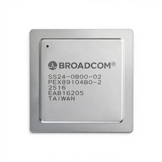
SS24-0B00-02 - 104-Lane PCIe 5.0 Switch | Broadcom PEX89000
SS24-0B00-02

SS24-0B00-02 - 104-Lane PCIe 5.0 Switch | Broadcom PEX89000

The Broadcom SS24-0B00-02 is a 104-lane PCI Express 5.0 switch based on the Broadcom / Avago PEX89104B0-2-DB device, designed as an integrated, multi-function PCI Interface IC for high-performance server, storage, and accelerator fabrics. It is sold as a specialized PCI Interface component and serves as the silicon core used in Broadcom PEX89000-series evaluation boards and OEM modules. The part operates as a fan-out switching element with internal non-transparent and transparent bridge capability, enabling multi-host and domain partitioning topologies required by modern disaggregated compute designs. A PCI Express switch is a hot-pluggable, packet-routing device that sits between a root complex and one or more endpoints (or additional switches), forwarding Transaction Layer packets according to PCIe routing rules. SS24-0B00-02 belongs to the hierarchical product family PCIe switch -> PCI bridge / switch -> PCI Express switch -> peripheral / interface IC, and ultimately to integrated circuits -> specialized / interface ICs. The PCIe 5.0 specification doubles the per-lane signaling rate to 32 GT/s compared with PCIe 4.0, doubling bandwidth to roughly 3.94 GB/s per direction per lane. By aggregating 104 lanes, the switch can deliver multi-terabit fabric throughput and is engineered to support the higher port counts demanded by NVMe-oF, CXL-attached memory pools, and heterogeneous AI/GPU compute racks. Key features of the SS24-0B00-02 include PCIe 5.0 compliance with backward support for PCIe 4.0/3.0 devices, a 104-lane configuration organized into multiple ports, advanced error reporting and AER support, hot-plug readiness, NVMe and CXL-aware QoS structures, and support for SR-IOV and multiple function hierarchies. The silicon also includes Enhanced Hot-Plug controllers, ECRC, Poisoned TLP handling, and Advanced Power Management (ASPM L0s/L1/L2) capabilities typical of the PEX89000 generation. Architecturally, the device integrates SerDes blocks capable of PCIe 5.0 long-reach signaling, a non-blocking internal switch fabric with credit-based flow control, and embedded MCUs for I2C/SMBus manageability. The silicon targets enterprise servers, NVMe SSD arrays, GPU/CPU accelerator backplanes, and composable infrastructure platforms, where it typically appears as a stand-up PCIe card or a BGA-mounted mezzanine. Typical applications include high-port-count NVMe-oF SSD backplanes, disaggregated CXL memory pools, AI training cluster fabric switches, hyperscale accelerator baseboards, and high-speed test & measurement PCIe capture cards. When integrating this part, designers must follow Broadcom's reference layout for the BGA-EP package, manage the multi-rail power-up sequence, and provide sufficient airflow to dissipate the high SerDes power at PCIe 5.0 data rates. Engineers typically source the SS24-0B00-02 from authorized distributors such as DigiKey, Mouser, and Avnet Americas for new designs; later-stage replacement is sometimes supported by Broadcom via the cross-reference SS26-0B00-02 (60V equivalent) for higher-voltage tolerance retrofit programs. This page synthesizes distributor pricing, drop-in alternatives, and practical design notes not found in the manufacturer datasheet.

USD $825,00 Em estoque
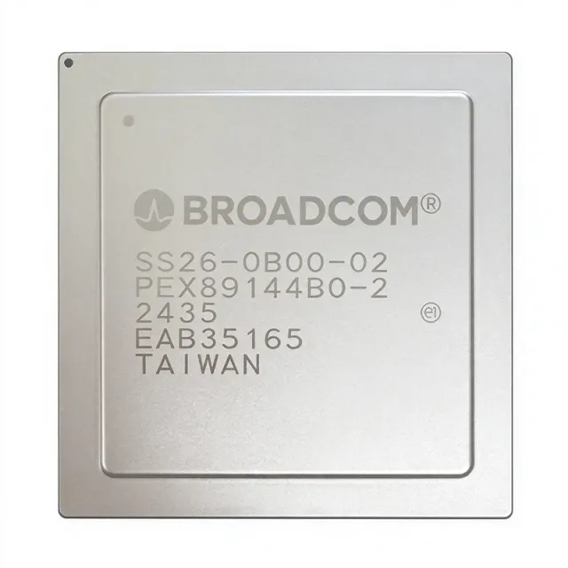
SS26-0B00-02 - PEX89144 PCIe Gen 5.0 Switch | Broadcom | 144-Lane
SS26-0B00-02

SS26-0B00-02 - PEX89144 PCIe Gen 5.0 Switch | Broadcom | 144-Lane

The Broadcom SS26-0B00-02 (associated die: PEX89144) is a 144-lane PCI Express 5.0 switch IC operating at 32 GT/s per lane, designed for high-end server, storage, and AI/ML fabric interconnects. As a member of the PEX89000 family of managed PCIe Gen 5.0 switches, it enables fan-out, partitioning, and non-transparent bridging across a heterogeneous set of root complexes and endpoints in modern accelerated-compute platforms. The part is supplied as a bare-die / specialized Broadcom package designated "SS26" and is targeted at OEM designs that integrate directly onto high-speed signal substrates. A PCIe switch is a protocol-aware layer-2 bridge device that replicates the PCI Express transaction layer and link layer across multiple ports, allowing one or more host processors to share a fabric of endpoints (NVMe SSDs, GPUs, NICs, accelerators) without requiring every device to live behind a single root complex. PCIe Gen 5.0 doubles the per-lane signaling rate to 32 GT/s versus Gen 4.0's 16 GT/s, doubling available bandwidth per lane to approximately 3.94 GB/s in each direction. Switches in this class sit within the broader taxonomy: PCIe switch -> PCIe interface IC -> peripheral controller -> integrated circuit -> semiconductor. Key features include 144 SerDes lanes arranged in 24 ports, support for hot-plug, surprise-down error reporting, Advanced Error Reporting (AER), SR-IOV with up to 256 physical functions per port, Multi-Root I/O virtualization (MR-IOV), and Broadcom's proprietary Adaptive Voltage Scaling / link-training diagnostics. The device integrates on-chip reference clocks, lane margining, and equalization controls required for Gen 5.0 signal integrity on long-reach backplane channels. Typical applications span hyperscale AI training fabrics where multiple GPUs share NVMe-oF storage, composable disaggregated servers, high-port-count NVMe SSD enclosures, and EBOF (Ethernet Bunch of Flash) reference platforms. The PEX89000 series extends Broadcom's PEX9700/8700/88000 lineage into Gen 5.0 territory, allowing customers to migrate existing Gen 3/4 designs with minimal firmware changes while doubling interconnect bandwidth. When designing with this device, follow Broadcom's PEX89000 hardware reference manual for PCB stackup, AC-coupling capacitor placement, and reference-clock routing. Always confirm lane assignment and bifurcation mode through the I2C/SMBus initial-provisioning interface before system bring-up.

USD $1.968,75 Em estoque
SSD1681 - 200x200 EPD Display Driver/Controller | Solomon Systech
SSD1681

SSD1681 - 200x200 EPD Display Driver/Controller | Solomon Systech

The Solomon Systech SSD1681 is an Active Matrix Electrophoretic Display (EPD) driver with integrated controller for Red/Black/White e-Paper panels. It delivers 200 source outputs, 200 gate outputs, 1 VCOM and 1 VBD channel, supporting a maximum display resolution of 200x200 pixels at single-chip level. An EPD (Electrophoretic Display) controller is a mixed-signal IC that drives the bistable pigment particles inside an e-Paper panel, generating visible text and graphics without backlight. The controller hierarchy flows: EPD driver -> display driver IC -> flat-panel controller -> mixed-signal semiconductor IC. Because e-Paper pixels are bistable, the SSD1681 only needs to refresh the panel when the displayed image changes, making it the workhorse driver for ultra-low-power electronic shelf labels (ESL), wearables, and IoT indicators. Key features include support for Mono Black/White and 3-color Red/Black/White panels, an embedded charge-pump booster for generating gate driver voltages, on-chip regulators and oscillator, and a hardware-selectable serial peripheral interface (SPI) for MCU command and image data transfer. The integrated DC-DC booster eliminates external high-voltage transistors and minimizes BOM area. Architecturally, the SSD1681 integrates a 200-bit source shift register, a 200-bit gate scan register, 1 VCOM driver, 1 border (VBD) driver, waveform look-up tables (LUTs) for grayscale and color transitions, and an OTP memory for default panel parameters. The internal temperature sensor and SPI command set allow the host to trigger optimal drive waveforms for the connected e-Paper panel. Typical applications include 1.54" and 2.13" e-Paper panels for electronic shelf labels, smart badges, logistics trackers, wearables, IoT sensor displays, and low-power information panels. The SSD1681 is widely adopted on Waveshare, Adafruit and BuyDisplay breakout boards. When designing with this IC, ensure that the host MCU supplies 3.3V logic to VCI/VDDIO and that the VPP/VNN charge-pump capacitors are sized per the panel's voltage sequence. The BUSY_n line must be polled before initiating SPI commands because e-Paper refresh cycles (typically 2 seconds for full update) are long compared to microsecond-scale SPI transactions. This page synthesizes distributor availability, drop-in alternatives, and practical design notes not found in the manufacturer datasheet, delivering unique engineering value beyond what distributor product listings provide.

Cotação Contato
SSD1963 - 1215KB Frame Buffer LCD Controller, 864x480 | Solomon Systech
SSD1963

SSD1963 - 1215KB Frame Buffer LCD Controller, 864x480 | Solomon Systech

The Solomon Systech SSD1963 is a display controller IC with 1215K byte embedded frame buffer supporting up to 864 x 480 x 24-bit graphics content, housed in an LQFP-128 package. It integrates a 1215KB SRAM frame buffer, parallel MCU host interfaces in 8/16/9/16/18/24-bit bus widths, and an LCD interface that drives TFT panels without an external graphics controller. An LCD display controller is a semiconductor device that bridges a host microcontroller and a TFT liquid-crystal panel. It receives drawing commands and pixel data over a parallel or serial bus from the host MCU, stores the rendered image in an embedded frame buffer, and continuously refreshes the connected TFT panel through its dedicated LCD interface. Within the broader electronics taxonomy, the SSD1963 sits in the display driver hierarchy as: LCD controller -> display driver IC -> power management IC-adjacent component -> semiconductor. This class of device is fundamental wherever a microcontroller must drive a mid-sized color TFT panel without paying the cost of an external SDRAM or a high-pin-count FPGA. Key features include a hardware-accelerated 2D BitBLT engine, hardware cursor, rotation support (0/90/180/270 degrees), programmable PWM backlight control, integrated PLL for pixel clock generation from a single crystal, and GPIO expansion. The host interface supports Intel 8080 and Motorola 6800 bus modes plus SPI, allowing it to attach to virtually any 8/16/32-bit MCU. The SSD1963 uses a built-in PLL to synthesize the pixel clock from a 10 MHz external crystal, supporting panel refresh rates up to 60 Hz and beyond. Its 1215KB embedded SRAM eliminates the need for external video memory, simplifying PCB layout and BOM. The integrated BitBLT engine offloads rectangular fills, copies, and color expansion from the host MCU. Typical applications include 4.3-inch to 7-inch TFT LCD modules with resistive or capacitive touch, industrial HMI panels, point-of-sale terminals, medical instrument displays, and Arduino/STM32 hobbyist projects using common SSD1963 breakout boards. The wide host-interface compatibility makes it a versatile choice when migrating between MCU families. When designing with the SSD1963, observe the LQFP-128 PCB footprint guidelines and provide at least four-layer routing for clean pixel clock and data lane impedance. Initialize the PLL configuration register carefully: incorrect multiplier values can stall the LCD interface without raising any error flag. This page synthesizes distributor pricing, drop-in alternatives, and practical design notes that the bare manufacturer datasheet does not surface, giving engineers a faster path to a working TFT design.

Cotação Contato
SSM2141PZ - Differential Line Receiver, 100dB CMR, 3MHz | ADI
SSM2141PZ

SSM2141PZ - Differential Line Receiver, 100dB CMR, 3MHz | ADI

The Analog Devices SSM2141PZ is an integrated differential line receiver (audio amplifier, Class AB) designed to receive balanced line inputs in professional audio applications requiring high noise immunity and optimum common-mode rejection. Housed in an 8-pin PDIP (PZ) package, it operates from dual supplies of ±6V to ±18V and typically achieves 100 dB of common-mode rejection (CMR) at DC and 60 Hz, far exceeding the ~40 dB CMR achievable with a generic op amp and four discrete precision resistors. The device delivers 0.001% typical THD, a fast 10 V/us slew rate, and a wide 3 MHz small-signal bandwidth. A balanced line receiver is a specialized analog building block that accepts a differential signal riding on a common-mode voltage (such as the long cable run from a stage to a mixing console) and converts it to a single-ended, ground-referenced output while rejecting the common-mode noise picked up along the way. In the audio signal chain hierarchy, the SSM2141 sits between the input connector / XLR stage and downstream ADC or line-level processing; it is part of the broader family of audio amplifiers and instrumentation amplifiers used in pro-audio and broadcast equipment. Key differentiating specifications include 100 dB CMR (DC, typ), 70 dB CMR at 20 kHz and 62 dB at 40 kHz, 0.001% THD+N, 10 V/us slew rate, 3 MHz bandwidth, and a 600 ohm minimum load. Internal thin-film resistor networks are laser-trimmed to deliver matching that no off-the-shelf 0.1% discrete resistor approach can match at production volume, which is what enables the headline CMR figure. Typical applications include balanced audio line receivers in mixing consoles and stage boxes, AES3 / EBU receiver front-ends, audio distribution amplifiers, and instrumentation front-ends where high DC and AC common-mode rejection is required. The 600 ohm load rating and +22 dBu headroom make it directly compatible with broadcast and studio analog line-level standards. When designing with the SSM2141PZ, treat the gain-setting resistor (typically 10 kohm between pins 1 and 8 for unity gain) as a low-noise, low-drift metal-film part to preserve CMR. Add 100 ohm series output resistors plus 10 nF to ground at each output if cable capacitance will exceed ~1000 pF, to prevent oscillation. Decouple both supply pins with 0.1 uF ceramic in parallel with 10 uF tantalum or electrolytic, placed within 5 mm of the package. This page synthesizes distributor pricing, drop-in alternatives, and practical PCB layout notes not found in the manufacturer datasheet alone, including cross-brand substitutes from Texas Instruments and Maxim that share the same 8-pin PDIP footprint and equivalent CMR-class performance.

Cotação Contato
SSM2142 - Balanced Audio Line Driver, 10 Vrms/600Ω | Analog Devices
SSM2142

SSM2142 - Balanced Audio Line Driver, 10 Vrms/600Ω | Analog Devices

The Analog Devices SSM2142 is an integrated differential-output buffer amplifier that converts a single-ended input signal to a balanced (differential) output pair with high output drive capability. Housed in a 16-pin SOIC (or PDIP variant) package, it delivers a transformer-like balanced output capable of driving 10 V RMS into a 600 Ω load, making it a single-chip replacement for discrete audio line-driver circuits that historically required audio output transformers. A balanced line driver, or differential-output audio amplifier, is a specialized analog IC that takes an unbalanced single-ended input and produces two anti-phase outputs whose common-mode noise is rejected by the downstream differential receiver. The SSM2142 belongs to the audio amplifier IC category and sits inside the broader signal-chain taxonomy of op-amps / buffers → line drivers → audio interface ICs → mixed-signal semiconductors. By generating a true differential signal on-chip, it eliminates the need for bulky, expensive audio output transformers while preserving the common-mode rejection benefits that transformers provided in professional audio. Key features include a transformer-like balanced output, 10 V RMS drive capability into 600 Ω, low distortion suitable for professional audio distribution, and excellent common-mode rejection when paired with the complementary SSM2141 receiver. The 16-pin SOIC footprint is industry-standard, allowing direct PCB integration into existing professional audio designs without layout rework. The differential architecture also improves immunity to ground loops when running audio over long cable runs in studio, broadcast, and stage environments. The SSM2142 uses internal thin-film resistor networks laser-trimmed during production to achieve tight gain matching between the positive and negative output legs, which directly determines how well the common-mode noise of the line is rejected by the paired receiver. This integrated matched-resistor approach eliminates manual trimming and provides stable performance over temperature. The amplifier can drive the full pro-audio level of +24 dBu (12.28 V RMS) into balanced loads when powered from appropriately split ±V rails, while still operating cleanly from standard ±15 V laboratory supplies. Typical applications include balanced audio line drivers for pro-audio mixing consoles, broadcast studio and stage equipment, audio interfaces with XLR outputs, and differential signal transmission across factory-floor instrumentation lines where ground isolation is critical. The datasheet also documents its use in pairs (SSM2142 transmitter with SSM2141 receiver) over long cable runs. When designing with the SSM2142, pay attention to power-supply decoupling (low-ESR caps at both ±V pins are mandatory for low distortion) and to the recommended external feedback network that sets the closed-loop gain. PCB layout should keep the input trace short and symmetrical, since mismatched routing directly degrades the common-mode rejection performance measured at the receiver end.

Cotação Contato
SSM2143PZ - Audio Differential Line Receiver, 90dB CMR | Analog Devices
SSM2143PZ

SSM2143PZ - Audio Differential Line Receiver, 90dB CMR | Analog Devices

The Analog Devices SSM2143PZ is an integrated differential amplifier (line receiver) intended to receive balanced audio line inputs in professional and prosumer audio applications requiring high common-mode noise immunity. Housed in an 8-pin PDIP (PZ) through-hole package, it is specified for a typical common-mode rejection of 90 dB at DC and 60 Hz, dropping to 85 dB at 20 kHz, achieved by laser-trimming on-chip resistors to better than 0.005%. An audio line receiver is the front-end gain stage that converts a balanced, twisted-pair analog signal — typically carried on XLR or TRS cable runs — into a single-ended ground-referenced signal that downstream ADC, mixing, or amplifier stages can use. Its defining role is rejecting common-mode noise (mains hum, RF pickup, ground-loop voltage) that appears equally on both signal lines while preserving the differential audio content. Receivers such as the SSM2143PZ therefore sit at the top of the analog signal-path hierarchy: transducer -> line receiver -> ADC/mixer -> power amplifier -> speaker. Key features include an ultra-low total harmonic distortion of 0.0006% typical at 1 kHz (less than 0.004% across the full audio band), a fast 10 V/us slew rate, and a wide 7 MHz small-signal bandwidth. The device operates from dual supplies of ±6 V to ±18 V (single supply 6 V to 36 V) and draws only 2.7 mA quiescent supply current. The input stage handles signals as large as +28 dBu at the nominal G = 1/2 configuration, allowing direct connection to professional +4 dBu consoles without external attenuation. Although optimized for G = 1/2, a gain of 2 is realized by reversing the +IN/-IN and SENSE/REFERENCE connections. The SSM2143 architecture combines a precision operational front-end with four on-chip laser-trimmed thin-film resistors that set the gain and provide the matched impedance ratio required for high CMR. Internal overdrive clamping protects downstream stages when large common-mode or differential transients appear on the line, eliminating the need for external protection diodes in most studio and stage installations. Typical applications include balanced audio line receivers in mixing consoles, microphone preamplifier inputs, A/D converter driver stages in audio digitizers, broadcast and recording-studio equipment, and stage-box interfaces for live sound. Its high CMR also makes it well suited to industrial instrumentation where long cables carry small analog signals in electrically noisy environments. When designing with the SSM2143PZ, route input traces as a tightly coupled, length-matched pair and place 0.1 uF supply-decoupling capacitors within 5 mm of the supply pins. The device is specified for operation from -40 C to +85 C and remains RoHS-compliant; the SOIC-8 (S) variant should be selected for reflow-compatible SMT designs. This page synthesizes distributor pricing, parametric cross-references, and PCB-level design guidance for the SSM2143PZ beyond what the manufacturer datasheet alone provides.

Cotação Contato
SSM2166SZ - Microphone Preamplifier w/ Variable Compression | ADI
SSM2166SZ

SSM2166SZ - Microphone Preamplifier w/ Variable Compression | ADI

The Analog Devices SSM2166SZ is a complete microphone conditioner IC that integrates a low-noise microphone preamplifier, a voltage-controlled amplifier (VCA), and a variable compression/noise-gate control loop in a single 14-pin narrow-body SOIC (NSOIC) package. The part provides a unity-gain microphone preamp front-end with adjustable gain followed by a dynamic compression block whose compression ratio and rotation point are user-programmable via external resistors, plus an adjustable-threshold noise gate that mutes the output below a settable floor to suppress ambient hum and breath noise. A microphone preamplifier with variable compression and noise gating is a specialized audio signal-chain block used to capture speech or instrument signals with wide dynamic range and deliver them at a controlled level to downstream ADCs, codecs, mixers, or transmitters. Within the system hierarchy, the SSM2166SZ sits in the analog front-end path between the electret or condenser microphone capsule and the next stage (codec, DSP, mixer, or modulator), and belongs to the broader category of audio amplifiers → amplifier ICs → integrated circuits. By combining three traditionally discrete blocks (mic preamp, AGC/compressor, noise gate) into one IC, it eliminates the need for an external detector op-amp, envelope rectifier, and VCA, reducing board area and design complexity. Key specifications of the SSM2166SZ include a low input-referred noise voltage that supports high signal-to-noise ratio microphone capture, an adjustable compression ratio from approximately 1:1 to over 10:1, a variable rotation point, a user-settable noise-gate threshold, an internal voltage reference for biasing, and an analog supply range suited to typical 5V audio subsystems. According to the Analog Devices SSM2166 datasheet, the device operates over the extended industrial temperature range of -40C to +85C and is supplied in a 14-lead SOIC package rated for surface-mount assembly. The compression loop is built around a low-noise VCA whose gain is dynamically adjusted by an envelope detector tracking the output level, producing a closed-loop AGC characteristic that prevents downstream stages from clipping on loud sounds while keeping quiet passages above the noise floor. Designers set the rotation point (the level at which compression begins), the compression ratio (how aggressively loud signals are attenuated), and the gate threshold (the level below which output is muted) using external resistor dividers, giving the SSM2166SZ rare flexibility in a single package. Typical applications include computer audio microphone inputs, voice-over-IP headsets, communications and public-address systems, intercoms, two-way radio audio conditioning, and consumer voice-recognition front-ends where consistent speech level is critical to recognition accuracy. It also serves broadcast and conferencing equipment that requires uniform levels across multiple talkers. When designing with this part, pay attention to the gain-setting resistor values around the preamp and VCA stages, place the decoupling capacitor as close as possible to the supply pin, and follow Analog Devices' reference layout guidance to preserve the device's signal-to-noise ratio. Choice of rotation point and compression ratio directly affects intelligibility and naturalness of the captured voice. This page synthesizes distributor pricing, drop-in alternatives, and practical design notes not found in the manufacturer datasheet alone, with cross-references verified against the latest DigiKey and Mouser listings as of 2026-10-10.

Cotação Contato
SST25VF010A-33-4I-SAE - 1Mbit SPI Flash 33MHz 8-SOIC | Microchip
SST25VF010A-33-4I-SAE

SST25VF010A-33-4I-SAE - 1Mbit SPI Flash 33MHz 8-SOIC | Microchip

The Microchip SST25VF010A-33-4I-SAE is a 1-Mbit (128K x 8) serial NOR Flash memory organized as 128K words by 8 bits, operating from a single 2.7V to 3.6V supply and packaged in an 8-pin SOIC (SAE). It supports SPI Mode 0 and Mode 3 with a maximum clock frequency of 33 MHz, and is rated for the industrial -40C to +85C temperature range. A serial flash memory is a non-volatile storage device that uses a synchronous serial interface (SPI) instead of a parallel bus, allowing a much smaller pin count and PCB footprint. Serial flash devices sit within the NOR Flash family of memory ICs and are widely used for code storage, boot images, configuration tables, and firmware updates in embedded systems where board space is at a premium. The SPI interface defined by Motorola (now NXP) became the de facto standard because it needs only four signal lines (SCK, CS#, SO/SI, SI/SO) and is supported by virtually every microcontroller and SoC. Key features of the SST25VF010A-33-4I-SAE include 4-wire SPI compatibility, low-power consumption with typical 10 mA active read current and 15 uA standby current, 100,000 endurance program/erase cycles per sector, and greater than 100-year data retention. The device is built on the proprietary CMOS SuperFlash split-gate cell with thick-oxide tunneling injector, providing reliable read/program/erase operations and excellent manufacturability. It supports sector erase (4 KB sector size) and full chip erase commands, byte-level programming via Page Program, and JEDEC-standard 3-byte addressing. Architecturally, the SST25VF010A integrates a 1-Mbit SuperFlash memory array with an SPI controller, a precision bandgap reference for erase/program voltage generation, an on-chip oscillator, and a status register for write-protection and busy/RDY feedback. The four-wire SPI bus with MODE 0 and MODE 3 support simplifies interface to most MCUs, while hardware write protection via the WP# pin and software protection through the Status Register provide configurable array protection. Typical applications include firmware storage in IoT endpoints, BIOS/UEFI boot ROM in set-top boxes and routers, data logging in industrial sensor nodes, configuration parameter storage in consumer appliances, and small-asset audio/voice prompt storage in toys and white goods. The wide operating voltage range also suits battery-powered designs where 3 V lithium cells are used. When designing with this device, note that SST25VF010A-33-4I-SAE is the -I (industrial) temperature grade - for commercial-grade applications consider the -4C variant. The 33 MHz SPI clock is the original datasheet rating; the -A revision device family is also rated for 60 MHz in newer product briefs. Designers should add a 0.1 uF decoupling capacitor close to VDD and follow JEDEC JESD22-A114 ESD handling guidelines for production. This page synthesizes verified distributor pricing, drop-in compatible alternatives, and practical design considerations for the SST25VF010A-33-4I-SAE that go beyond what the manufacturer datasheet alone provides, helping engineers make faster sourcing and BOM decisions.

Cotação Contato
SST25VF010A-33-4I-SAE-T - 1Mbit SPI Flash 33MHz 2.7-3.6V | Microchip
SST25VF010A-33-4I-SAE-T

SST25VF010A-33-4I-SAE-T - 1Mbit SPI Flash 33MHz 2.7-3.6V | Microchip

The Microchip SST25VF010A-33-4I-SAE-T is a 1 Mbit (128K x 8) SPI serial NOR Flash memory with 33 MHz maximum clock frequency, operating from a single 2.7V to 3.6V supply, and housed in an 8-pin SOIC (SAE, .150") package delivered on Tape & Reel. What is a serial NOR Flash? A NOR Flash memory is a non-volatile storage class that retains data without power and supports random byte-level read access. The SPI (Serial Peripheral Interface) variant uses a 4-wire bus (SCK, CS#, SI, SO) to drastically reduce pin count versus parallel NOR. Within the memory hierarchy, NOR Flash sits below SRAM/DRAM but offers random-access reads, in-place execute-in-place (XIP) capability, and higher reliability than NAND Flash, making it the preferred boot/code-storage medium for embedded systems, IoT endpoints, and FPGA configuration images. Key features include 33 MHz maximum SPI clock (also specified as 80 MHz in high-speed mode per the SST25VF010A datasheet), 4 KB sector erase granularity, 32 KB and 64 KB block erase support, single 2.7-3.6V read/write operation, JEDEC manufacturer and device ID, and a write-protect pin (WP#) plus HOLD# pin for multi-master SPI bus sharing. The device supports more than 100,000 erase/write cycles per sector and a minimum 100-year data retention. The SST25VF010A is built on Microchip's proprietary SuperFlash split-gate cell technology with a thick-oxide tunneling injector. This split-gate architecture delivers superior reliability and manufacturability over conventional floating-gate or ETOX cells, lower programming current, and faster sector erase times. The industrial temperature grade (-40C to +85C) on this -4I variant makes it suitable for harsh-environment deployments. Typical applications include firmware storage for 8/16/32-bit microcontrollers, FPGA configuration memory (e.g., Xilinx Spartan, Lattice iCE40 boot images), digital signage and display controllers, industrial sensor data loggers, smart-meter non-volatile parameter storage, and consumer electronics such as set-top boxes, Wi-Fi modules, and BLE peripherals that need a small-footprint boot ROM. When designing with this part, observe the datasheet's recommended 4.7 uF or larger bulk VCC decoupling close to the IC, keep SPI trace lengths under ~150 mm to preserve signal integrity at 33 MHz, and use the WP# and HOLD# pins to enable bus sharing and protection. Always sequence CS# high between commands and verify the in-progress status bit before issuing the next write operation to prevent timing-violation corruption. This page synthesizes distributor pricing, drop-in alternatives, and practical design notes not found in the manufacturer datasheet.

Cotação Contato
SST26VF064BT-104I/SM - 64Mbit SQI Flash, 104MHz | Microchip
SST26VF064BT-104I/SM

SST26VF064BT-104I/SM - 64Mbit SQI Flash, 104MHz | Microchip

The Microchip Technology SST26VF064BT-104I/SM is a 64-Mbit Serial Quad I/O (SQI) flash memory device organized as 8M x 8 bits, with a maximum SPI clock frequency of 104 MHz, housed in an 8-pin SOIJ (208-mil) package. It supports single-bit SPI, dual-I/O, and quad-I/O protocols, allowing flexible host interface selection while delivering high read throughput up to 80 MB/s in quad-I/O mode. The device operates from 2.7V to 3.6V and supports unified 4-Kbyte sector, 32-Kbyte block, and 64-Kbyte block erase architectures for flexible memory management. SQI flash memory (also called Serial Quad I/O or Quad SPI flash) is a class of NOR flash that uses a 4-bit multiplexed I/O interface to achieve SPI throughput roughly four times higher than legacy SPI while keeping the same low pin count. Within the memory taxonomy it sits under NOR flash -> non-volatile memory -> semiconductor memory. Compared with traditional SPI flash, SQI devices occupy less board space and lower BOM cost while supporting execute-in-place (XIP) operation directly from flash in systems without external RAM. Key features include a 104 MHz maximum clock rate, hardware and software write protection, a 100K endurance rating per sector, and a 256-byte security register with one-time-programmable (OTP) lock. The device also supports JEDEC JESD216-compliant SFDP discovery for in-system configuration, plus a deep power-down mode drawing as little as 1.5 µA, well-suited to battery-powered designs that need to wake quickly. The SST26VF064BT-104I/SM uses a single 2.5V/3.3V power supply with separate VDD and VSS pins for clean return-path layout. Internal block-locking and a hardware WP# pin enable field firmware updates with rollback protection. The 8-SOIJ package is pin-compatible with industry-standard 8-SOIC footprints, simplifying PCB migration from lower-density SQI devices. Typical applications include IoT edge nodes, automotive infotainment boot storage, industrial HMI graphics framebuffers, networking firmware and bootloader storage, medical instrument data logging, and consumer wearables running XIP code directly from flash. Designers should place a 0.1 µF decoupling capacitor within 3 mm of the VDD pin and route the SCK trace with 50 Ω characteristic impedance and length matching within 5 mm of the data lines to preserve signal integrity at 104 MHz operation. This page synthesizes distributor pricing, drop-in alternatives, and practical design notes not found in the manufacturer datasheet.

Cotação Contato
SST39VF3201C-70-4I-EKE - 32Mbit 70ns NOR Flash MPF+ | Microchip
SST39VF3201C-70-4I-EKE

SST39VF3201C-70-4I-EKE - 32Mbit 70ns NOR Flash MPF+ | Microchip

The Microchip Technology SST39VF3201C-70-4I-EKE is a 32-Mbit (2M x 16) CMOS Multi-Purpose Flash Plus (MPF+) parallel NOR Flash memory with a 70 ns access time, housed in a 48-pin TSOP (Type I) surface-mount package. The device operates from a single 2.7V to 3.6V supply and is organized as 2M words by 16 bits, providing 4 Mbytes of non-volatile storage for code and data in embedded systems. It uses SST's proprietary high-performance CMOS SuperFlash technology with a split-gate cell design and thick-oxide tunneling injector for improved reliability and manufacturability over conventional NOR approaches. A NOR Flash is a non-volatile memory that supports random read access at byte or word granularity, executes code directly in-place (XIP) without shadowing to RAM, and is electrically erasable in sectors. Within the memory hierarchy it sits below SRAM/DRAM and above serial EEPROM/Flash, offering higher density than EEPROM with true random-access read performance. The MPF+ family extends the standard SST39VF3201 with extended endurance and faster word-program times for industrial embedded designs. Key features include 70 ns typical access time from address valid to data valid, sector-erase architecture (uniform 2KWord sectors), typical word-program time of 7 microseconds, sector-erase suspend/resume for background erase, low active current of approximately 6 mA, and standby current in the microamp range. The 48-pin TSOP I package (12 mm x 20 mm) conforms to JEDEC standard pin assignments for x16 flash memories and supports hardware data protection via CE# and WP# pins. Typical applications include firmware/code storage in industrial controllers, automotive infotainment and telematics (where qualified part numbers are used), networking equipment boot ROM, point-of-sale terminals, and consumer electronics running Linux/uClinux. The wide 3.3V supply range simplifies integration with 3.3V microcontrollers such as PIC32, SAMA5, and STM32 families. The sector architecture enables EEPROM emulation and parameter storage alongside program code. When designing with this device, observe VCC ramp-up requirements and ensure CE# and OE# toggle discipline during reads. For endurance-sensitive designs, distribute writes across sectors and use the software data-protection algorithm documented in the datasheet. A decoupling capacitor of 0.1 microfarad placed close to VCC is recommended. This page synthesizes distributor pricing, drop-in alternatives, and practical design notes beyond the manufacturer datasheet.

Cotação Contato
SSTVF16857AGT - 14-Bit DDR Registered Buffer SSTL_2 | Renesas
SSTVF16857AGT

SSTVF16857AGT - 14-Bit DDR Registered Buffer SSTL_2 | Renesas

The Renesas Electronics (formerly IDT) SSTVF16857AGT is a 14-bit registered buffer with SSTL_2 (Stub Series Terminated Logic Class II) inputs and outputs, purpose-built for DDR memory address and control signal register applications, supplied in a 48-pin TFSOP/TSSOP package measuring 0.240 inch (6.10 mm) body width and operating from a 2.3 V to 2.7 V supply. A registered buffer is a specialty logic device that sits between a memory controller and DRAM chips, latching address and command signals on the rising edge of a differential clock before re-driving them to the memory array. Within the system hierarchy, it belongs to the category of logic ICs -> specialty logic -> registered buffers, a class that includes DDR register, PLL-free and PLL-based variants. By regenerating and redistributing heavily loaded control signals, registered buffers reduce capacitive loading on the memory controller, improve signal integrity across long stub-rich DIMM topologies, and enable higher memory clock rates such as DDR PC1600 through PC3200 speeds. Key features of the SSTVF16857AGT include its 14-bit registered drive width sized precisely for DDR RDIMM address/control bus needs, true SSTL_2 input and output levels compatible with 2.5 V DDR signaling, and differential clock inputs (CK/CK#) that reject common-mode noise on the clock pair. The part is specified for surface-mount assembly in the 48-TFSOP (0.240 inch, 6.10 mm width) package, supporting high-density memory module layouts with standard reflow soldering processes. Technically, the device registers 14 input channels and re-drives them with SSTL_2-class output drivers matched to DDR DRAM input stages. The latch stage is clocked by a differential pair, allowing precise setup/hold alignment across the register even when clock edges arrive with skew. Tight output skew and matched drive impedance help hold bus timing margin at PC3200-class frequencies where bit time shrinks to under 1 ns. Typical applications include DDR1 registered DIMM (RDIMM) address/control registration, memory resynchronizer boards, server and workstation memory subsystems, and any legacy DDR memory controller interface requiring buffered, retimed SSTL_2 signals. Design consideration: verify supply regulation within the 2.3 V to 2.7 V window and provide SSTL_2-appropriate termination on both input and output nets, since SSTL_2 signaling relies on parallel termination to a termination rail for proper switching thresholds and reduced reflections. This page adds value beyond the manufacturer datasheet by consolidating distributor availability, verified package and supply specifications, and drop-in alternative analysis in one place.

Cotação Contato
ST10F272M-4T3 - 16-bit MCU 32MHz 832KB Flash | STMicroelectronics
ST10F272M-4T3

ST10F272M-4T3 - 16-bit MCU 32MHz 832KB Flash | STMicroelectronics

The ST10F272M-4T3 is a 16-bit microcontroller from STMicroelectronics, based on the ST10 core, operating at up to 32 MHz. It features 832 KB of embedded Flash memory and 68 KB of RAM, making it suitable for automotive and industrial control applications. The device is housed in a TQFP-144 package, providing a compact solution for complex embedded systems. A 16-bit microcontroller (MCU) is a single-chip computer with a 16-bit data path, integrating a CPU, memory, and peripherals. It is a subset of embedded controllers, which are designed for specific control tasks in automotive, industrial, and consumer electronics. The ST10 family is known for its high performance and robust peripheral set, including ADCs, timers, and serial interfaces, enabling real-time control in demanding environments. Key features of the ST10F272M-4T3 include a 32 MHz maximum clock frequency, 832 KB of program Flash, 68 KB of RAM, and a rich set of peripherals such as two CAN controllers, multiple USARTs, and a 10-bit ADC. The device operates over a supply voltage range of 4.5V to 5.5V and is specified for the industrial temperature range of -40°C to +85°C. Its high integration reduces system cost and board space. The ST10 core is a CISC architecture with a five-stage pipeline, achieving up to 32 MIPS at 32 MHz. It includes a MAC unit for DSP-like operations, making it suitable for motor control and signal processing. The Flash memory supports in-application programming (IAP) and in-circuit programming (ICP), facilitating firmware updates in the field. Typical applications include automotive engine control, industrial automation, and motor drives. The dual CAN interfaces enable robust communication in automotive networks, while the high-speed ADC and PWM timers support precise motor control loops. The device's low power consumption and wide temperature range make it reliable in harsh environments. When designing with this MCU, ensure proper decoupling of the power supply pins and a stable clock source. The TQFP-144 package requires careful PCB layout to minimize noise and thermal issues. Use the on-chip PLL to generate the core clock from a low-frequency crystal, reducing EMI.

Cotação Contato
ST10F276-4T3 - 16-bit MCU 32MHz 832KB Flash | STMicroelectronics
ST10F276-4T3

ST10F276-4T3 - 16-bit MCU 32MHz 832KB Flash | STMicroelectronics

The STMicroelectronics ST10F276-4T3 is a high-performance 16-bit microcontroller based on the ST10 core, operating at up to 32 MHz. It features 832 KB of embedded Flash memory and 68 KB of RAM, making it suitable for complex real-time control applications. The device is housed in a TQFP-144 package with 144 pins, offering extensive I/O capabilities. A 16-bit microcontroller (MCU) is a single-chip computer with a 16-bit data path, designed for embedded control tasks. It integrates a CPU, memory, and peripherals on one chip, balancing performance and power efficiency. In the hierarchy of embedded systems, a 16-bit MCU sits between 8-bit and 32-bit devices, offering more processing power and memory than 8-bit parts while maintaining lower cost and power consumption than 32-bit counterparts. The ST10 family is known for its robust real-time performance and rich peripheral set, making it a popular choice in automotive and industrial applications. Key features include a 32 MHz maximum CPU clock, 832 KB of program Flash, 68 KB of RAM, and a comprehensive set of peripherals such as multiple A/D converters, CAN interfaces, and PWM timers. The device supports a wide operating voltage range of 4.5V to 5.5V and operates over -40°C to +125°C, suitable for harsh environments. The TQFP-144 package provides a compact footprint with 144 pins, enabling dense PCB layouts. Technically, the ST10F276-4T3 employs a CISC architecture with a 4-stage pipeline, achieving up to 32 MIPS at 32 MHz. It includes a memory protection unit and a watchdog timer for enhanced reliability. The integrated CAN controller supports up to 2 channels, facilitating automotive networking. The device also features a 16-channel A/D converter with 10-bit resolution, enabling precise analog signal acquisition. Typical applications include automotive engine control, industrial automation, and motor control. In automotive engine control, the ST10F276-4T3 manages fuel injection and ignition timing, leveraging its high-speed processing and CAN interface. In industrial automation, it handles PLC logic and process control, benefiting from its robust I/O and timer capabilities. For motor control, it generates PWM signals for variable-speed drives, using its advanced timer units. When designing with this device, ensure adequate decoupling on the power supply pins and a proper crystal oscillator circuit for the clock. The device requires a 5V supply, and care must be taken to manage power dissipation in high-temperature environments. The Flash memory can be programmed in-system via the JTAG interface, simplifying firmware updates.

Cotação Contato
ST10F276-6QR3 - 16-bit MCU 32MHz 832KB Flash | STMicroelectronics
ST10F276-6QR3

ST10F276-6QR3 - 16-bit MCU 32MHz 832KB Flash | STMicroelectronics

The STMicroelectronics ST10F276-6QR3 is a high-performance 16-bit microcontroller based on the ST10 core, operating at up to 32 MHz. It features 832 KB of embedded Flash memory and 68 KB of RAM, making it suitable for complex automotive and industrial control applications. The device is housed in a 144-pin LQFP package (PQFP144) and supports a wide supply voltage range of 4.5V to 5.5V. A 16-bit microcontroller (MCU) is a single-chip computer with a 16-bit data path, integrating a CPU, memory, and peripherals. The ST10 family is a derivative of the Siemens 80C166 architecture, offering high instruction throughput and rich peripheral set. In the system hierarchy, a 16-bit MCU sits between 8-bit and 32-bit devices, providing a balance of performance and power efficiency for real-time control tasks. Key features include a 5-stage pipeline, 16-channel A/D converter with 10-bit resolution, 2 CAN 2.0B interfaces, 2 USARTs, and a 4-channel PWM unit. The device also includes a watchdog timer, 16 interrupt priority levels, and an on-chip bootstrap loader. The ST10 core executes most instructions in one clock cycle, achieving up to 16 MIPS at 32 MHz. The ST10F276-6QR3 is designed for harsh environments, with an operating temperature range of -40°C to +125°C. It is AEC-Q100 qualified for automotive applications, ensuring reliability under extreme conditions. The Flash memory supports in-application programming (IAP) and in-circuit programming (ICP), facilitating firmware updates in the field. Typical applications include engine control units (ECUs), transmission control, body control modules, and industrial automation systems. The dual CAN interfaces make it ideal for automotive networking, while the high-resolution ADC and PWM unit support motor control and sensor interfacing. When designing with this MCU, ensure proper decoupling of the power supply pins and a stable clock source. The device requires an external crystal or oscillator for precise timing. For EMI-sensitive designs, use the internal PLL to reduce radiated emissions.

Cotação Contato
ST10F276Z5Q3 - 64MHz 16-bit MCU, 832KB Flash, 144-PQFP | STMicroelectronics
ST10F276Z5Q3

ST10F276Z5Q3 - 64MHz 16-bit MCU, 832KB Flash, 144-PQFP | STMicroelectronics

The STMicroelectronics ST10F276Z5Q3 is a high-performance 16-bit single-chip CMOS microcontroller from the ST10 family, delivering up to 32 MIPS at a 64 MHz CPU clock with a 50 ns instruction cycle time. It integrates a 16-bit CPU with a 4-stage pipeline, an enhanced boolean bit-manipulation unit, a single-cycle context switcher, and a Multiply/Accumulate (MAC) DSP extension featuring 16-bit multiplication and a 40-bit accumulator. The device is housed in a 144-pin PQFP package measuring 28 x 28 mm and integrates 832 Kbytes of on-chip Flash memory alongside 68 Kbytes of on-chip RAM. A 16-bit microcontroller (MCU) is a programmable processor with a 16-bit data path, ALU, and register file. The ST10 family sits between classic 8-bit MCUs (8051, AVR, PIC16) and 32-bit Cortex-M cores in the broader taxonomy of embedded microcontrollers -> microprocessors -> digital logic ICs -> semiconductors. 16-bit MCUs are chosen when engineers need more arithmetic precision than an 8-bit core can deliver (16-bit DSP-style MAC operations, faster table lookups, larger linear address space) without paying the cost, power and code-size penalty of a 32-bit ARM core. Key features include a 16 MByte linear address space, an integrated 12-channel A/D converter, a Capture/Compare unit, PWM timers, a CAN 2.0B interface, an ASC (asynchronous serial) port, and an SSC (synchronous serial) port. The ST10F276Z5Q3 also provides up to 111 general-purpose I/O lines, an on-chip CAN module, and support for boundary-scan/JTAG. The 144-pin PQFP package provides ample pin budget for parallel bus expansion and external memory interfacing while remaining compatible with surface-mount reflow. Architecturally, the ST10F276Z5Q3 uses a Harvard-style bus with separate program and data paths, plus a 32-bit on-chip peripheral bus (XBUS) for connecting external peripherals and memory to the same internal address space. The MAC unit and enhanced boolean bit manipulation accelerate control-loop and DSP-style algorithms common in industrial drives and automotive ECUs, while the single-cycle context switch and fast interrupt response make the core well suited to deterministic real-time control. Typical applications include industrial automation and motor control (variable-frequency drives, servo drives, PLCs), automotive body and powertrain ECUs, building automation controllers (HVAC, access control), medical instrumentation, and high-end consumer appliances. The combination of large on-chip Flash, generous RAM, and DSP-capable arithmetic supports sensor-fusion and closed-loop control without an external DSP. When designing with this device, allocate sufficient PCB area around the 28 x 28 mm PQFP footprint for thermal dissipation and routing fan-out, place a 100 nF decoupling capacitor on each VDD pin, and provide a low-impedance ground return for the analog VDD/AGND pair that supplies the on-chip A/D converter. Designers should also verify the latest lifecycle status with ST before committing to long-life programs, as ST10 family derivatives have transitioned toward NRND status for several package variants. This page synthesizes distributor pricing, datasheet specifications, package pinout, drop-in same-family alternatives and practical design notes not found in the manufacturer datasheet alone.

Cotação Contato
ST10F276Z5T3 - 16-Bit 40MHz MCU 832KB Flash LQFP-144 | STMicroelectronics
ST10F276Z5T3

ST10F276Z5T3 - 16-Bit 40MHz MCU 832KB Flash LQFP-144 | STMicroelectronics

The STMicroelectronics ST10F276Z5T3 is a 16-bit single-chip CMOS microcontroller from the ST10 family, featuring a 40 MHz CPU clock, 832 Kbytes of on-chip Flash memory, and up to 68 Kbytes of RAM, packaged in a 144-pin LQFP (LQFP-144). It integrates a high-performance 16-bit CPU with DSP functions, a 16-bit hardware multiply/accumulate (MAC) unit with a 40-bit accumulator, and enhanced boolean bit-manipulation instructions that achieve up to 32 MIPS at the maximum 40 MHz CPU clock with a 50 ns instruction cycle time. The device also supports single-cycle context switching for fast interrupt response. A microcontroller (MCU) is an integrated circuit that combines a CPU core, program and data memory, peripherals, and I/O on a single die. The ST10 family belongs to the CISC/RISC hybrid 16-bit MCU segment, sitting hierarchically above 8-bit MCUs (8051) and below 32-bit ARM Cortex-M MCUs in embedded processing taxonomy. ST10F276Z5T3 includes a CAN on-chip programmable CAN 2.0B interface, making it part of the broader embedded microcontrollers -> microcontrollers -> embedded processors and controllers -> integrated circuits hierarchy of electronic components. Its CISC/RISC architecture balances deterministic interrupt latency with DSP-class arithmetic throughput. Key differentiating features include the hardware MAC unit enabling single-cycle 16-bit multiplication, the 832 KByte Flash for application storage, and an integrated CAN 2.0B controller. The 144-pin LQFP package provides generous I/O count suitable for automotive body, chassis, and industrial control applications. The device supports single 5 V supply operation, with on-chip voltage regulation supporting both 5 V and 3.3 V I/O. Programming is supported via the bootstrap loader and standard JTAG/OCDS debug. Typical applications include automotive body controllers, industrial automation PLCs, motor control, HVAC systems, and CAN-connected sensor hubs where deterministic real-time response is required. The MAC unit accelerates field-oriented control (FOC) loops in motor drives, while the large Flash/RAM ratio supports protocol stacks such as J1939 or CANopen at the application layer. When designing with the ST10F276Z5T3, ensure proper decoupling on the 5 V rail with bulk plus 100 nF ceramic capacitors adjacent to each supply pair, and follow STMicroelectronics AN2409 PCB layout guidelines for EMC compliance on automotive platforms. Note that ST officially marks the device as NRND - prefer the ST10F276Z5T6 or STM32F3 series for new designs. This page synthesizes distributor pricing, same-family drop-in alternatives, and practical design notes not found in the manufacturer datasheet.

Cotação Contato
ST10R167-Q3 - 16-Bit 25MHz ROMless MCU | STMicroelectronics
ST10R167-Q3

ST10R167-Q3 - 16-Bit 25MHz ROMless MCU | STMicroelectronics

The STMicroelectronics ST10R167-Q3 is a 16-bit ROMless CMOS microcontroller from the ST10 family, running at up to 25 MHz with an 80 ns instruction cycle time and 12.5 MIPS throughput, housed in a 144-pin PQFP (28x28 mm) surface-mount package. It integrates 4 KB of on-chip high-speed RAM, one CAN 2.0B interface, 16 channels of 10-bit A/D conversion, and 111 general-purpose I/O lines, with program code fetched from external memory. A ROMless microcontroller is a member of the microcontroller (MCU) hierarchy that contains no internal non-volatile program memory; it executes code stored in external EPROM, flash, or EEPROM devices. Within the power-management-of-compute hierarchy, the ST10R167-Q3 sits in the 16-bit embedded microcontroller class, positioned above simple 8-bit MCUs and below 32-bit parts, making it a classic choice for real-time embedded control systems that need external, field-updatable firmware. Key differentiating features include the 4-stage pipelined 16-bit CPU delivering 12.5 MIPS, enhanced boolean bit-manipulation facilities, additional instructions supporting high-level languages and operating systems, on-chip PLL clock generation from a low-frequency crystal, a high-speed synchronous serial channel (SSC), and the CAN 2.0B module for robust vehicle and industrial networking. According to the STMicroelectronics datasheet, the device operates from a 4.5V to 5.5V supply over a -40C to +125C temperature range (the Q3 suffix grade). Architecturally, the ST10R167 derives from the proven ST10 (SAB 80C166-derived) family, combining a fast Harvard-style memory structure with a rich peripheral event controller that handles interrupt-driven I/O with minimal CPU overhead. The external bus interface supports multiplexed or demultiplexed modes, letting designers size code memory to the application. Typical applications include automotive engine management and body electronics, industrial motor control and automation, communication equipment, and instrumentation systems where 16-bit real-time performance plus CAN connectivity are required. A key design consideration is that the ROMless architecture mandates external program memory: budget bus timing, wait states, and PCB routing for the external bus, and verify that the 4 KB on-chip RAM is sufficient for data and stack in your real-time workload. This page adds engineering value beyond the manufacturer datasheet by compiling drop-in family alternatives, pricing context, design notes, and application guidance in one structured, machine-readable resource.

Cotação Contato
ST21NFCJ - NFC Controller IC, 13.56MHz, ISO 14443/15693/18092
ST21NFCJ

ST21NFCJ - NFC Controller IC, 13.56MHz, ISO 14443/15693/18092

The STMicroelectronics ST21NFCJ is a single near-field communication (NFC) controller IC designed for integration in mobile devices and NFC-compliant products, supporting the three standard NFC operating modes—Card Emulation, Reader/Writer, and Peer-to-Peer communication—at a carrier frequency of 13.56 MHz. It comes in a compact WFBGA-75 wafer-level package and operates from a supply voltage of 2.4 V to 5 V, providing designers with the flexibility to power it from a single-cell Li-ion battery or a regulated 3.3 V / 5 V rail. NFC controllers are mixed-signal ICs that combine a 13.56 MHz RF front end, a digital protocol stack, and a host interface to bring contactless functionality to consumer and industrial electronics. The ST21NFCJ belongs to the broader family of secure microcontrollers and contactless interface ICs, sitting alongside secure-element devices such as the ST33 family, and supporting the same ISO 14443 Type A/B, ISO 15693, ISO 18092 (NFCIP-1), and NFC Forum tag-type (MIFARE) standards. Key features include support for all three NFC modes (CE, R/W, P2P), compliance with ISO/IEC 14443 Type A and B, ISO/IEC 15693, ISO/IEC 18092, and NFC Forum tag types, plus a high-efficiency RF front-end. The device exposes both I2C and SPI host interfaces, allowing it to be paired with application processors from ST (STM32), Qualcomm, MediaTek, and other mobile-platform MPUs without glue logic. Internal firmware handles collision resolution, modulation depth control, and automatic gain control on the reader side. Architecturally, the IC combines an ARM Cortex-M-class microcontroller core (running the ST NFC firmware stack), a dedicated analog RF block, and a crypto-accelerator for MIFARE Classic and ISO 14443-4 secure sessions. The internal voltage regulator allows direct connection to a 5 V supply, simplifying power-tree design in point-of-sale terminals and embedded card readers. Typical applications include contactless payment terminals, transit ticketing hardware, mobile-phone NFC peripherals, secure access readers, and point-of-sale accessories. The wide 2.4 V-5 V supply window supports battery-powered wearables as well as USB-powered retail terminals. Designers should route the antenna matching network as close to the package bumps as possible, and verify RF performance with the evaluation board and NFC Forum analyzer tools to ensure compliance. The host I2C/SPI lines must be pulled up to the host MCU VCC, not to the ST21NFCJ supply, when the two rails differ. This page synthesizes distributor pricing, drop-in alternatives, and practical design notes not found in the manufacturer datasheet, helping engineers shortlist alternatives and quickly understand where the ST21NFCJ fits in the overall NFC IC landscape.

Cotação Contato
ST3232BDR - 3.3V RS-232 Transceiver, 2 Drivers/2 Receivers | STMicroelectronics
ST3232BDR

ST3232BDR - 3.3V RS-232 Transceiver, 2 Drivers/2 Receivers | STMicroelectronics

The ST3232BDR is a low-power, 3.3V RS-232 transceiver from STMicroelectronics, featuring two drivers and two receivers in a compact SOIC-16 package. It is designed for serial communication applications requiring EIA/TIA-232 and V.28/V.24 compatibility, with a data rate of up to 400 kbps. The device operates from a single 3.0V to 5.5V supply, making it ideal for battery-powered and portable systems. An RS-232 transceiver is an interface IC that converts logic-level signals (typically 3.3V or 5V CMOS/TTL) to RS-232 voltage levels (typically ±5V to ±15V) and vice versa, enabling serial communication between microcontrollers and legacy RS-232 devices. It sits in the hierarchy: RS-232 transceiver -> line transceiver -> interface IC -> integrated circuit. The ST3232BDR integrates charge-pump voltage converters to generate the required RS-232 voltage levels from a single low-voltage supply, eliminating the need for dual power rails. Key features include a 3.0V to 5.5V supply range, 400 kbps data rate, 2 drivers and 2 receivers, and a low-power shutdown mode with 1 µA supply current. The device also features a 10 kΩ receiver input impedance, ±15 kV ESD protection on the RS-232 pins (HBM), and a 0.1 µF external capacitor requirement for the charge pump. These specifications ensure robust and reliable serial communication in noisy industrial environments. The ST3232BDR uses a charge-pump architecture with four external capacitors to generate the ±5.5V RS-232 voltage levels from the 3.3V supply. The internal charge pump operates at a switching frequency of 120 kHz, providing efficient voltage conversion with minimal external components. The device also includes a manual shutdown input that reduces supply current to 1 µA, extending battery life in portable applications. Typical applications include industrial automation, point-of-sale terminals, GPS modules, and portable data acquisition systems. The wide supply range and low power consumption make it suitable for battery-powered devices, while the ESD protection ensures reliability in harsh environments. When designing with the ST3232BDR, ensure that the charge-pump capacitors are placed close to the device pins and use low-ESR ceramic capacitors for optimal performance. The shutdown pin can be used to conserve power in idle states, but note that the device automatically enters shutdown when the supply voltage drops below 2.7V.

Cotação Contato
ST3232EBDR - 3.3V RS-232 Transceiver, 15kV ESD | STMicroelectronics
ST3232EBDR

ST3232EBDR - 3.3V RS-232 Transceiver, 15kV ESD | STMicroelectronics

The ST3232EBDR is a dual RS-232 line transceiver from STMicroelectronics, designed for 3.3V to 5V supply operation. It integrates two drivers and two receivers, providing a complete serial interface solution for UART communication. The device is housed in a compact SOIC-16 package, making it suitable for space-constrained applications. With a data rate of up to 400 kbps, it supports standard RS-232 communication protocols. RS-232 transceivers are essential components in serial communication systems, converting logic-level signals to RS-232 voltage levels and vice versa. They are part of the interface IC category, bridging microcontrollers and peripherals. The ST3232EBDR operates from a single 3.3V supply, eliminating the need for multiple voltage rails and simplifying power design. Its low-power shutdown mode reduces quiescent current to 1 uA, making it ideal for battery-powered devices. Key features include a 15kV ESD protection on the RS-232 pins, ensuring robustness in harsh environments. The device supports data rates up to 400 kbps, sufficient for most serial applications. It includes an internal charge pump that generates the required ±5.5V RS-232 voltage levels from a single 3.3V supply, eliminating the need for external dual supplies. The ST3232EBDR also features a shutdown pin for power saving, reducing current consumption to 1 uA. Technically, the ST3232EBDR uses a charge pump architecture with two external capacitors to generate the RS-232 voltage levels. The device is designed to meet EIA/TIA-232E and ITU-T V.28 specifications, ensuring compatibility with standard RS-232 interfaces. The SOIC-16 package provides a small footprint, and the device operates over a temperature range of -40°C to +85°C, making it suitable for industrial applications. Typical applications include industrial automation, point-of-sale terminals, and portable instrumentation. In industrial automation, the ST3232EBDR provides reliable serial communication between PLCs and sensors. In point-of-sale terminals, it interfaces with barcode scanners and receipt printers. The low-power shutdown mode is particularly beneficial for battery-powered portable devices, extending battery life. When designing with the ST3232EBDR, ensure proper decoupling with a 0.1uF capacitor on the VCC pin and place the charge pump capacitors close to the device. The shutdown pin can be controlled by a microcontroller to enter low-power mode when not transmitting. For ESD protection, the integrated 15kV protection on the RS-232 pins reduces the need for external protection components.

Cotação Contato
ST3243ECTR-E - 3V-5.5V RS-232 Transceiver | STMicroelectronics
ST3243ECTR-E

ST3243ECTR-E - 3V-5.5V RS-232 Transceiver | STMicroelectronics

The STMicroelectronics ST3243ECTR-E is a 3-driver/5-receiver RS-232 transceiver with integrated ±15kV ESD protection, operating from a 3V to 5.5V single supply and housed in a 28-pin TSSOP (0.001 × 0.001 mm) tape-and-reel package. It supports data rates up to 400 kbps, includes a dual charge-pump circuit that generates the required RS-232 voltage levels (±5.5V) from a single supply rail, and features an auto power-down function for battery-powered applications. The device meets EIA/TIA-232 and V.28/V.24 communication standards. An RS-232 transceiver is a line driver/receiver IC that translates logic-level (typically 0 V / 3.3 V or 5 V) UART signals between a microcontroller or ASIC and the bipolar ±5 V to ±15 V voltage swings required by the legacy EIA/TIA-232 (V.28) serial communication standard. RS-232 transceivers form a key sub-category of interface ICs in the broader power management and signal conditioning hierarchy (line driver/receiver → transceiver → interface IC → signal chain semiconductor). They remain ubiquitous in industrial control, point-of-sale, instrumentation, and embedded console ports where asymmetric voltage levels and proven noise rejection are required over short cable runs. The ST3243ECTR-E integrates three RS-232 drivers and five RS-232 receivers - an asymmetric 3/5 channel count that fits UART-to-LTE flows, debug consoles, and legacy serial equipment ports. ESD protection reaches ±15kV on the human-body model and ±8kV on IEC 1000-4-2 contact discharge, exceeding the typical ±2kV HBM level on standard UART transceivers. The device also includes a guaranteed 6 V/µs slew rate, auto power-down circuitry that drops quiescent current to microampere levels when no valid RS-232 activity is detected, and 3-state receiver outputs for bus sharing. Architecturally, the part uses an on-chip dual charge-pump with four small external capacitors (typically 100 nF) to generate the positive and negative RS-232 supplies from a single 3 V to 5.5 V rail. The CMOS-level TTL/CMOS-compatible inputs interface directly with modern microcontrollers running from 3.3 V or 5 V without level shifters. The auto power-down mode reduces supply variation while idle, extending battery life in portable applications. Typical applications include service and console ports on embedded systems, point-of-sale (POS) terminals, industrial programmable-logic-controller (PLC) serial links, networking equipment console management ports, and battery-powered handheld test instruments. The wide 3 V to 5.5 V supply range and rugged ±15kV ESD make it well suited to factory-floor environments. When designing with this device, place the four charge-pump capacitors (V+ to GND, V- to GND, C1+/C1-, C2+/C2-) as close to the IC pins as possible with minimal trace inductance. Decouple VCC with a 0.1 µF ceramic capacitor. Note that the ST3243ECTR-E industrial grade operates from 0 °C to +70 °C; for -40 °C to +85 °C operation, choose the ST3243EBTR-E extended-grade variant. This page synthesizes distributor pricing, drop-in alternatives, and practical design notes not found in the manufacturer datasheet.

Cotação Contato
ST485CDR - 2.5Mbps Low-Power RS-485/RS-422 Transceiver SOIC-8 | ST
ST485CDR

ST485CDR - 2.5Mbps Low-Power RS-485/RS-422 Transceiver SOIC-8 | ST

The STMicroelectronics ST485CDR is a low-power RS-485/RS-422 transceiver housed in an 8-pin SOIC (SO-8) package, supporting half-duplex communication with one driver and one receiver on a single differential pair. The part operates from a single 4.75V to 5.25V supply, draws 300 uA typical supply current when unloaded or with disabled drivers, and supports data rates up to 2.5 Mbps, making it suitable for high-speed industrial networks while keeping quiescent draw extremely low. An RS-485 transceiver is a differential line driver/receiver IC that translates between a single-ended UART/logic signal and the balanced twisted-pair signaling required by the TIA/EIA-485-A and TIA/EIA-422-B standards. RS-485 supports multi-drop (up to 32 transceivers on one bus) and half-/full-duplex topologies over cable runs of 1200 m, while RS-422 supports dedicated point-to-point or multi-drop simplex links. Within the broader signal-chain taxonomy, RS-485 transceivers are a subset of line transceivers -> interface ICs -> wired communication ICs. Key features include 2.5 Mbps data rate, 300 uA typical supply current, -7V to +12V common-mode range on the bus pins, internal current limiting on driver outputs, and thermal-shutdown protection that disables the driver if junction temperature exceeds safe limits. The receiver input hysteresis of 70 mV (typical) rejects line noise on long cable runs, and the 1/8-unit-load (or higher) input impedance permits multiple devices on a shared bus with minimal loading. The ST485CDR uses a bipolar CMOS-compatible driver architecture with slew-rate-controlled output transitions, which limits radiated EMI and reduces reflections on unterminated stubs. The chip is built on a BiCMOS process that delivers RS-485 drive strength (driver short-circuit current limited) while keeping quiescent draw at hundreds of microamperes, several orders of magnitude below legacy bipolar-only designs. Typical applications include industrial fieldbus links (Modbus RTU, PROFIBUS segments), building automation (BACnet MS-TP, DMX-512 lighting), point-of-sale peripherals, and any MCU UART extension over long cables. The low quiescent current also suits battery-backed monitoring nodes where the bus is idle for long periods. Designers should provide a 100 nF decoupling capacitor within 5 mm of VCC and add a 100 ohm termination resistor at each end of long runs to suppress signal reflections. The DE and RE pins can be tied together for simplex operation, or driven separately for direction-controlled half-duplex buses. This page synthesizes distributor pricing, drop-in cross-brand alternatives, and PCB layout notes not collected in the manufacturer datasheet alone, giving engineers a faster path from datasheet search to BOM placement.

Cotação Contato