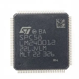
ST10F276Z5T3 - 16-Bit 40MHz MCU 832KB Flash LQFP-144 | STMicroelectronics
N.º da peça: ST10F276Z5T3 ✗ Fim de vida| Qtd. | Preço unitário | Total |
|---|---|---|
| 1 | $48.4 | $48,40 |
| 10 | $45.2 | $452,00 |
| 100 | $41.85 | $4.185,00 |
| 500 | $38.5 | $19.250,00 |
| 1.000 | $35.9 | $35.900,00 |
ST10F276Z5T3 Visão geral
A microcontroller (MCU) is an integrated circuit that combines a CPU core, program and data memory, peripherals, and I/O on a single die. The ST10 family belongs to the CISC/RISC hybrid 16-bit MCU segment, sitting hierarchically above 8-bit MCUs (8051) and below 32-bit ARM Cortex-M MCUs in embedded processing taxonomy. ST10F276Z5T3 includes a CAN on-chip programmable CAN 2.0B interface, making it part of the broader embedded microcontrollers -> microcontrollers -> embedded processors and controllers -> integrated circuits hierarchy of electronic components. Its CISC/RISC architecture balances deterministic interrupt latency with DSP-class arithmetic throughput.
Key differentiating features include the hardware MAC unit enabling single-cycle 16-bit multiplication, the 832 KByte Flash for application storage, and an integrated CAN 2.0B controller. The 144-pin LQFP package provides generous I/O count suitable for automotive body, chassis, and industrial control applications. The device supports single 5 V supply operation, with on-chip voltage regulation supporting both 5 V and 3.3 V I/O. Programming is supported via the bootstrap loader and standard JTAG/OCDS debug.
Typical applications include automotive body controllers, industrial automation PLCs, motor control, HVAC systems, and CAN-connected sensor hubs where deterministic real-time response is required. The MAC unit accelerates field-oriented control (FOC) loops in motor drives, while the large Flash/RAM ratio supports protocol stacks such as J1939 or CANopen at the application layer.
When designing with the ST10F276Z5T3, ensure proper decoupling on the 5 V rail with bulk plus 100 nF ceramic capacitors adjacent to each supply pair, and follow STMicroelectronics AN2409 PCB layout guidelines for EMC compliance on automotive platforms. Note that ST officially marks the device as NRND - prefer the ST10F276Z5T6 or STM32F3 series for new designs.
This page synthesizes distributor pricing, same-family drop-in alternatives, and practical design notes not found in the manufacturer datasheet.
Alternativas drop-in para ST10F276Z5T3 — mesmo encapsulamento, compatível pino a pino. Peças de encapsulamento diferente que exigem retrabalho na PCB são excluídas.
Variantes desta série
Modelos da mesma série compatíveis como drop-in com ST10F276Z5T3 (mesmo formato e footprint) — diferindo em Package, RAM, RoHS Status, CAN Interface, Core.
Ferramenta de comparação rápida — selecione peças alternativas para comparação lado a lado:
ST10F276Z5T6
✅ Drop-In📋 Alternativa de referência (fora do catálogo)
ST10F272Z2T3
✅ Drop-In📋 Alternativa de referência (fora do catálogo)
ST10F276Z5Q3
✅ Drop-In✓ Em estoque
$18.75 / unidade
Ver ficha técnica →ST10F273M-4T3
✅ Drop-In📋 Alternativa de referência (fora do catálogo)
SAF-XC886CM-8FFI5VAC
✅ Drop-In✓ Em estoque
$4.1 / unidade
Ver ficha técnica →ST10F276Z5T3 Classificações máximas e características elétricas
| CPU Core | ST10 (16-bit CISC/RISC with DSP functions) |
| Maximum CPU Clock | 40 MHz |
| Instruction Cycle Time | 50 ns (at 40 MHz max) |
| Program Memory (Flash) | 832 KB (832K x 8) |
| RAM | Up to 68 KB |
| MAC Unit | 16-bit x 16-bit multiplier, 40-bit accumulator |
| CAN Interface | On-chip CAN 2.0B (1 channel) |
| Operating Voltage | 5 V (with on-chip 3.3 V regulator) |
| Encapsulamento | LQFP-144 |
| Contagem de pinos | 144 |
| Tipo de montagem | Surface Mount |
| Debug Interface | JTAG / OCDS |
Configuração de pinos do ST10F276Z5T3
| Pino 1 | P5.0 — Port 5 bit 0 (digital I/O) |
| Pino 2 | P5.1 — Port 5 bit 1 (digital I/O) |
| Pino 3 | P5.2 — Port 5 bit 2 (digital I/O) |
| Pino 4 | P5.3 — Port 5 bit 3 (digital I/O) |
| Pino 5 | P5.4 — Port 5 bit 4 (digital I/O) |
| Pino 6 | P5.5 — Port 5 bit 5 (digital I/O) |
| Pino 7 | P5.6 — Port 5 bit 6 (digital I/O) |
| Pino 8 | P5.7 — Port 5 bit 7 (digital I/O) |
| Pino 9 | VDD — 5 V core supply |
| Pino 10 | VSS — Ground |
| Pino 11 | P6.0 — Port 6 bit 0 / segment control |
| Pino 12 | P6.1 — Port 6 bit 1 |
| Pino 13 | P6.2 — Port 6 bit 2 |
| Pino 14 | P6.3 — Port 6 bit 3 |
| Pino 15 | P6.4 — Port 6 bit 4 |
| Pino 16 | P6.5 — Port 6 bit 5 |
| Pino 17 | P6.6 — Port 6 bit 6 |
| Pino 18 | P6.7 — Port 6 bit 7 |
| Pino 19 | P7.0 — Port 7 bit 0 (digital I/O) |
| Pino 20 | P7.1 — Port 7 bit 1 |
| Pino 21 | P7.2 — Port 7 bit 2 |
| Pino 22 | P7.3 — Port 7 bit 3 |
| Pino 23 | P7.4 — Port 7 bit 4 |
| Pino 24 | P7.5 — Port 7 bit 5 |
| Pino 25 | P7.6 — Port 7 bit 6 |
| Pino 26 | P7.7 — Port 7 bit 7 |
| Pino 27 | VDD — 5 V I/O supply |
| Pino 28 | VSS — Ground |
| Pino 29 | P8.0 — Port 8 bit 0 (CAN / digital I/O) |
| Pino 30 | P8.1 — Port 8 bit 1 (CAN / digital I/O) |
| Pino 31 | P8.2 — Port 8 bit 2 |
| Pino 32 | P8.3 — Port 8 bit 3 |
| Pino 33 | P8.4 — Port 8 bit 4 |
| Pino 34 | P8.5 — Port 8 bit 5 |
| Pino 35 | P8.6 — Port 8 bit 6 |
| Pino 36 | P8.7 — Port 8 bit 7 |
| Pino 37 | P9.0 — Port 9 bit 0 (digital I/O) |
| Pino 38 | P9.1 — Port 9 bit 1 |
| Pino 39 | P9.2 — Port 9 bit 2 |
| Pino 40 | P9.3 — Port 9 bit 3 |
| Pino 41 | P9.4 — Port 9 bit 4 |
| Pino 42 | P9.5 — Port 9 bit 5 |
| Pino 43 | P9.6 — Port 9 bit 6 |
| Pino 44 | P9.7 — Port 9 bit 7 |
| Pino 45 | VDD — 5 V supply |
| Pino 46 | VSS — Ground |
| Pino 47 | P0.0 — Port 0 bit 0 (address/data) |
| Pino 48 | P0.1 — Port 0 bit 1 (address/data) |
| Pino 49 | P0.2 — Port 0 bit 2 (address/data) |
| Pino 50 | P0.3 — Port 0 bit 3 (address/data) |
| Pino 51 | P0.4 — Port 0 bit 4 (address/data) |
| Pino 52 | P0.5 — Port 0 bit 5 (address/data) |
| Pino 53 | P0.6 — Port 0 bit 6 (address/data) |
| Pino 54 | P0.7 — Port 0 bit 7 (address/data) |
| Pino 55 | P1.0 — Port 1 bit 0 (address) |
| Pino 56 | P1.1 — Port 1 bit 1 (address) |
| Pino 57 | P1.2 — Port 1 bit 2 (address) |
| Pino 58 | P1.3 — Port 1 bit 3 (address) |
| Pino 59 | P1.4 — Port 1 bit 4 (address) |
| Pino 60 | P1.5 — Port 1 bit 5 (address) |
| Pino 61 | P1.6 — Port 1 bit 6 (address) |
| Pino 62 | P1.7 — Port 1 bit 7 (address) |
| Pino 63 | VDD — 5 V supply |
| Pino 64 | VSS — Ground |
| Pino 65 | P2.0 — Port 2 bit 0 (address) |
| Pino 66 | P2.1 — Port 2 bit 1 (address) |
| Pino 67 | P2.2 — Port 2 bit 2 (address) |
| Pino 68 | P2.3 — Port 2 bit 3 (address) |
| Pino 69 | P2.4 — Port 2 bit 4 (address) |
| Pino 70 | P2.5 — Port 2 bit 5 (address) |
| Pino 71 | P2.6 — Port 2 bit 6 (address) |
| Pino 72 | P2.7 — Port 2 bit 7 (address) |
| Pino 73 | P3.0 — Port 3 bit 0 (digital I/O) |
| Pino 74 | P3.1 — Port 3 bit 1 |
| Pino 75 | P3.2 — Port 3 bit 2 |
| Pino 76 | P3.3 — Port 3 bit 3 |
| Pino 77 | P3.4 — Port 3 bit 4 |
| Pino 78 | P3.5 — Port 3 bit 5 |
| Pino 79 | P3.6 — Port 3 bit 6 |
| Pino 80 | P3.7 — Port 3 bit 7 |
| Pino 81 | VDD — 5 V supply |
| Pino 82 | VSS — Ground |
| Pino 83 | P4.0 — Port 4 bit 0 (digital I/O) |
| Pino 84 | P4.1 — Port 4 bit 1 |
| Pino 85 | P4.2 — Port 4 bit 2 |
| Pino 86 | P4.3 — Port 4 bit 3 |
| Pino 87 | P4.4 — Port 4 bit 4 |
| Pino 88 | P4.5 — Port 4 bit 5 |
| Pino 89 | P4.6 — Port 4 bit 6 |
| Pino 90 | P4.7 — Port 4 bit 7 |
| Pino 91 | XTAL1 — Oscillator input |
| Pino 92 | XTAL2 — Oscillator output |
| Pino 93 | RSTIN — Reset input (active low) |
| Pino 94 | RSTOUT — Reset output |
| Pino 95 | NMI — Non-maskable interrupt |
| Pino 96 | VDD — 5 V supply |
| Pino 97 | VSS — Ground |
| Pino 98 | CAN_TXD — CAN transmit data |
| Pino 99 | CAN_RXD — CAN receive data |
| Pino 100 | TDI — JTAG test data in |
| Pino 101 | TDO — JTAG test data out |
| Pino 102 | TMS — JTAG test mode select |
| Pino 103 | TCK — JTAG test clock |
| Pino 104 | TRST — JTAG test reset |
| Pino 105 | BRKOUT — Breakout / OCDS signal |
| Pino 106 | BRKIN — Breakin / OCDS signal |
| Pino 107 | ALE — Address latch enable |
| Pino 108 | RD — External read strobe |
| Pino 109 | WR — External write strobe |
| Pino 110 | READY — External ready input |
| Pino 111 | VDD — 5 V supply |
| Pino 112 | VSS — Ground |
| Pino 113 | P5IN.0 — Port 5 alternate function |
| Pino 114 | P5IN.1 — Port 5 alternate function |
| Pino 115 | P5IN.2 — Port 5 alternate function |
| Pino 116 | P5IN.3 — Port 5 alternate function |
| Pino 117 | P5IN.4 — Port 5 alternate function |
| Pino 118 | P5IN.5 — Port 5 alternate function |
| Pino 119 | P5IN.6 — Port 5 alternate function |
| Pino 120 | P5IN.7 — Port 5 alternate function |
| Pino 121 | VDD — 5 V supply |
| Pino 122 | VSS — Ground |
| Pino 123 | AIN0 — Analog input channel 0 |
| Pino 124 | AIN1 — Analog input channel 1 |
| Pino 125 | AIN2 — Analog input channel 2 |
| Pino 126 | AIN3 — Analog input channel 3 |
| Pino 127 | AIN4 — Analog input channel 4 |
| Pino 128 | AIN5 — Analog input channel 5 |
| Pino 129 | AIN6 — Analog input channel 6 |
| Pino 130 | AIN7 — Analog input channel 7 |
| Pino 131 | AREF — ADC reference voltage |
| Pino 132 | AVSS — Analog ground |
| Pino 133 | AVDD — Analog 5 V supply |
| Pino 134 | VDD — 5 V supply |
| Pino 135 | VSS — Ground |
| Pino 136 | NC — Not connected (per datasheet) |
| Pino 137 | NC — Not connected (per datasheet) |
| Pino 138 | NC — Not connected (per datasheet) |
| Pino 139 | NC — Not connected (per datasheet) |
| Pino 140 | NC — Not connected (per datasheet) |
| Pino 141 | NC — Not connected (per datasheet) |
| Pino 142 | NC — Not connected (per datasheet) |
| Pino 143 | NC — Not connected (per datasheet) |
| Pino 144 | NC — Not connected (per datasheet) |
Aplicações típicas
ST10F276Z5T3 é adequado para 6 aplicaçãos: Automotive Body Control Modules, Industrial Motor Control (FOC), HVAC Climate Control Systems, CAN-Connected Sensor Hubs, Industrial PLC Controllers, Automotive Instrument Clusters.
Automotive Body Control Modules
The ST10F276Z5T3 fits automotive body controllers because its on-chip CAN 2.0B controller, 832 KB Flash, and 16-bit CPU with deterministic interrupt response support multi-node CAN networks like body electronics gateways. With 50 ns instruction cycle time, the device handles real-time lighting, window, and door control loops with sub-millisecond latency. The 5 V supply rating allows direct connection to the 12 V automotive battery via a 5 V regulator, simplifying the power tree. The 832 KB Flash accommodates full CANopen or J1939 stacks plus application firmware, while 68 KB RAM supports runtime buffers. Pin compatibility within the ST10 family preserves PCB layout for migration to the Z5T6 successor.
Recomendado
Industrial Motor Control (FOC)
The ST10F276Z5T3 suits field-oriented control of AC induction and PMSM motors thanks to its 16-bit hardware MAC unit and 40-bit accumulator, which accelerate Park/Clarke transforms and PI controllers in real time. The 40 MHz CPU clock and 50 ns cycle time support PWM frequencies up to 20 kHz with sufficient headroom for the FOC computational loop. Its 5 V I/O interfaces directly to standard gate drivers and op-amps used in three-phase inverters. The 144-pin LQFP provides the GPIO and timer count needed for multi-axis control. Designers should leverage the MAC unit for single-cycle 16-bit multiplies to maximize loop bandwidth.
Recomendado
HVAC Climate Control Systems
The ST10F276Z5T3 is well-matched to HVAC controllers because its 832 KB Flash stores multi-zone climate logic and sensor-fusion algorithms, while the 68 KB RAM supports PID parameter tables for multiple control loops. The on-chip CAN 2.0B integrates seamlessly with automotive or industrial HVAC networks for setpoint and diagnostic messaging. The 5 V analog peripherals simplify interfacing to NTC temperature sensors, pressure transducers, and valve actuators. Deterministic interrupt response from the ST10 core ensures reliable handling of safety-critical over-temperature and pressure-limit events. Designers benefit from the wide Flash headroom for future feature additions.
Recomendado
CAN-Connected Sensor Hubs
The ST10F276Z5T3 anchors industrial sensor hubs that aggregate multiple sensor inputs and publish them over CAN, thanks to its on-chip CAN 2.0B controller and the 832 KB Flash that fits CANopen or DeviceNet dictionaries plus application code. The 16-bit CPU performs moving-window averaging, min/max tracking, and threshold detection across many sensor channels at low latency. The 5 V GPIO drives both 3.3 V and 5 V sensors with on-chip voltage regulation. The LQFP-144 footprint accommodates the ADC and timer count needed for multi-channel synchronous sampling.
Recomendado
Industrial PLC Controllers
The ST10F276Z5T3 provides the deterministic execution and CAN connectivity required for compact industrial PLCs and remote I/O nodes. Its 16-bit CPU with single-cycle context switching supports fast scan times under 1 ms even with extensive ladder-logic translation. The 832 KB Flash hosts IEC 61131-3 runtimes plus user programs, while the 68 KB RAM accommodates scan buffers and stack space. The 5 V supply operates directly from 24 V industrial rails via a single regulator. Pin compatibility within the ST10F276 family enables long-term supply continuity through the Z5T6 successor.
Recomendado
Automotive Instrument Clusters
The ST10F276Z5T3 supports automotive instrument cluster MCUs where its 832 KB program memory and CAN 2.0B interface enable gauge control, warning indicators, and CAN-based data exchange with the vehicle bus. The 50 ns instruction cycle time drives segmented or dot-matrix LCDs at acceptable refresh rates without external display controllers. The 16-bit DSP-enhanced core handles filter algorithms on analog speed/RPM inputs from the CAN gateway. The 144-pin LQFP provides GPIO for backlight drivers, button inputs, and tell-tale LEDs. For new designs, recommend the ST10F276Z5T6 successor with longer-term availability.
Recomendado
Resumo dos produtos recomendados
Dados de referência de engenharia para ST10F276Z5T3 — comparação, orientação de projeto e informações de conformidade.
Guia de seleção
Comparação com alternativas
| Parâmetro | Este produto | ST10F276Z5T6 | ST10F272Z2T3 | ST10F276Z5Q3 | ST10F273M-4T3 | SAF-XC886CM-8FFI5VAC |
|---|---|---|---|---|---|---|
| Package | LQFP-144 | LQFP-144 - same | LQFP-144 - same | LQFP-144 - same | LQFP-144 - same | TQFP-48 - different |
| Brand | STMicroelectronics | STMicroelectronics | STMicroelectronics | STMicroelectronics | STMicroelectronics | Infineon Technologies |
| CPU Core | ST10 16-bit CISC/RISC | ST10 16-bit CISC/RISC | ST10 16-bit CISC/RISC | ST10 16-bit CISC/RISC | ST10 16-bit CISC/RISC | XC800 8/16-bit CISC |
| Maximum CPU Clock | 40 MHz | 40 MHz | 40 MHz | 40 MHz | 40 MHz | 24 MHz |
| Flash Memory | 832 KB | 832 KB | 512 KB | 832 KB | 832 KB | 32 KB |
| RAM | Up to 68 KB | Up to 68 KB | Up to 40 KB | Up to 68 KB | Up to 68 KB | 2 KB |
| CAN Interface | CAN 2.0B (1 channel) | CAN 2.0B (1 channel) | CAN 2.0B (1 channel) | CAN 2.0B (1 channel) | CAN 2.0B (1 channel) | CAN (1 channel) |
| Operating Voltage | 5 V (with on-chip 3.3 V regulator) | 5 V (with on-chip 3.3 V regulator) | 5 V (with on-chip 3.3 V regulator) | 5 V (with on-chip 3.3 V regulator) | 3.3 V | 5 V |
| Lifecycle Status | NRND | Active (recommended replacement) | NRND | NRND | NRND | Mature |
Principais diferenciais
- Largest on-chip Flash in ST10 family (vs ST10F272Z2T3)
- 5 V native I/O for automotive battery-direct design (vs ST10F273M-4T3)
- Hardware 16-bit MAC unit for DSP-class math (vs SAF-XC886CM-8FFI5VAC)
Notas de projeto
The ST10F276Z5T3 requires a clean 5 V supply with bulk capacitance of at least 10 uF low-ESR tantalum or ceramic plus 100 nF ceramic placed within 5 mm of each VDD pin pair. Estimated: assuming typical switching currents of 100 mA in digital I/O, expect <50 mV supply ripple. Use a ferrite bead on the 5 V rail feeding the analog AVDD pin to prevent digital switching noise coupling into ADC conversions.
The LQFP-144 package has theta_JA around 50 C/W typical on a 4-layer JEDEC test board. Estimated: at 40 MHz full operation with all peripherals active, the device may dissipate up to 1.0 W. Derate at ambient temperatures above 85 C by ensuring adequate PCB copper area (at least 2 square inches of ground pour) or consider forced-air cooling for industrial -40 to +125 C environments.
Per the STMicroelectronics datasheet, the RSTIN pin must be held low for at least 1024 oscillator cycles during power-up to ensure proper initialization. Bootstrap loader mode is entered by pulling specific pins (P0L.4, P0L.5) high during reset. Do not leave unused ADC inputs floating - tie them to ground to prevent ADC channel crosstalk. Always issue a software reset before jumping to user code after programming to clear residual peripheral state.
Follow STMicroelectronics application note AN2409 PCB layout recommendations for EMC compliance on automotive platforms. Place the 5 V decoupling capacitors as close as possible to each VDD/VSS pin pair with short, wide traces. Use a single ground plane split only between analog AVSS and digital VSS at one point under the device. Route the CAN differential pair (CAN_TXD, CAN_RXD) as a 100-ohm impedance matched pair with no stubs. The crystal oscillator traces should be kept short and surrounded by ground pour.
Informações de conformidade
Compliance status not explicitly stated in the verified web data. Refer to the STMicroelectronics product page or contact ST directly for current RoHS, REACH, and lead-free declarations. The standard variant is not AEC-Q100 qualified; check the ST10F276 automotive-grade variant for AEC-Q100 status.