CIs de Interface
Subcategorias
Produtos (1151)

MCP2515-I/SO - Stand-Alone CAN 2.0B Controller w/ SPI | Microchip
The Microchip Technology MCP2515-I/SO is a stand-alone Controller Area Network (CAN) protocol controller that implements the CAN specification version 2.0B, housed in an 18-pin SOIC (SO) package with -40C to +125C industrial temperature rating. It communicates with a host microcontroller through an industry-standard Serial Peripheral Interface (SPI) at up to 10 MHz clock, and supports CAN bit rates up to 1 Mb/s. A CAN controller is a dedicated hardware block that implements the ISO 11898-1 data-link layer, offloading bit-stuffing, CRC generation, arbitration, error handling, and acceptance filtering from the host MCU. As part of the controller IC hierarchy, the MCP2515 sits below the CAN transceiver (e.g., MCP2551, TJA1050) which handles the physical layer, and below the full CAN protocol stack running on microcontrollers. It is a member of the interface IC family, bridging a digital MCU to a 2-wire differential CAN bus. Key features of the MCP2515 include two acceptance masks and six acceptance filters (29-bit extended and standard 11-bit IDs), two receive buffers with prioritization, three transmit buffers with prioritization and abort capability, hardware support for time-triggered protocols (CANopen, DeviceNet), and byte-level data filtering. The part offers both 5V and 3.3V operation with low standby current, supports one-shot mode for retransmission control, and provides an interrupt output for event-driven MCU wake-up. The MCP2515 is pin- and function-compatible with the older MCP2510, adding faster SPI throughput (10 MHz vs 5 MHz), databyte filtering, and time-triggered protocol support. The internal architecture pairs a CAN protocol engine with two acceptance masks, a 6-filter hardware acceptance filter array, an SPI engine with command-based register access, and flexible interrupt logic that signals MCU-side events via the INT pin. Typical applications include automotive body and chassis networking, industrial CANopen and DeviceNet nodes, HVAC and elevator controllers, building automation, and Arduino/Raspberry Pi CAN shields. When designing with the MCP2515, pair it with a CAN transceiver (e.g., MCP2551, TJA1050) to convert CMOS TXCAN/RXCAN to the differential bus; without that companion chip the controller cannot drive a real CAN bus. One important design consideration is the SPI clock and MCU timing budget - while the controller supports up to 10 MHz SPI, the actual achievable bus throughput depends on host MCU SPI peripheral speed, interrupt latency, and buffer-drain handling. Designers should also handle bus-off recovery by software, since the MCP2515 does not auto-recover from bus-off without host intervention. This page synthesizes distributor pricing, drop-in same-family and cross-brand replacements, and practical design guidance not bundled in the manufacturer datasheet itself.

MCP2517FD-H/SL - 8 Mbps CAN FD SPI Controller | Microchip
The Microchip Technology MCP2517FD-H/SL is an external CAN FD controller with an SPI interface, CAN 2.0 compatibility, data rates up to 8 Mbps, and a 14-pin SOIC package. It adds a CAN FD channel to a microcontroller that already provides SPI, avoiding the need for a processor with an integrated CAN controller. The verified distributor listing identifies the device as a CANbus controller with a CAN 2.0 SPI interface and 14-SOIC package. A CAN FD controller is a protocol-specific semiconductor that organizes arbitration frames, data frames, bit timing, error handling, interrupts, and transmit buffers. It operates above the physical-layer transceiver in the CAN node hierarchy: microcontroller, MCP2517FD controller, CAN transceiver, and bus. This controller requires an external transceiver such as the ATA6563 used on Microchip's MCP2517FD Click board; CAN RXD and CAN TXD are controller-side signals, not direct bus connections. Verified features include a 2.7 V to 5.5 V supply range, automatic retransmission control, monitor mode, and low-power mode. Automatic retransmission supports recovery from failed transmissions, while monitor mode permits observation without normal participation. Low-power mode can reduce activity when the network is idle, although the complete node power budget also depends on the MCU, SPI activity, clock source, and external transceiver. The SPI host interface makes the controller suitable for industrial automation, automotive electronics, transportation systems, medical equipment, robotics, and embedded gateways. The CAN FD architecture supports migration from classic CAN while retaining efficient handling of higher-bandwidth payloads. Firmware must initialize bit timing, configure GPIO and interrupt behavior, select arbitration versus data-phase bit rates, and manage the controller's message objects. PCB placement requires short SPI traces, a clean ground reference, careful decoupling, and separation from high-energy transceiver and bus routing. The controller and transceiver should share a compatible ground reference, while CANH and CANL routing should remain tightly coupled. Power and signal integrity depend on component placement, loop area, supply impedance, and the external transceiver implementation. This page combines verified manufacturer and distributor information, procurement data, application guidance, and replacement analysis. Because the supplied sources do not expose complete electrical tables, timing limits, pin functions, or a qualified drop-in equivalent list, unsupported details are explicitly marked rather than inferred.
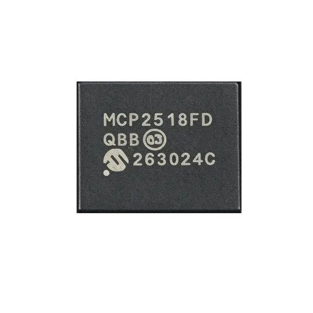
MCP2518FDT-E/QBB - CAN FD Controller, SPI, 14-VDFN | Microchip
The Microchip Technology MCP2518FDT-E/QBB is a stand-alone, low-power External CAN FD Controller with an SPI interface, housed in a 14-pin VDFN (4.5 mm x 3 mm) package with wettable flanks for automated optical inspection. It supports both Classical CAN 2.0B and CAN Flexible Data Rate (CAN FD) frames, enabling a cost-effective upgrade path for legacy CAN networks while delivering the higher payload and bit-rate advantages of CAN FD. The device integrates ECC-protected 2 KB RAM, dual maskable interrupt outputs, and grade-1 automotive temperature rating (-40C to +125C). A CAN FD Controller is a peripheral IC that handles the CAN/CAN FD protocol layer independent of the host microcontroller, exposing the bus as a register-mapped SPI slave. In the broader hierarchy, it sits above the physical-layer transceiver (such as the MCP2562FD) and below the application MCU; together these three blocks form a complete ISO 11898-1:2015 CAN node. Using an external controller lets designers add CAN FD to MCUs lacking an integrated CAN module, or offload protocol processing from low-power microcontrollers. Key features of the MCP2518FDT-E/QBB include up to 1 Mbit/s nominal CAN FD bit rate, 8 Mbit/s SPI clock support, low-power mode drawing approximately 10 µA typical, time-stamping via 32-bit TMR, and a wide operating voltage range of 2.7 V to 5.5 V. The VDFN-14 package occupies only 13.5 mm^2 of board area, making it the smallest CAN FD controller in Microchip's portfolio and ideal for space-constrained ECUs and sensor nodes. Architecturally, the MCP2518FD uses a dedicated CAN FD protocol engine plus RAM buffers, freeing the host MCU from bit-stuffing, arbitration, and CRC calculation. The SPI interface supports mode 0 and mode 3, with standard read/write commands plus a 16-bit CRC option on critical registers for EMI robustness. Combined with the external MCP2562FD high-speed transceiver, the resulting node is ISO 11898-1:2015 and ISO 11898-2:2016 compliant. Typical applications include automotive body and chassis networks, industrial CAN nodes (sensor hubs, motor drives), EV battery management (BMS) daisy chains, agricultural and off-highway vehicle telemetry, and any MCU-based system retrofitting CAN FD. The grade-1 (-40C to +125C) qualification makes it suitable for under-hood and chassis-mounted ECUs. When designing with this device, ensure the VDFN-14 exposed pad is soldered to a sufficiently large ground copper pour for thermal dissipation. A 100 nF decoupling capacitor must be placed within 5 mm of the VDD pin. The oscillator start-up time depends on the crystal load capacitance; consult the Microchip datasheet for matching network values. This page synthesizes distributor stock levels, parametric drop-in alternatives (including same-package Microchip variants), and PCB-layout guidance that is not consolidated on any single manufacturer or distributor product page.

MCP2551-E - 1Mb/s High-Speed CAN Transceiver, ISO-11898 | Microchip
The Microchip Technology MCP2551-E is a high-speed, fault-tolerant CAN (Controller Area Network) transceiver that serves as the physical-layer interface between a CAN protocol controller and the differential CAN bus, capable of operating at data rates up to 1 Mb/s and fully compliant with the ISO-11898 standard including 24V bus requirements, housed in an 8-pin SOIC (SN) package. The device provides differential transmit and receive capability for the CAN protocol controller, with a single 5V supply input (4.5V to 5.5V), an internal slope-control pin for selectable baud-rate modes, and a low-power standby mode current of roughly 275 µA typ. A CAN transceiver is the analog physical-layer bridge of any CAN bus, sitting between a digital CAN controller (such as the MCP2515) and the actual twisted-pair wiring harness. Its primary job is to translate the controller's TXD/RXD CMOS logic into the dominant/recessive differential voltage levels defined by ISO-11898, while absorbing ESD strikes, bus shorts, and load-dump transients so the fragile controller is never exposed to them. As a category, CAN transceivers fall under interface ICs in the broader semiconductor taxonomy of standard logic and bus-interface devices. Key features of the MCP2551-E include three operating modes (high-speed, slope-control for lower EMI, and standby) selected via the RS pin, a transmitter capable of driving a worst-case 45-Ω load (corresponding to a heavily-loaded bus with 64 nodes), automatic thermal-shutdown protection, and bus fault tolerance meeting the 24V automotive requirement. The VREF pin supplies a 0.5 × VCC reference useful for stabilizing the recessive level. Architecturally, the die uses a bipolar driver stage for robust bus-side drive strength, with CMOS logic on the controller-side pins. The driver's output impedance and the on-chip slope-control current source are trimmed at the wafer level to give predictable rise/fall times across temperature, which is important in automotive under-hood environments where the bus length and capacitance can vary widely. Typical applications include in-vehicle networking (OBD-II, body controllers, instrument clusters), industrial CANopen and DeviceNet links, and any 5V microcontroller system needing a standard ISO-11898 CAN port. Designers often pair the MCP2551-E with the MCP2515 controller (the same Microchip family) for a complete CAN node. When designing with the MCP2551-E, always place a 100 nF decoupling capacitor close to VCC and provide a common-mode choke plus a 120 Ω termination resistor at each end of the bus. The part is now being superseded by the AEC-Q100-qualified MCP2561 for new automotive designs, but remains widely available and fully supported for industrial and legacy systems. This page consolidates Microchip datasheet specifications, drop-in SOIC-8 alternatives such as the MCP2561 and TI SN65HVD251, and field-level design guidance not found in a quick distributor lookup.

MCP2551-E-P - 1 Mbps Fault-Tolerant CAN Transceiver
The Microchip Technology MCP2551-E-P is a 1 Mbps high-speed CAN physical-layer transceiver with one transmitter and one receiver, a 4.5 V to 5.5 V supply range, and an 8-pin DIP package. It provides the physical interface between a CAN protocol controller and the differential CAN bus while supporting fault-tolerant operation in 12 V and 24 V systems. According to the supplied data, it implements ISO-11898 physical-layer requirements and uses externally controlled slope to reduce radio-frequency interference. A CAN transceiver is an interface IC that converts logic-level controller signals into the differential physical signaling used by a Controller Area Network. The MCP2551-E-P belongs to the hierarchy CAN transceiver > bus interface > interface IC > semiconductor. This device combines a CAN driver, CAN receiver, bus-fault handling, standby control, and a reference output in one physical-layer device. Its principal features include 1 Mb/s operation, one driver and one receiver, 4.5 V to 5.5 V operation, and suitability for 12 V and 24 V systems. Externally controlled slope is especially useful when electromagnetic compatibility must be balanced against bus timing. Fault tolerance is a core function because automotive and industrial CAN buses can experience wiring faults and abnormal bus conditions. The MCP2551-E/P designation identifies the through-hole 8-pin DIP format in the supplied distributor data. It is intended for designs using a CAN controller with a logic-side interface and a differential CANH/CANL bus connection. The package and protocol role make it relevant to automotive electronics, industrial automation, robotics, embedded control, and instrumentation. A key design consideration is that CAN bus implementation depends on correct termination, common-mode behavior, transceiver wiring, controller compatibility, and PCB or harness layout. The verified search data identifies the device as fault tolerant and capable of 1 Mb/s operation, but detailed loop-delay, propagation-delay, receiver-threshold, and absolute-maximum-rating values were not supplied. Those values should be taken from the manufacturer datasheet before final timing or protection design. This page synthesizes the supplied distributor and manufacturer-search data, package information, CAN use cases, replacement considerations, and practical design guidance. It does not infer undocumented electrical limits or assume regulatory compliance.
MCP2551-E/SN - High-Speed CAN Transceiver 1Mbps SOIC-8 | Microchip
The Microchip Technology MCP2551-E/SN is a high-speed CAN (Controller Area Network) transceiver in an 8-pin SOIC (SN) package, providing the physical interface between a CAN protocol controller and the differential bus. It supports data rates up to 1 Mbps and is fully compatible with the ISO-11898-24V standard, including 24V bus fault protection. Operating from a single 4.5V to 5.5V supply, it is a 1/1 (one transmitter, one receiver) half-duplex transceiver. A CAN transceiver is the analog physical-layer device that converts the digital TX/RX logic signals from a CAN controller (such as the MCP2515) into the differential voltage levels required on a CAN bus. The CAN protocol itself is defined by ISO 11898 and is widely used in automotive (CAN, CAN-FD), industrial (CANopen, DeviceNet), and medical equipment because of its robust differential signaling, built-in arbitration, and reliable behavior in electrically noisy environments. Transceivers like the MCP2551 sit in the hierarchy: physical-layer transceiver -> CAN controller -> host MCU -> application layer. Key features include slope control for reduced EMI (selectable via the RS pin), a low-power standby mode (pin S1), thermal shutdown protection, short-circuit protection on the bus pins (CANH/CANL) to battery and ground, and an internal VREF output for biasing split termination. The device survives load-dump events up to ±40V on the bus pins, exceeding the ISO-7637 transient specification. Up to 112 nodes can be connected to a single CAN bus segment. Typical applications include automotive body and chassis networks, industrial CANopen and DeviceNet nodes, building automation (BACnet), fleet management and telematics, and any embedded system that needs ISO-11898-compliant differential CAN communication. The 5V VCC and 8-pin SOIC footprint also make it a convenient drop-in upgrade for legacy MCP2551 designs being migrated to longer lead-time alternatives. When designing with this device, place a 100nF decoupling capacitor close to VCC and use a split termination network (typically 120 ohm total with two 60 ohm resistors and a 10nF capacitor to ground) to match the bus impedance and suppress common-mode noise. Ensure the RS pin is tied to ground for high-speed mode or through a resistor to slow the slew rate if EMI is a concern.
MCP2551-I - High-Speed CAN Transceiver, 1 Mb/s, 8-Pin DIP/SOIC | Microchip
The Microchip Technology MCP2551-I is a high-speed CAN (Controller Area Network) fault-tolerant transceiver that interfaces a CAN protocol controller to the physical bus, operating at data rates up to 1 Mb/s in an 8-pin PDIP or SOIC package. It provides differential transmit and receive capability, is fully compatible with the ISO-11898 standard, and meets the 24V automotive bus requirement. The device supports a supply voltage range of 4.5V to 5.5V and is designed for harsh industrial and automotive environments. A CAN transceiver is a physical-layer device that translates the digital transmit/receive signals from a CAN controller into the differential voltage levels (CANH/CANL) required on the bus. It belongs to the broader hierarchy of interface ICs, sitting between protocol controllers (such as MCP2515 standalone CAN controllers) and the physical wiring harness, and ultimately forms part of the in-vehicle or industrial networking infrastructure. CAN transceivers like the MCP2551-I are the bedrock of automotive OBD-II, CANopen, and DeviceNet networks. Key features include ±80V bus fault protection on CANH and CANL, a high-noise immunity design (>1V common-mode range), thermal shutdown protection, and an automatic thermal slope control that reduces emissions at lower data rates. The device has three operating modes: High-Speed, Slope-Control, and Standby, with the mode selected via the RS pin. A VREF output (2.5V typical) is provided as a voltage reference for the CAN controller. The MCP2551-I uses a bipolar process technology and incorporates slope control to minimize EMI by limiting the rise/fall times of CANH and CANL. Its differential receiver provides excellent noise immunity with a typical hysteresis of 100 mV. The transceiver operates across -40°C to +125°C industrial temperature range, making it suitable for under-hood automotive and rugged industrial applications. Typical applications include automotive body and chassis networks, industrial CANopen and DeviceNet nodes, OBD-II vehicle diagnostics, HVAC and elevator control systems, and medical instrumentation interconnects. Designers frequently pair the MCP2551-I with the MCP2515 standalone CAN controller for full CAN node implementations. A critical design consideration is bus termination: the CAN bus requires 120 Ω resistors at each end of the bus segment, and these are typically not integrated in the MCP2551-I. The RS pin should be tied high through a resistor to VCC for high-speed operation or connected to ground through a resistor to enable slope-control mode for lower EMI at reduced data rates. This page synthesizes distributor pricing, drop-in alternatives, and practical design notes not found in the manufacturer datasheet alone, including cross-brand equivalents and pin-compatible migration paths to the MCP2561.
MCP2551-I/P - 5V High-Speed CAN Transceiver DIP-8 | Microchip
The Microchip MCP2551-I/P is a high-speed CAN (Controller Area Network) protocol transceiver in an 8-pin PDIP (P) package, operating from a 4.5V to 5.5V single supply. It provides differential transmit and receive capability between a CAN protocol controller and the physical two-wire bus, supporting data rates up to 1 Mb/s per ISO-11898. The device includes slope-control input for selectable high-speed or slope-controlled (lower EMI) operation, a standby pin for low-power mode, and a VREF output for internal reference. A CAN transceiver is a physical-layer interface IC that bridges a digital CAN controller (typically a microcontroller with a CAN module) and the differential CAN bus wiring. It converts single-ended TXD logic into differential bus voltages on transmit, and converts differential bus voltages back into single-ended RXD logic on receive. CAN transceivers are the physical foundation of robust in-vehicle networking and industrial fieldbuses, and they are governed by the ISO 11898 family of standards. Key features of the MCP2551-I/P include: 1/1 (one driver, one receiver) half-duplex topology, 200 mV receiver hysteresis for noise immunity, thermal shutdown protection, short-circuit protection to battery and ground on the bus pins (up to ±40 V), and an operating temperature range of -40C to +85C (the "I" industrial grade). The device is widely deployed in automotive ECUs, industrial CAN nodes, building automation, and any embedded system that requires ISO 11898 compliant physical-layer connectivity. The MCP2551-I/P uses a bipolar architecture with internal slope control to limit EMI from the bus driver edge rates. The receiver inputs feature high common-mode range so the part tolerates ground offset between nodes. In addition, the device includes a VREF pin for a stable mid-supply reference voltage that older controllers require, making it a backwards-compatible choice for legacy CAN designs. Typical applications include automotive body and chassis ECUs, industrial CANopen and DeviceNet nodes, OBD-II diagnostic interfaces, agricultural machinery networks, and elevator or building automation controllers. Because the part is in a through-hole PDIP-8 package, it is also commonly used in prototyping, education kits, and hobby robotics (e.g. Arduino CAN shields) where through-hole assembly is preferred. When designing with the MCP2551-I/P, observe ISO 11898 bus termination requirements: a 120 ohm termination resistor at each end of the bus, twisted-pair cabling, and adequate common-mode choke or ESD protection for harsh environments. Also note that Microchip's newer MCP2561/2 family is the recommended migration path for new designs. This page synthesizes distributor pricing, drop-in alternatives, and practical design notes not found in the manufacturer datasheet.
MCP2551-I/SN - High-Speed CAN Transceiver, 1Mb/s, ISO-11898 | Microchip
The Microchip Technology MCP2551-I/SN is a high-speed Controller Area Network (CAN) protocol transceiver that serves as the interface between a CAN protocol controller and the physical differential bus, operating at speeds up to 1 Mb/s. The device is supplied from a single 4.5 V to 5.5 V rail, packaged in an 8-pin SOIC (SN) with industry-standard pinout, and provides differential transmit and receive capability to the bus. It is fully compatible with the ISO-11898 standard physical-layer requirements, including the 24 V load specification, making it suitable for both 12 V and 24 V automotive and industrial systems. A CAN transceiver is a physical-layer (PHY) device that converts the single-ended TTL-level transmit (TXD) and receive (RXD) signals of a CAN controller into the differential CAN_H and CAN_L signals driven on the bus. Transceivers such as the MCP2551 provide the dominant/recessive arbitration signaling, bus biasing, ESD protection, and fault tolerance needed by the differential multi-drop CAN bus used in automotive and industrial networking. They sit between the bus and protocol controllers such as the Microchip MCP2515 or the MCU-integrated CAN modules on dsPIC, PIC18, and many ARM Cortex-M microcontrollers. Key features of the MCP2551-I/SN include 1 Mb/s maximum data rate, externally-controlled slope (rise/fall) adjustment for reduced RFI, a low-current standby mode, a VREF output for the CAN controller's input reference, and detection of permanent bus dominant faults with automatic recovery to receiver-only mode. The device also supports the -2 V to +7 V common-mode range required by ISO-11898-2 (extended common-mode versions go further) and includes thermal shutdown and current limiting on the bus pins for bus-fault protection. Architecturally, the MCP2551 uses an NMOS differential driver on the bus side with slope control implemented by varying the driver output current; a bandgap-based VREF generator provides a 2.5 V (typical) reference for the RXD comparator threshold generation inside the controller. Internal hysteresis and input filtering suppress RF and transient noise on CAN_H/CAN_L without delaying the bit time, which preserves CAN arbitration timing at the maximum 1 Mb/s data rate. Typical applications include automotive body and powertrain networks, industrial CAN-based control systems (CANopen, DeviceNet, NMEA 2000), building automation, HVAC controls, and any embedded design using a Microchip MCU with a CAN module. Its 8-SOIC footprint and 5 V supply make it easy to add a CAN physical layer to existing 5 V designs. Note: per Microchip's discontinuance notices, the MCP2551 in SOIC-8 (SN) is being phased out, so verify stock and review the recommended MCP2561/2562 successor family for new designs. When designing with this device, observe CAN bus termination: place 120 ohm resistors at each END of the bus (not at every node), and use twisted-pair cabling. Provide a small decoupling capacitor as close as possible to VDD (pin 3) and tie the unused RS pin (pin 8) to GND through a resistor (or directly) to select normal high-speed slew rate. This page synthesizes distributor pricing, drop-in alternatives, and practical PCB/CAN-bus design notes not found in a single manufacturer datasheet.
MCP2562-E/SN - 1Mbps CAN Transceiver, 5V | Microchip
The Microchip Technology MCP2562-E/SN is a 1 Mbps high-speed CAN transceiver with a 4.5 V to 5.5 V supply range and an 8-pin SOIC package. It provides one CAN transmitter and one CAN receiver, bridging a CAN protocol controller to a physical two-wire CAN bus. A dedicated VIO supply supports direct interfacing with microcontrollers operating from 1.8 V to 5.5 V. A CAN transceiver is an interface IC that converts logic-level controller signals into the dominant and recessive voltage states used on a CAN bus, while converting bus states back into controller-compatible receive data. The MCP2562 family is commonly used in the CAN interface layer between a host microcontroller, CAN controller, vehicle network, industrial automation system, or embedded diagnostic equipment. The verified product information identifies the MCP2562-E/SN as a 1 Mbps CAN transceiver with a 5 V operating supply and an 8-pin SOIC package. Its separate VIO pin reduces the need for external level shifters when the CAN controller uses a lower-voltage IO domain. The device also supports standby control and undervoltage-related bus-management functions according to the product description sources. The MCP2562-E/SN is suitable for high-speed CAN networks requiring a compact surface-mount solution. Its 1 Mbps data rate supports automotive and industrial communication systems, while the dedicated VIO supply helps simplify connections to modern low-voltage microcontrollers. The 8-SOIC package also facilitates conventional PCB assembly and inspection. Typical applications include automotive engine-control modules, body electronics, industrial controllers, robotics, CAN-based sensor networks, diagnostic equipment, and embedded communication gateways. Designers should verify pin compatibility, transceiver mode behavior, supply sequencing, bus termination, and EMC requirements before replacing another CAN transceiver. This page combines verified distributor and manufacturer-derived product facts, structured specifications, application guidance, design notes, and same-footprint alternatives. Exact operating-temperature limits, loop-delay values, ESD ratings, and pin-level electrical limits require confirmation from the manufacturer datasheet before design release.
MCP2562FD-E/SN - CAN FD Transceiver, 8-SOIC | Microchip
The Microchip Technology MCP2562FD-E/SN is a second-generation high-speed CAN Flexible Data Rate (CAN FD) transceiver that interfaces a CAN protocol controller to the physical two-wire CAN bus, housed in an 8-pin SOIC (SN) package. It supports data rates up to 8 Mbps in CAN FD mode, 5 Mbps in classic CAN mode with high-speed slew rate, and operates over a VIO supply range of 1.8V to 5.5V for direct MCU interface. Key features include a maximum loop delay of 130 ns and guaranteed loop delay symmetry to support CAN FD bit timing requirements. The device operates across an ambient temperature range of -40C to +125C and survives load dump transients up to +/- 70V on the bus pins through integrated protection. A CAN transceiver serves as the physical-layer interface between a CAN protocol controller (such as the MCP2518FD or integrated CAN module on a microcontroller) and the differential CAN bus (CANH/CANL). It translates the controller's transmit (TXD) and receive (RXD) digital logic into the differential bus signaling defined by ISO 11898-2:2016, and provides the dominant and recessive states needed for non-destructive bitwise arbitration. CAN FD extends the classic CAN payload from 8 bytes to 64 bytes while remaining backward-compatible at the physical layer, which is why FD-compliant transceivers like the MCP2562FD are now preferred even for classic CAN designs. The MCP2562FD delivers 5 key advantages. First, the integrated VIO pin eliminates level shifters when interfacing 1.8V/3.3V MCUs. Second, low loop-delay symmetry (<=130 ns total) enables reliable 2 Mbps and 5 Mbps CAN FD operation. Third, +/- 36V receiver common-mode range tolerates large ground shifts across nodes. Fourth, +/- 70V bus-pin transient protection (IEC 61000-4-2 ESD and load dump) eliminates external TVS diodes in most automotive 12V/24V systems. Fifth, an ultra-low-current standby mode (~15 uA typical) preserves battery life in always-bus-wake applications. The MCP2562FD uses a 1.8V to 5.5V VIO supply rail that sets the logic level reference for TXD, RXD, and the standby (STBY) pin, while the VCC/VSUP rail (4.5V to 5.5V) powers the bus-side driver. An on-chip LDO from VCC to VIO is provided on the -H variants; the -E/SN variant requires the user to supply VIO externally for maximum flexibility. The integrated slope-control circuitry automatically adjusts the CANH/CANL edge rate to meet ISO 11898-2:2016 at any speed between 50 kbps and 5 Mbps, so no external resistor selection is required. Typical applications include automotive gateway ECUs, body-control modules, ADAS sensor CAN buses, industrial PLC networking, agricultural machinery CAN backbones, and any battery-powered remote sensor that needs an always-listening low-power mode. It also suits prototypes and maker projects using boards such as the Teensy, Arduino, and Raspberry Pi that need a CAN shield with simple 3.3V logic. When designing with this device, route the CANH/CANL traces as a 120-ohm differential pair with characteristic impedance of 120 ohms and place a 120-ohm termination resistor at each end of the bus; place a 100 nF decoupling capacitor as close as possible to the VCC and VIO pins to suppress switching noise from the bus driver. This page synthesizes distributor pricing, drop-in cross-brand alternatives, and practical layout guidance not found in the manufacturer datasheet.

MCP4162-503E/MS - 50kΩ SPI Digital Potentiometer | Microchip
The Microchip Technology MCP4162-503E/MS is a single, non-volatile 8-bit digital potentiometer with a 50kΩ end-to-end resistance, 257 wiper positions, a four-wire SPI interface, and an 8-pin MSOP package. It combines a digitally controlled resistor with EEPROM-backed wiper storage, allowing a microcontroller to set and retain an analog resistance without a mechanical adjustment. A digital potentiometer is a programmable passive-network component that replaces a conventional mechanical potentiometer. Its internal resistor array provides two terminals and a wiper terminal, while an external controller moves the wiper through discrete codes. Digital potentiometers belong to the broader analog-control IC and programmable-resistor categories and are commonly used for gain, offset, filtering, sensing, and calibration circuits. The MCP4162-503E/MS provides 257 selectable wiper positions, corresponding to 8-bit control resolution and a nominal 50kΩ resistance. Its SPI-compatible serial interface supports digital setting from a host controller, while the non-volatile memory preserves the programmed wiper value for subsequent power cycles. The device is identified by verified distributor data as a single-circuit digital potentiometer in an 8-MSOP package. The -503E/MS ordering code denotes the 50kΩ resistance option and the MS package variant. The E designation is associated with the extended operating-temperature option in common Microchip digital-potentiometer naming, although the exact temperature limits and electrical tolerances should be confirmed in the manufacturer datasheet before production release. The part uses a four-wire SPI interface with chip select, serial clock, serial data input, serial data output, and power pins in the 8-pin package. Typical applications include programmable amplifier gain stages, sensor-signal conditioning, audio volume or attenuation control, industrial calibration networks, and embedded systems requiring persistent control settings. Because the MCP4162-503E/MS stores its wiper value in non-volatile memory, it is useful when the system must restart without losing a calibration or user-adjustment value. Designers should verify the complete pinout, electrical limits, wiper resistance, memory endurance, and timing characteristics against the Microchip MCP4162 datasheet. Place the device close to the controlled analog network, keep SPI traces away from sensitive high-impedance nodes, and confirm that the selected resistance and wiper current suit the application. This product page combines verified distributor information, package data, replacement guidance, and practical selection notes for engineers evaluating the MCP4162-503E/MS.

MCZ33287EG - Contact Monitor + Dual Low-Side Driver SOIC-20
The NXP MCZ33287EG is a Contact Monitoring and Dual Low-Side Protected Driver interface IC housed in a 20-pin SOIC (0.295 inch, 7.50 mm width) package. It integrates eight switch-contact monitor inputs that can be configured for switch-to-battery or switch-to-ground sensing, plus two internal low-side protected driver outputs for direct solenoid or relay actuation. The part is specified for the automotive temperature range and is lead-free / RoHS compliant. An automotive contact monitor (sometimes called a switch-contact interface IC) is a specialized power-management and signal-conditioning device that sits between the low-voltage digital domain of a microcontroller and the harsh, transient-rich electrical environment of an automobile body controller. In modern vehicles, dozens of mechanical switches (door latches, window position sensors, seat switches, headlamp controls) must be reliably debounced, level-shifted, and translated into logic-level signals that a microcontroller can read, even in the presence of conducted EMI, reverse-battery events, and load-dump transients. The category hierarchy is: contact monitor / switch interface IC -> peripheral driver -> interface IC -> power management & signal conditioning -> semiconductor. Key features include eight configurable contact-sense inputs, two low-side protected drivers with built-in thermal shutdown, automotive-grade temperature rating, and gull-wing SO-20 leads compatible with standard reflow and wave-solder processes. The IC operates from a wide supply range and includes internal clamping and protection structures on both the inputs and outputs. Compared with discrete resistor networks and external MOSFET drivers, the MCZ33287EG collapses significant BOM count, simplifying automotive body-controller PCBs. Internally, the contact monitor block combines programmable current sources, comparators with adjustable thresholds, and debounce timers; the dual low-side driver uses on-chip N-channel MOSFETs with thermal and short-circuit protection. The integrated protection eliminates the need for external flyback diodes on inductive loads such as relays and small solenoids, reducing both board area and BOM cost. Typical applications include automotive body controllers reading door, window, seat, and lighting switches; HVAC control modules that need to monitor multiple contact closures; central locking and alarm systems driving relays and small actuators; and industrial PLCs where robust switch monitoring with protected outputs is required. The part was originally launched by Freescale Semiconductor, now NXP. When designing with the MCZ33287EG, ensure adequate copper area for thermal dissipation on the low-side driver outputs (especially at full continuous current into inductive loads) and follow the datasheet recommendations for input RC filtering to suppress high-frequency EMI from automotive wiring harnesses. This page synthesizes distributor pricing, verified drop-in alternatives, and practical design notes not found in the manufacturer datasheet, helping engineers shorten sourcing and qualification cycles for automotive body-controller designs.
MCZ33290EF - ISO K Line Serial Link Interface IC | NXP
The NXP MCZ33290EF is an ISO K Line Serial Link Interface IC designed for bi-directional half-duplex communication in automotive diagnostic applications. Housed in an 8-pin SOIC (3.90 mm width) package, the part integrates a serial link bus interface between a vehicle's on-board microcontroller and off-board diagnostic systems via the ISO 9141 K Line. The device supports a supply voltage range of 8 V to 18 V and targets automotive temperature grades for under-the-hood and chassis-level diagnostic scenarios. An ISO K Line Serial Link Interface is a single-wire, half-duplex physical-layer transceiver that conforms to ISO 9141 and ISO 14230 (Keyword Protocol 2000). It sits between the ECU's UART-style logic and the vehicle's diagnostic bus, providing the dominant-bit arbitration, over-temperature protection, and bus-fault tolerance that raw CMOS logic cannot deliver on the harsh 12 V automotive bus. The MCZ33290EF implements the bus-side driver plus the receive path with internal slew-rate shaping, allowing baud-rate operation compatible with K Line and L Line diagnostic protocols that are mandatory on many European-market vehicles built before the universal adoption of CAN-based OBD-II. Key features include compliance with the ISO 9141 diagnostic standard, integrated over-temperature protection, an internal voltage regulator for the ECU-side interface, and ESD protection on the bus pin suitable for the automotive 12 V power-line environment. The quiescent current is held low enough that battery-drain during key-off diagnostics is minimized. The 8-SOIC footprint is a mainstream surface-mount package that simplifies layout for ECU modules with existing K Line mezzanine sites. Architecturally, the MCZ33290EF combines a K Line physical-layer transmitter, a receive comparator, internal logic-level translation, and thermal shutdown in a single die. The device operates as a bus master or bus slave, with internal loop-back and fault flags that simplify ECU software development for OBD-II service routines. Compared with discrete implementations built from a LIN transceiver and external protection, the MCZ33290EF consolidates the function into a single qualified block that has been deployed in volume automotive production. Typical applications include ISO 9141 K Line transceivers for on-board diagnostics (OBD-II), ECU service-mode diagnostic links, vehicle-immobilizer and body-control communication, and aftermarket diagnostic-tool interfaces. Within an ECU module, the part sits on the boundary between the 5 V microcontroller domain and the 12 V vehicle battery bus, providing both drive capability and bus-side protection. When designing with this part, verify that the ECU microcontroller UART baud rate and timing match the K Line specification for the target market (10417 bps for ISO 9141-2 and ISO 14230-4). Add a series resistor and reverse-polarity protection on the bus pin to meet service-bay short-circuit requirements, and confirm adequate decoupling on VCC to suppress load-dump transients. This page synthesizes distributor pricing, drop-in alternatives, and practical design notes not found in the manufacturer datasheet.

MCZ33780EG - Dual DBUS Master Transceiver | NXP | 16-SOIC
The NXP MCZ33780EG is a dual DBUS master transceiver with differential drive, frequency spreading, and a standard SPI-compatible host interface, supplied in a 16-pin SOIC (SO-16) wide-body package. The IC integrates the analog drive/receive circuitry and digital control logic required to host two independent differential DBUS segments, making it a bridge between an MCU's SPI port and automotive sensor/actuator nodes. A DBUS master is a type of differential serial-interface controller that converts a host microcontroller's SPI commands into a robust, differential, often DC-biased bus signal suitable for harsh electrical environments. In the broader taxonomy, the MCZ33780EG sits inside the family of interface ICs (specialized), itself a branch of integrated circuits (semiconductors). Synonyms commonly seen in datasheets include "DBUS master," "differential bus transceiver," and "automotive sensor-interface IC." Key features include a dual-channel differential bus architecture, integrated frequency-spreading on the bus carrier to reduce EMI peaks, programmable bus voltage swing, integrated power-feed capability (the device carries both data and bus power), and standard 4-wire SPI communication to the host. The supply voltage range from the verified data is 4.75 V to 5.25 V for the logic/VDD rail and 9 V to 25 V for the bus/VBAT rail, with a maximum supply ceiling of 5.25 V on the logic side and 25 V on the bus side. On the technical side, the device uses an on-chip oscillator and frequency-spreading modulator to dither the bus carrier, lowering peak EMI emissions and easing compliance with CISPR / OEM radiated-emissions targets. Receive paths use a window comparator or threshold detector with hysteresis, while the transmit paths source/sink current into the differential pair with slew-rate control to control emissions. Typical applications include automotive body controllers, HVAC modules, seat-control modules, mirror controllers, steering-column switches, and lighting-node ECUs. The wide VBAT range (9 V–25 V) tolerates load-dump and cranking transients typical of 12 V automotive systems. When designing with the MCZ33780EG, place the bus-side decoupling capacitor (VBAT) and VDD bypass (100 nF) close to the IC pins, keep the differential bus traces length-matched and routed away from noisy switching nodes, and respect the SO-16 wide-body thermal pad for adequate heat spreading under heavy bus load. This page consolidates distributor pricing, drop-in compatible alternatives, and design considerations specific to the MCZ33780EG that go beyond what the datasheet alone provides, including voice-search-ready FAQ entries and a side-by-side comparison with same-package NXP variants.

MCZ33781EK - DSI2 Master Transceiver, 32-SOIC-EP | NXP
The NXP Semiconductors MCZ33781EK is a DBUS2 (Distributed Serial Interface, also known as DSI) master standard transceiver designed for automotive body and chassis networking, housed in a 32-pin SOIC-EP (Exposed Pad) package. It supports the DSI2 standard as a master node and operates over a -40C to +90C temperature range, qualified for industrial and automotive-grade environments per the manufacturer datasheet. What is a DSI bus transceiver? A DSI (Distributed Serial Interface) transceiver is a type of automotive communication interface IC that connects a microcontroller to remote slave nodes (e.g., switches, sensors, lamps) over a single-wire or two-wire differential bus. DSI sits within the broader IC hierarchy as follows: DSI transceiver -> automotive interface IC -> interface IC -> integrated circuit -> semiconductor. It enables low-cost, robust body-electronics networks where star or daisy-chain wiring reduces harness weight and cost compared to traditional point-to-point wiring. Key features of the MCZ33781EK include support for DBUS2 master mode, integrated physical-layer transceiver functions, on-chip diagnostics, and a wide operating voltage range suited for 12V automotive battery rails. The exposed thermal pad (EP) of the 32-SOIC package provides a low theta_JA path for dissipating the moderate heat generated during full-duplex communication, supporting reliable operation in underhood and cabin environments. Architecturally, the device integrates a high-side driver, low-side driver, voltage regulator, and protection circuitry on a single die, allowing it to act as both a bus master and a local power-supply source for downstream slave nodes. This integration reduces BOM count and PCB area versus discrete implementations. The device also supports a sleep/wake-up sequence for low quiescent-current standby, important for battery-aware vehicles. Typical applications include automotive body control modules (BCM), HVAC control panels, lighting controllers (headlamp levelers, ambient lighting), seat and mirror modules, door-zone controllers, and steering-column switch interfaces. It is also used in industrial equipment that benefits from the same rugged serial bus approach. When designing with this part, ensure the exposed pad is soldered to a sufficient copper pour (>=1 square inch) to keep junction temperature within safe limits under sustained high bus-traffic duty cycles. Also, follow NXP's recommended TVS diode and common-mode choke placement for EMI immunity in automotive environments. This page synthesizes distributor pricing, drop-in alternatives, and practical design notes that complement the manufacturer datasheet, helping engineers select, source, and implement the MCZ33781EK efficiently.
MCZ33790EG - 2-Ch DSI Physical Layer Interface IC | NXP
The NXP (formerly Freescale) MCZ33790EG is a two-channel Distributed System Interface (DSI) physical layer interface IC housed in a 16-pin SOIC (EG) package. It implements the differential physical layer of the proprietary DSI bus, which Freescale originally developed as a low-cost, robust communication link for distributed automotive body electronics. The device is designed to meet stringent automotive requirements and operates from the vehicle's 12 V power bus. What is a DSI Physical Layer Interface? A DSI physical layer IC is a specialized transceiver that converts a microcontroller's logic-level signals into robust, fault-tolerant bus signals suitable for body-control networks. It sits between the protocol controller and the wiring harness, handling differential signaling, fault detection, and bus protection. Within the broader component taxonomy, it is an Interface IC -> Physical Layer Transceiver -> Automotive Bus Interface, falling under the category of specialized automotive communication ICs. Key features include two independent DSI channels, integrated bus fault protection, low standby current for battery-conscious applications, and a wide operating voltage range suitable for 12 V automotive systems. The 16-SOIC (EG) package offers a robust through-hole-or-surface-mount-compatible footprint that is widely accepted in automotive ECUs. At the architecture level, the 33790 uses differential current-mode signaling with high tolerance to ground offset, short circuits, and reverse battery conditions. On-chip diagnostics detect bus faults such as opens, shorts to ground, and shorts to battery, enabling the host microcontroller to log and respond to wiring harness degradation without external circuitry. Typical applications include automotive body controllers (BCM), instrument clusters, HVAC control modules, seat and mirror controllers, and other distributed electronic modules that communicate over the Freescale's DSI bus. The device is particularly attractive in architectures where a single master node polls multiple remote satellite ECUs. When designing with the 33790, ensure proper bus termination and keep stub lengths short to maintain signal integrity. The device's fault diagnostics should be polled periodically so wiring faults are detected early, and standby-current budgeting is critical for modules parked to sleep on the vehicle battery. This page synthesizes distributor availability, drop-in alternatives, and practical design notes that are not collated in any single manufacturer document.

MCZ33884EG - 24-SOIC Switch Monitor Interface | NXP Semiconductors
The NXP Semiconductors MCZ33884EG is a monolithic silicon switch monitor interface IC housed in a 24-pin SOIC (0.295 inch / 7.50 mm body width) package, designed to perform switch monitoring functions in harsh electrical environments. The device provides an efficient interface between electrical switches and a microcontroller, integrating eight switch input channels with selectable wetting current sources and robust automotive-grade ESD and transient protection. Its 24-SOIC package supports surface-mount assembly in industrial temperature ranges. A switch monitor interface is a category of mixed-signal ASIC that bridges low-level mechanical or electronic switches (such as door ajar, seat belt buckle, headlight, or rain sensor contacts) to digital logic. It belongs to the broader hierarchical family of interface ICs -> specialized interface ICs -> automotive network ICs, sitting between discrete input logic and protocol transceivers like CAN or LIN. The MCZ33884EG's role is to translate noisy, high-voltage switch events into clean CMOS-level logic states suitable for direct connection to an MCU GPIO or analog-to-digital converter input. Key features include eight programmable switch input channels, integrated configurable wetting current sources (typically 2 mA, 10 mA, or 20 mA selectable per channel), on-chip overvoltage and reverse-battery protection, integrated ESD protection, and selectable input thresholds. The device operates across an extended supply voltage range suitable for 12V automotive systems and supports parallel or SPI-style communication with the host MCU. The wide operating temperature range of -40C to +125C supports both under-hood and cabin-mounted automotive electronics. The MCZ33884EG employs bipolar-CMOS-DMOS (BCD) process technology that integrates analog signal conditioning, high-voltage clamping, and CMOS logic on a single die. This architecture minimizes external component count by replacing dozens of discrete resistors, capacitors, and protection devices with a single 24-pin package. The selectable wetting current digitally mitigates contact oxidation in mechanical switches, extending switch lifetime in real-world automotive deployments. Typical applications include automotive body control modules for monitoring door/trunk/hood switches, occupant detection systems (seat belt buckle, seat occupancy), low-current sensor interfaces (rain sensor, light sensor), HVAC control panel inputs, and industrial equipment with multi-switch front panels. The 24-SOIC footprint is also well-suited for replacement of legacy discrete-input multiplexer arrays in existing designs. When designing with the MCZ33884EG, careful attention to PCB layout for the high-voltage switch inputs is critical. Place decoupling capacitors close to the VCC and VPROG pins, and keep high-voltage input traces short to minimize transient coupling. The wetting current programming resistors should be referenced to a stable analog ground to prevent threshold drift in noisy environments. This page synthesizes distributor pricing, drop-in alternatives, and practical design notes not found in the manufacturer datasheet alone.
MCZ33884EGR2 - 24-SOIC Switch Monitor Interface | NXP
The NXP MCZ33884EGR2 is a monolithic switch monitor interface IC housed in a 24-pin SOIC (0.295 inch / 7.50 mm width) package and shipped on Tape & Reel. According to the NXP datasheet, the 33884 device performs switch monitoring functions and provides efficient interface between electrical switches and a microcontroller domain, commonly used in automotive body and chassis electronic control units. A switch monitor interface (also called a switch contact monitor or contact sense interface) is a mixed-signal IC that conditions, debounces, and digitizes the state of mechanical or semiconductor switches before passing the result to an MCU. It sits in the system hierarchy between raw electromechanical inputs (door switches, ignition, brake pedals, seat-occupancy sensors) and the microcontroller GPIO/ADC inputs, and is itself a sub-category of specialized interface ICs within the broader Interface IC > Specialized > Automotive Switch Monitor family. Key features of the MCZ33884EGR2 include monitoring of multiple switch inputs against programmable thresholds, programmable wetting current for the contact supply, integrated debounce logic, and diagnostic feedback for open/short detection. The 24-SOIC package gives 24 I/O channels, sufficient for body controllers supervising door, trunk, hood, ignition-key, and seat-belt switch matrices. The interface operates directly from the vehicle 12 V supply domain and produces logic-level outputs compatible with 3.3 V or 5 V MCUs. Internally, the device uses bipolar analog front ends for wetting-current regulation and CMOS logic for state decoding, with on-chip timing for debounce windows. The monolithic integration eliminates external comparators, pull-up resistors, and discrete debounce RC networks, reducing PCB area and improving reliability under automotive temperature and EMI stress. Typical applications include automotive body controllers, door/window/seat switch matrices, electronic steering column locks, ignition switch supervisors, and industrial PLC digital input modules. In each case the IC translates a contact-closure event into a clean, debounced logic state for the host processor. Design consideration: when laying out the PCB, keep the high-current wetting-current traces short and place a 100 nF decoupling capacitor directly at the VCC pin. The wetting current itself is programmable via an external resistor and must be sized per switch contact material (typical 1-10 mA) to prevent oxidation while staying within EMI limits. This page synthesizes distributor pricing, drop-in same-footprint alternatives, and practical switch-monitor design notes not contained in the NXP datasheet alone.

MCZ33889BEG - SBC-Lite LS-CAN System Basis Chip | NXP
The NXP MCZ33889BEG is a System Basis Chip (SBC-Lite) with a low-speed fault-tolerant CAN interface, housed in a 28-pin SOIC (7.50 mm) wide-body package. It integrates a 5V linear regulator, a low-speed CAN physical layer compliant with ISO 1186-3, watchdog, reset, and SPI-configurable diagnostics into a single monolithic device aimed at automotive body and powertrain ECUs. A System Basis Chip (SBC) is an integrated mixed-signal IC that consolidates multiple functions repeatedly required in microcontroller-based designs—power supply, communication transceivers, diagnostics, and protection—onto a single die. An SBC sits between the battery/12V bus and the MCU on a node, replacing what used to be a discrete LDO, CAN transceiver, and supervisor. Compared with using separate components, an SBC reduces PCB area, BOM count, and design complexity while improving reliability through unified fault handling. Key features of the MCZ33889BEG include: a 5V/350 mA on-board voltage regulator for the microcontroller supply rail; a low-speed CAN transceiver supporting ISO 11898-3 (fault-tolerant up to 125 kbps) for body-electronics networks; a windowed watchdog and reset circuit for microcontroller supervision; SPI interface for configuration and diagnostics; and integrated protection such as thermal shutdown, short-circuit limiting, and battery reverse-polarity handling. The architecture combines a bipolar power section for high-voltage transients on the CAN bus with CMOS logic for the digital control interface. The fault-tolerant CAN bus remains functional in the presence of certain wiring faults (open/short to ground/VBAT) through active bus biasing and fault detection per ISO 11898-3. Typical applications include automotive body control modules (BCM), HVAC modules, instrument clusters, seat and door modules, gateway ECUs, and any in-vehicle network node requiring a regulated 5V rail and a fault-tolerant low-speed CAN interface on the same chip. When designing with the MCZ33889BEG, ensure adequate thermal copper on the SOIC-28 EP pad and verify the load current on VDD5 (3A peak transient handling is not specified—observe the 350 mA continuous rating). Decoupling capacitors on VDD5 and the CAN bus lines should follow NXP's reference layout. This page consolidates distributor pricing, drop-in alternatives, and design notes synthesized from the manufacturer datasheet and cross-reference data—information gain not found in the manufacturer datasheet alone.
MCZ33903BD5EK - SBC Gen2 CAN HS/LIN 32-SOIC EP | NXP
The NXP (formerly Freescale) MCZ33903BD5EK is a second-generation System Basis Chip (SBC) that integrates a high-speed CAN transceiver, a LIN transceiver, a 5.0 V/100 mA low-dropout voltage regulator, and a window watchdog in a 32-pin SOIC Wide Body with Exposed Pad (SOIC-32 EP, 7.50 mm body width) package. It operates over a wide 5.5 V to 28 V supply range (load-dump tolerant) and is targeted at automotive in-vehicle networking where body controllers, HVAC modules, seat controllers and door modules must combine bus communications with a regulated logic supply. A System Basis Chip (SBC) is a category of multi-function automotive IC that combines several discrete blocks - typically a CAN/LIN physical layer transceiver, a 5 V or 3.3 V LDO regulator, a watchdog timer, and fault/safety outputs - into one monolithic device. Within the broader taxonomy, an SBC sits at the boundary between an interface IC (CAN/LIN PHY) and a power management IC (the on-board LDO), and is commonly counted as a network/interface IC. The 33903 family is the second-generation successor to the original 3390x SBCs and improves on the first generation with a wider supply range, improved EMC behavior and selectable bus-interface modes. Key features of the MCZ33903BD5EK include: high-speed CAN compliant with ISO 11898-5, LIN 2.x compliant with the LIN physical layer, an internal 5.0 V LDO rated for up to 100 mA load, a selectable normal/sleep operating mode for quiescent-current-sensitive modules, an integrated window watchdog for host-microcontroller supervision, and a fault-output pin for system-level diagnostics. The device supports wake-up via CAN or LIN traffic. Supply voltage is specified to withstand automotive transient conditions including jump-start and load-dump events. Architecturally, the IC combines a high-speed CAN transceiver core (with split termination control, slope/rate selection, and a TXD dominant time-out safeguard), a LIN 2.0/2.1/2.2-compliant transceiver, and a low-quiescent 5 V linear regulator. Internal logic is driven from the regulated 5 V rail so that bus interfacing stays galvanically referenced to V_sup through the on-chip linear regulator stage, simplifying external component count. The exposed pad is electrically tied to the IC substrate ground and must be soldered to the PCB ground pour for both thermal and EMC performance. Typical applications include automotive body-domain modules such as HVAC control units, power seat controllers, door modules, lighting controllers, instrument-cluster accessory rails, and gateway nodes bridging CAN and LIN subnets. Designers choose the 33903 because it collapses what would otherwise be a discrete 5 V LDO, a CAN transceiver, a LIN transceiver, and a watchdog supervisor into one AEC-Q100-qualified part. Design consideration: the SOIC-32 EP exposed pad must be soldered to a sufficient copper area to handle the internal 5 V LDO dissipation. With a 12 V automotive supply and a 100 mA load, the LDO drops 7 V and dissipates approximately 0.7 W; without the exposed-pad land pattern the junction temperature can exceed the 150C automotive limit. This page synthesizes multi-source distributor pricing, same-package drop-in alternatives, and practical design notes not collected in any single manufacturer document.

MCZ33903BS5EKR2 - SBC Gen2 w/ HS CAN & LIN | NXP | 32-SSOP-EP
The NXP MCZ33903BS5EKR2 is a System Basis Chip (SBC) Gen2 with High-Speed CAN and LIN interface, housed in a 32-pin SSOP-EP (exposed pad) package. It integrates a 5V/100mA voltage regulator, a high-speed CAN transceiver compliant with ISO 11898-5, a LIN 2.1 transceiver, four wake inputs, and a fail-safe SPI control interface in a single IC. Operating from a 5.5V to 27V supply (with load-dump tolerance to 40V), it targets 12V automotive body and chassis networks. A System Basis Chip (SBC) is an automotive power-supply and communication IC that combines a voltage regulator, bus transceivers (CAN/LIN), and digital control logic into one package. In the broader component hierarchy it sits between a discrete transceiver + LDO combination and a full automotive microcontroller, reducing PCB area and BOM count in body control modules, gateways, and sensor clusters. Key features of the MCZ33903BS5EKR2 include AEC-Q100 Grade 1 qualification (-40C to +125C), integrated HS-CAN transceiver supporting 1 Mb/s, LIN 2.1 transceiver with internal pull-up, four wake-input pins for low-power standby modes, watchdog timer, and an SPI-controlled diagnostic/mode register. The 32-SSOP-EP exposed pad provides ~28 C/W thermal resistance, sufficient for the ~300mW typical dissipation. Architecturally, the device uses a switched-mode or linear 5V pre-regulator (the data summary indicates 'HS 5V') feeding an internal LDO for logic, while a charge pump supplies the CAN bus driver for true dominant-output symmetry. The LIN channel uses an internal slope control for low-EMI operation. Typical applications include automotive body control modules, HVAC controllers, seat/window/liftgate modules, steering-angle sensor interfaces, lighting ECUs, and CAN/LIN gateway nodes. Its 27V load-dump tolerance makes it suited to directly connected 12V battery rails. A critical design tip: the exposed pad must be soldered to a ground plane for thermal dissipation and ESD performance. Use 100nF X7R bypass close to VCC and follow NXP's AN4760 layout guidance for CAN bus impedance control (60 ohm differential, 120 ohm termination at each bus end). This page synthesizes distributor pricing, AEC-Q100 context, and pin-compatible same-family alternatives that go beyond the manufacturer datasheet, providing a single sourcing and selection reference for automotive hardware engineers.
MCZ33903CP3EK - SBC CAN HS 3.3V + LIN | NXP Semiconductors
The NXP Semiconductors MCZ33903CP3EK is a second-generation System Basis Chip (SBC) integrating a 3.3V voltage regulator, an enhanced high-speed CAN transceiver (ISO 11898-2 and -5), and a LIN bus interface in a single 32-pin SOIC-EP package. Designed as an advanced power management unit for microcontrollers, sensors, and CAN transceivers, it consolidates power, communication, and supervisory functions that would otherwise require multiple discrete ICs on an automotive ECU. A System Basis Chip (SBC) is a highly integrated mixed-signal IC that combines a voltage regulator, communication transceivers, and watchdog/safety logic in one package. The SBC belongs to the power management IC family, sits hierarchically above simple LDOs and DC-DC converters, and serves as the power-and-communication backbone of an automotive electronic control unit (ECU). It bridges the harsh 12V/24V automotive bus to clean logic-level rails and fieldbus networks. Key features of the MCZ33903CP3EK include a selectable 5.0V or 3.3V MCU voltage regulator with current capability extendable via an external PNP pass transistor, embedded CAN transceiver offering local and bus-failure diagnostics, voltage/current/temperature protection, and extremely low quiescent current in sleep and standby modes. The device also integrates LIN, ISO 9141, and a window watchdog for MCU safety. The architecture combines an analog LDO controller with two independent physical-layer transceivers. The high-speed CAN transceiver meets ISO 11898-2 and -5 with ±8 kV ESD on the bus pins, while the LIN transceiver is LIN 2.0/2.1 compliant. Internal state machines manage power modes, fault reporting, and fail-safe behavior, eliminating firmware overhead for basic bus diagnostics. Voltage, current, and thermal protection circuits guard against load-dump transients and short-circuit conditions common in automotive environments. Typical applications include automotive body controllers, gateway modules, door/lighting/HVAC ECUs, and industrial CAN nodes. The integrated 3.3V/5V regulator supplies the host MCU directly, while the CAN/LIN transceivers connect to vehicle bus networks. AEC-Q100 qualification makes it suitable for under-hood and passenger-compartment deployments. When designing with the MCZ33903CP3EK, follow NXP's reference layout in the datasheet and respect thermal limits - the exposed pad must be soldered to a sufficient copper area. Note that the base MPN is end-of-life; pin-compatible drop-in alternatives within the MC33903 family are recommended for new designs. This page synthesizes distributor pricing, drop-in alternatives within the MC33903 family, and practical design notes not found in the manufacturer datasheet.
MCZ33904C3EKR2 - SBC, 2x 3.3V/400mA LDO, HS CAN, 32-SOIC-EP | NXP
The NXP MCZ33904C3EKR2 is a second-generation System Basis Chip (SBC) integrating two 3.3 V/400 mA LDO regulators, a high-speed CAN transceiver compliant with ISO 11898-2 and ISO 11898-5, four wake-up inputs, and advanced fault diagnostics, all housed in a 32-pin SOIC-EP (exposed pad) package supplied on tape and reel. The MCZ33904 family operates from a 5.5 V to 28 V supply rail, supporting 12 V and 24 V automotive bus systems while offering Normal, Sleep, and Stop power modes optimized for ECU standby current. Two independent 3.3 V LDO regulators (V1 and V2) are capable of delivering up to 400 mA each, providing power to an MCU and companion circuitry such as sensors and CAN transceivers. A System Basis Chip (SBC) is a power management and communication integrated circuit that consolidates multiple discrete functions - typically voltage regulators, a CAN/LIN transceiver, wake-up logic, and supervisory features - into a single device. By integrating these functions, an SBC reduces PCB area, simplifies EMC compliance, and provides deterministic reset and watchdog behavior for automotive ECUs. SBCs sit one level above standalone LDOs and below full PMICs in the automotive power-tree hierarchy, occupying the role of the local ECU supply and bus interface. Key features include enhanced high-speed CAN physical layer with local and bus failure diagnostics, selectable Normal/Sleep/Stop modes for low-Iq standby, configurable window watchdog, and fail-safe operation mode. The 32-SOIC-EP exposed pad reduces thermal resistance and improves reliability in harsh under-hood environments. Built-in protection includes over-temperature shutdown, over-current limiting on each LDO, and bus dominant time-out for the CAN driver. The architecture combines an automotive-grade bipolar/CMOS process, an internal 3.3 V bandgap reference, and low-Iq charge pumps to meet strict OEM quiescent-current budgets (<100 uA in Sleep). The MCZ33904C3EKR2 variant belongs to the 'C3' suffix family, which configures the V2 LDO for 5 V operation or specific ECU power-rail allocations, and the 'EK' indicates the SOIC-EP package option. Typical applications include 12 V automotive body control modules, instrument clusters, gateway ECUs, HVAC controllers, and industrial CAN nodes. The dual 3.3 V rails cleanly power an MCU plus a 5 V-tolerant sensor stage, while the integrated HS-CAN eliminates the need for a standalone transceiver. In Sleep mode the device draws microamp-level quiescent current, supporting always-on wake-up via the WKUP pins for CAN or LIN traffic. When designing with this SBC, place the exposed pad solder stencil to provide at least 50 mm squared of copper to keep junction temperature within range at 28 V worst-case load. Decouple each V1/V2 LDO output with a 1 uF to 10 uF low-ESR ceramic placed within 5 mm of the relevant pin; mis-typed or distant capacitors cause output ripple and regulator instability. This page synthesizes NXP datasheet parameters, distributor stock data from DigiKey and Octopart, and direct drop-in 33904-series alternatives plus 33903/33972 variant comparison points not consolidated in a single manufacturer document.