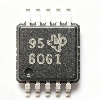
ADC084S101CIMMX - 4-Ch 8-Bit 1 Msps ADC | Texas Instruments
N.º da peça: ADC084S101CIMMX ✓ Ativo| Qtd. | Preço unitário | Total |
|---|---|---|
| 1 | $2.85 | $2,85 |
| 10 | $2.56 | $25,60 |
| 100 | $2.28 | $228,00 |
| 500 | $2.03 | $1.015,00 |
| 1.000 | $1.81 | $1.810,00 |
| 2.500 | $1.62 | $4.050,00 |
ADC084S101CIMMX Visão geral
An analog-to-digital converter (ADC) is a data-conversion integrated circuit that translates real-world analog signals into discrete digital codes for processing by microcontrollers, DSPs, or FPGAs. Within the broader taxonomy, an 8-bit SAR ADC sits between general-purpose ADCs (8 to 12 bits) and high-resolution ADCs (16 to 24 bits), occupying the speed-resolution sweet spot favored by instrumentation, motor control, and consumer designs. The ADC084S101CIMMX occupies the high-throughput end of this segment with throughput up to 1 Msps while maintaining low power consumption and a compact 10-pin VSSOP footprint suitable for space-constrained designs.
Key features include four single-ended input channels multiplexed into a single SAR core, straight-binary output serial data compatible with SPI, QSPI, MICROWIRE and common DSP serial interfaces, and individual channel shutdown capability via the CS input. The internal reference (typically 2.0 V) provides ratiometric conversion accuracy, with the analog input range extending from 0 V to VDD when using a 5 V supply. The serial data interface reduces board-routing complexity and pin count compared to parallel-output ADCs of similar performance, which is essential for compact PCB layouts.
Typical applications span industrial process control, multi-zone temperature monitoring, motor-current sensing, instrumentation digitizers, and portable battery-powered data acquisition where the low-power CMOS process and serial interface minimize both energy and board-area budgets. When designing with this part, ensure that the analog input does not exceed VDD or go below ground; bypass VDD with a 1 uF ceramic capacitor placed close to the supply pin and keep digital SCLK/CS/SDOUT traces short or impedance-controlled.
This page synthesizes distributor stock and pricing across multiple authorized channels, drop-in compatible VSSOP-10 alternatives, and practical design notes not found in the manufacturer datasheet.
Alternativas drop-in para ADC084S101CIMMX — mesmo encapsulamento, compatível pino a pino. Peças de encapsulamento diferente que exigem retrabalho na PCB são excluídas.
Variantes desta série
Modelos da mesma série compatíveis como drop-in com ADC084S101CIMMX (mesmo formato e footprint) — diferindo em Package, Operating Temperature, Digital Interface, Number of Input Channels, Resolution.
Ferramenta de comparação rápida — selecione peças alternativas para comparação lado a lado:
ADC084S101CIMM/NOPB
✅ Drop-In📋 Alternativa de referência (fora do catálogo)
ADC084S021CIMMX
✅ Drop-In✓ Em estoque
$1.6 / unidade
Ver ficha técnica →ADC104S101CIMM/NOPB
✅ Drop-In📋 Alternativa de referência (fora do catálogo)
ADC124S101CIMM/NOPB
✅ Drop-In📋 Alternativa de referência (fora do catálogo)
ADC08832IWM/NOPB
✅ Drop-In ⚠️ Especificações não verificadas✓ Em estoque
$1.92 / unidade
Ver ficha técnica →AD7918BRUZ
✅ Drop-In ⚠️ Especificações não verificadas📋 Alternativa de referência (fora do catálogo)
ADC084S101CIMMX Classificações máximas e características elétricas
| Nenhuma especificação disponível |
Configuração de pinos do ADC084S101CIMMX
| Pino 1 | VDD — Positive supply voltage input (2.7 V to 5.25 V) |
| Pino 2 | IN0 — Analog input channel 0 (single-ended) |
| Pino 3 | IN1 — Analog input channel 1 (single-ended) |
| Pino 4 | IN2 — Analog input channel 2 (single-ended) |
| Pino 5 | IN3 — Analog input channel 3 (single-ended) |
| Pino 6 | GND — Analog and digital ground |
| Pino 7 | CS — Chip-select input (active-low, also used for shutdown control) |
| Pino 8 | DOUT — Serial data output - SPI/QSPI/MICROWIRE-compatible |
| Pino 9 | SCLK — Serial clock input - drives SAR conversion and shifts data out |
| Pino 10 | REF — Reference-related pin (internal 2.0 V reference / bypass per datasheet) |
Aplicações típicas
ADC084S101CIMMX é adequado para 6 aplicaçãos: Industrial Process Control and Multi-Channel Monitoring, Battery-Powered Sensor Data Acquisition, Motor Current and Position Feedback Loops, Portable Instrumentation and Handheld Meters, LED Driver Backlight and Display Dimming Control, Consumer Audio Visual Switchers.
Industrial Process Control and Multi-Channel Monitoring
The ADC084S101CIMMX fits industrial process-control digitizers because of its four single-ended input channels mux'd into one SAR core, throughput up to 1 Msps, and 3.6 mW dissipation at 500 ksps/3 V. The internal 2.0 V reference eliminates an external precision reference. Designers typically place the part on a 4-20 mA loop-conditioned analog front-end and stream SPI data to a microcontroller for closed-loop control; the wide 2.7 V to 5.25 V supply range supports both 3.3 V and 5 V MCUs. Trade-off: 8-bit resolution suits setpoint monitoring but not precision measurement - choose ADC124S101 for 12-bit needs.
Recomendado
Battery-Powered Sensor Data Acquisition
The ADC084S101CIMMX is well-suited to battery-powered sensor DAQ where each milliamp matters: at 500 ksps and 3 V supply it draws only 3.6 mW, and the SAR architecture with SCLK-driven conversions means the part can be fully power-cycled between conversions via the CS pin, dropping quiescent current dramatically. With a single +2.7 V to +5.25 V supply and no external reference needed, total BOM cost and PCB area stay low. Use the part with a 1 uF VDD bypass capacitor and short analog traces; for ultra-low-power designs (sleep current dominated), drop to the ADC084S021CIMMX at 50-200 ksps.
Recomendado
Motor Current and Position Feedback Loops
The ADC084S101CIMMX fits high-speed motor feedback loops thanks to its 500 ksps to 1 Msps throughput - sufficient to digitize current-sense amplifier outputs at 20 kHz PWM rates with 5 to 10x oversampling. The 4 input channels let one ADC digitize three phase currents plus DC-bus voltage in a 3-phase BLDC/PMSM drive, while the SAR architecture guarantees no analog latency between conversions. Place the part near the sense resistors, route SCLK/CS/SDOUT to a DSP or MCU, and use VDD as the analog reference (ratiometric) for first-cut motor control designs.
Recomendado
Portable Instrumentation and Handheld Meters
The ADC084S101CIMMX is well-matched to portable meters because of its compact VSSOP-10 footprint, low 3.6 mW dissipation, and wide 2.7 V to 5.25 V supply range that accepts common battery chemistries (2xAA/AAA or Li-Ion). The internal 2.0 V reference removes an expensive external reference from the BOM. Typical designs mux thermocouple/strain-gauge/pressure inputs into the four channels; designers add low-noise op-amps between sensor and ADC inputs. Trade-off: 8-bit resolution is fine for display-grade meters but not for precision instrumentation - step up to ADC124S101 for 12-bit.
Recomendado
LED Driver Backlight and Display Dimming Control
The ADC084S101CIMMX suits LED backlight digitizers that need a fast feedback channel for ambient-light sensor and current-sense amplifier monitoring. Its 1 Msps sampling supports multi-channel dimming loops for RGB or area-lit panels at PWM rates up to several kHz, while 8-bit resolution is sufficient for backlight and ambient-light digitization. The SAR conversion is deterministic so backlight control loops remain stable. Place a ferrite bead on VDD to isolate the ADC from noisy LED driver rails, and route the four analog inputs directly from the four selected current-sense amplifiers.
Recomendado
Consumer Audio Visual Switchers
The ADC084S101CIMMX is well-suited to consumer AV switchers that need to monitor multiple analog signal levels for auto-gain, mute detection, or level-meter display. Its 4 channels fit a typical 4-input HDMI/analog switch with one spare for supply monitoring, and the 1 Msps throughput allows fast level-meter updates at display refresh rates. The compact VSSOP-10 footprint is friendly to cramped switcher housings. Use with 3.3 V supply rails common in modern consumer AV SoCs.
Recomendado
Resumo dos produtos recomendados
Dados de referência de engenharia para ADC084S101CIMMX — comparação, orientação de projeto e informações de conformidade.
Guia de seleção
Comparação com alternativas
| Parâmetro | Este produto | ADC084S101CIMM/NOPB | ADC084S021CIMMX | ADC104S101CIMM/NOPB | ADC124S101CIMM/NOPB | AD7918BRUZ |
|---|---|---|---|---|---|---|
| Package | VSSOP-10 | VSSOP-10 - same | VSSOP-10 - same | VSSOP-10 - same | VSSOP-10 - same | VSSOP-10 - same |
| Brand | Texas Instruments | Texas Instruments | Texas Instruments | Texas Instruments | Texas Instruments | Analog Devices |
| Resolution | 8 bits | 8 bits | 8 bits | 10 bits | 12 bits | 10 bits |
| Sample Rate | 500 ksps to 1 Msps | 500 ksps to 1 Msps | 50 ksps to 200 ksps | 500 ksps to 1 Msps | 500 ksps to 1 Msps | up to 1 Msps |
| Number of Channels | 4 | 4 | 4 | 4 | 4 | 1 |
| Supply Voltage | 2.7 V to 5.25 V | 2.7 V to 5.25 V | 2.7 V to 5.25 V | 2.7 V to 5.25 V | 2.7 V to 5.25 V | 2.7 V to 5.25 V |
| Internal Reference | 2.0 V | 2.0 V | 2.0 V | 2.0 V | 2.0 V | 2.5 V |
| Architecture | SAR | SAR | SAR | SAR | SAR | SAR |
| Digital Interface | SPI / QSPI / MICROWIRE | SPI / QSPI / MICROWIRE | SPI / QSPI / MICROWIRE | SPI / QSPI / MICROWIRE | SPI / QSPI / MICROWIRE | SPI/QSPI/MICROWIRE |
| Operating Temperature | -40C to +85C | -40C to +85C | -40C to +85C | -40C to +85C | -40C to +85C | -40C to +85C |
Principais diferenciais
- Lowest cost 4-channel 1 Msps 8-bit SAR ADC in TI portfolio (vs ADC104S101CIMM/NOPB)
- Wide supply range suits both 3.3 V and 5 V rails (vs ADC084S021CIMMX)
- Internal 2.0 V reference removes external reference from BOM (vs AD7918BRUZ)
Notas de projeto
The ADC084S101CIMMX draws approximately 3.6 mW at 500 ksps with a 3 V VDD. To stay within the rated supply ripple of 100 mV pk-pk, decouple VDD with a 1 uF X7R ceramic bypass capacitor placed within 3 mm of the pin and a 0.1 uF high-frequency bypass in parallel. For 5 V supplies the dissipation rises to about 7 mW at 500 ksps; at 1 Msps and 5 V it can reach 12 mW. Avoid series ferrite beads on VDD - use a low-ESR inductor or PCB trace plus bypass instead.
Route analog input traces IN0-IN3 as short 0.2 mm micro-strips with a continuous ground plane on layer 2, and add a 10-100 ohm source resistor to dampen any amplifier kickback into the input. Keep digital SCLK/CS/DOUT traces on the opposite side of the ground plane, length-matched if possible, and place the ADC084S101CIMMX at least 5 mm away from switch-mode power stages. If using an external reference override, route REF to a quiet region with its own bypass capacitor.
Three common pitfalls with the ADC084S101CIMMX: (1) forgetting that the analog input is single-ended with a 0V to VDD range - tying INx to a negative-rail sensor output will exceed the absolute-maximum rating; (2) leaving CS floating - CS MUST be driven low for any conversion to begin, so tie it to a GPIO or controlled signal, never leave it open; (3) attempting to read the part with software SPI at full 1 Msps when the host MCU cannot sustain that SCLK - verify timing budget on the master's master-clock rate before assuming throughput.
At 1 Msps the SCLK can run up to 20 MHz per the SPI mode-0 timing diagram. To avoid digital-coupling into the analog inputs, source-terminate SCLK with 33-ohm series resistors near the MCU driver, and add 4.7 kohm pull-ups on CS. SDOUT transitions on SCLK edges - if glitches couple into INx through the ground plane, increase the ground pour around the ADC by at least 50% and re-spin. Consider an RC low-pass (10 ohm + 100 pF) on the analog inputs if the upstream op-amp bandwidth exceeds the SCLK fifth harmonic.
Informações de conformidade
Pb-free / RoHS-compliant variant is the ADC084S101CIMM/NOPB; the plain ADC084S101CIMMX carrier may carry tin-lead plating per older datasheet revisions - check TI's lead-free/RoHS data sheet revision for confirmation. No AEC-Q100 grade (industrial grade only).