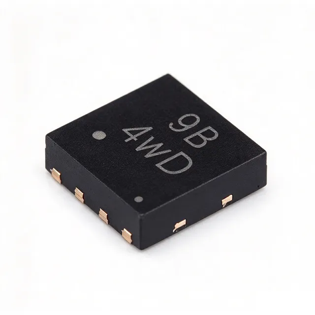
AP3441SHE-7B - 3A, 1MHz Sync Step-Down DC-DC Converter | Diodes
N.º da peça: AP3441SHE-7B ✓ Ativo| Qtd. | Preço unitário | Total |
|---|---|---|
| 1 | $1.5469 | $1,55 |
| 10 | $1.1172 | $11,17 |
| 100 | $0.9883 | $98,83 |
| 500 | $0.9453 | $472,65 |
| 1.000 | $0.9023 | $902,30 |
AP3441SHE-7B Visão geral
A buck (step-down) DC-DC converter is a switching regulator that efficiently reduces a higher DC input voltage to a lower DC output voltage by alternately storing energy in an inductor and releasing it into a load. Synchronous buck ICs integrate both the high-side and low-side MOSFETs, replacing the traditional rectifier diode with a low-Rds(on) MOSFET to achieve peak efficiencies above 90%. Within the broader taxonomy, AP3441 belongs to: switching regulator -> DC-DC converter -> power management IC -> semiconductor. It is purpose-built for low-voltage, high-current point-of-load (POL) conversion in portable and space-constrained products.
Key features of the AP3441SHE-7B include 55 µA typical no-load quiescent current, sub-1 µA shutdown current, internal soft-start, thermal shutdown, cycle-by-cycle current limit, and constant-frequency PWM control with no required external compensation components. The high 1 MHz switching frequency enables the use of small inductors and ceramic output capacitors, shrinking the total solution footprint to roughly the size of the IC package itself. At heavy loads, the PWM control provides excellent stability and fast transient recovery; at light loads the device automatically transitions to a pulse-frequency modulation (PFM) mode to sustain high efficiency.
The architecture uses a peak-current-mode control loop with internal slope compensation and an integrated synchronous MOSFET, allowing stable operation with ceramic output capacitors without ESR-related stability concerns. The exposed thermal pad on the underside of the UDFN-8 package provides a low thermal resistance path to PCB copper, sustaining the 3 A continuous output rating across the -40 °C to +85 °C operating range.
Typical applications include single-cell Li+/Li-polymer battery powered systems, USB-powered devices, solid-state drives (SSD), portable media players, point-of-load conversion for FPGAs, ASICs, and DSPs, and distributed 3.3 V/5 V bus regulation in networking and consumer products. The wide input range also makes it suitable for multi-cell alkaline or NiMH battery stacks as well as standard 3.3 V and 5 V rails.
When designing, select a 1 µH to 4.7 µH shielded inductor with a saturation rating above the peak inductor current (around 4 A for 3 A loads), place input/output ceramic capacitors as close as possible to the IC, and provide at least four thermal vias under the exposed pad to spread heat. To preserve efficiency, route the feedback trace away from the inductor and switching nodes. This page consolidates tier pricing, drop-in alternatives, and design notes that go beyond the datasheet to accelerate your design-in.
This page synthesizes distributor tier pricing, drop-in pin-compatible alternatives, and practical PCB-layout design notes not found in the manufacturer datasheet.
Alternativas drop-in para AP3441SHE-7B — mesmo encapsulamento, compatível pino a pino. Peças de encapsulamento diferente que exigem retrabalho na PCB são excluídas.
Ferramenta de comparação rápida — selecione peças alternativas para comparação lado a lado:
AP3441LSHE-7B
📋 Alternativa de referência (fora do catálogo)
AP3441SHE-7A
📋 Alternativa de referência (fora do catálogo)
AP3441SHE-7B Classificações máximas e características elétricas
| Topologia | Synchronous Buck (Step-Down) |
| Faixa de tensão de entrada | 2.7 V to 5.5 V |
| Faixa de tensão de saída | 0.6 V to VIN |
| Reference Voltage Accuracy | ±1.5% |
| Corrente máxima de saída | 3 A |
| Frequência de comutação | 1 MHz (typical) |
| Quiescent Current (No Load) | 55 µA (typical) |
| Corrente de desligamento | <1 µA |
| Duty Cycle | 100% (low-dropout operation) |
| Control Method | Constant-frequency PWM with PFM light-load |
| External Compensation | Not required |
| Retificador síncrono | Internal MOSFET |
| Temperatura de operação | -40 °C to +85 °C (TA) |
| Encapsulamento | U-DFN2020-8 (UDFN-8) with EP |
| Tipo de montagem | Surface Mount |
| Status RoHS | Compliant |
Configuração de pinos do AP3441SHE-7B
| Pino 1 | EN — Enable input (active-high). Drive high to enable the device; drive low for shutdown (<1 µA). |
| Pino 2 | VIN — Input supply voltage (2.7 V to 5.5 V). Decouple with 22 µF ceramic capacitor as close as possible. |
| Pino 3 | GND — Power ground return for internal MOSFETs and control circuitry. |
| Pino 4 | LX — Switching node to the external inductor. Connect to a 1 µH-4.7 µH shielded inductor. |
| Pino 5 | FB — Feedback input for output voltage regulation. Connect to external resistor divider; VREF = 0.6 V. |
| Pino 6 | COMP — Compensation node for control loop stability (internal compensation - no external components required). |
| Pino 7 | PGND — Power ground for low-side synchronous MOSFET (tie to GND on PCB). |
| Pino 8 | PG — Power-good open-drain output. Pull-up to logic rail with external resistor; pulled low when output is out of regulation. |
Aplicações típicas
AP3441SHE-7B é adequado para 6 aplicaçãos: Single-Cell Li+/Li-Polymer Battery Power, USB-Powered 5 V Device Power Supply, Solid-State Drive (SSD) Point-of-Load, FPGA/ASIC Core and I/O Rail Generation, Portable Consumer Electronics, Distributed 5 V/3.3 V Bus Regulation.
Single-Cell Li+/Li-Polymer Battery Power
The AP3441SHE-7B's 2.7 V to 5.5 V input window aligns precisely with the discharge curve of a single Li+/Li-polymer cell (4.2 V fully charged down to ~3.0 V cutoff), so it can power the core rails of a handheld product directly from the battery without a pre-regulator. The 3 A continuous rating covers most application-processor and memory rails in tablets, e-cigarettes, and portable medical devices. With 55 µA quiescent current and <1 µA shutdown, the device preserves battery life in standby. The 1 MHz fixed frequency and 100% duty-cycle operation allow the output to track the battery all the way down to its cutoff without losing the output line. Use a 1 µH to 2.2 µH shielded inductor and 22 µF X5R ceramic input/output capacitors for a typical 1.2 V/3 A solution under 50 mm².
Recomendado
USB-Powered 5 V Device Power Supply
The AP3441SHE-7B accepts the standard 5 V USB rail directly and steps it down to common sub-core/voltage domains (3.3 V, 2.5 V, 1.8 V, 1.2 V, 1.0 V) required by USB peripherals, hubs, and Type-C devices. The synchronous rectifier and 1 MHz PWM deliver peak efficiency above 90%, which is critical for USB 2.0/3.0 devices that must stay under the 2.5 W/4.5 W port-power budget. The internal soft-start limits inrush during USB hot-plug events, and the <1 µA shutdown current lets the device meet USB suspend-current requirements. Pair it with the AP2141 USB power switch upstream to form a compliant, protected USB-powered buck supply.
Recomendado
Solid-State Drive (SSD) Point-of-Load
Inside a SATA or NVMe SSD, the AP3441SHE-7B converts the host-supplied 5 V (or 3.3 V) rail into the 1.2 V, 1.0 V, and 0.8 V core voltages required by the NAND flash array and the SSD controller ASIC. The 3 A continuous output handles peak write-current transients common in TLC/QLC NAND programming bursts. The constant-frequency PWM control provides excellent transient response, critical when the controller toggles between idle and high-current write states within microseconds. The U-DFN2020-8 footprint (2 mm × 2 mm) allows multiple buck rails to be placed adjacent to the controller on a dense, miniaturized PCB. Place four thermal vias under the EP pad to sustain 3 A continuous at the typical 70 °C SSD ambient.
Recomendado
FPGA/ASIC Core and I/O Rail Generation
Modern FPGAs and ASICs require multiple low-voltage, high-current rails (e.g., 1.0 V core, 1.8 V/2.5 V/3.3 V I/O) generated from a 3.3 V or 5 V system bus. The AP3441SHE-7B's 3 A output and 1 MHz switching frequency make it an excellent point-of-load (POL) converter for these rails, especially in cost-sensitive designs where a fully featured PMIC is overkill. The 0.6 V reference accuracy of ±1.5% keeps the FPGA core rail within its tolerance window, and the fast PWM transient response handles current steps during logic-block wake-up events. Multiple AP3441SHE-7B devices can be paralleled on different rails on the same board, all switching in-phase to simplify EMI filtering.
Recomendado
Portable Consumer Electronics
The AP3441SHE-7B's 1 MHz fixed frequency, sub-50 mm² solution size, and 3 A output make it ideal for portable media players, wireless headphones, handheld game consoles, and digital camcorders. These products demand long battery life, low standby drain, and a small PCB footprint - all met by the device's 55 µA quiescent current, <1 µA shutdown, and tiny U-DFN2020-8 package. The wide 2.7-5.5 V range accepts direct connection to a single Li-ion cell, USB input, or a boost converter output. The integrated synchronous MOSFET eliminates an external Schottky diode, reducing BOM cost and shrinking the layout.
Recomendado
Distributed 5 V/3.3 V Bus Regulation
On a 3.3 V or 5 V distributed power bus (common in industrial controllers, networking switches, and test equipment), the AP3441SHE-7B steps the bus down to sub-volt rails for local loads such as sensors, ADC/DAC references, and interface ICs. Placing a buck at each load point improves transient response and reduces distribution losses versus running multiple lower-current rails directly from the main converter. The device's 3 A capability covers most mixed-signal load clusters on a single board, and the small U-DFN2020-8 package allows placement adjacent to the load. Use the 100% duty-cycle feature to maintain regulation when the input bus sags under heavy bus load.
Recomendado
Resumo dos produtos recomendados
Dados de referência de engenharia para AP3441SHE-7B — comparação, orientação de projeto e informações de conformidade.
Guia de seleção
Comparação com alternativas
| Parâmetro | Este produto | AP3441LSHE-7B | AP3441SHE-7A |
|---|---|---|---|
| Package | U-DFN2020-8 | U-DFN2020-8 - same | U-DFN2020-8 - same |
| Brand | Diodes Incorporated | Diodes Incorporated | Diodes Incorporated |
| Input Voltage Range | 2.7 V to 5.5 V | 2.7 V to 5.5 V | 2.7 V to 5.5 V |
| Output Current | 3 A | 3 A | 3 A |
| Switching Frequency | 1 MHz | 1 MHz | 1 MHz |
| Output Voltage Range | 0.6 V to VIN | 0.6 V to VIN | 0.6 V to VIN |
| Quiescent Current | 55 µA | 55 µA | 55 µA |
| Synchronous Rectifier | Internal MOSFET | Internal MOSFET | Internal MOSFET |
| External Compensation | Not required | Not required | Not required |
| Duty Cycle | 100% (LDO mode) | 100% (LDO mode) | 100% (LDO mode) |
Principais diferenciais
- Same U-DFN2020-8 package as AP3441LSHE-7B with full electrical compatibility (vs AP3441LSHE-7B)
- Higher output current than typical 8-pin DFN competitors (vs AP63205WU-7)
- No external compensation components required (vs TPS54302DDC (TI))
Notas de projeto
Place the input capacitor (22 µF X5R ceramic, 10 V rating) as close as possible to the VIN and GND pins (pins 2 and 3), with the ground side returning directly to the IC ground. Place the bootstrap/feedback capacitor (if any) close to its respective pin. Keep the LX trace short and wide to minimize parasitic inductance and EMI radiation. Per the AP3441 datasheet typical application circuit, the inductor should be placed adjacent to the LX pin with the output ceramic capacitor returning to PGND. Estimated: with 1 oz copper and 4 thermal vias under the exposed pad, thermal resistance is roughly 50 °C/W, allowing ~2 W dissipation at 85 °C ambient before derating.
At 3 A load with VIN = 5 V and VOUT = 3.3 V, power dissipation is (5 - 3.3) × 3 × (1 - η) where efficiency η is around 92%, so dissipation is roughly 0.4 W. The U-DFN2020-8 package has theta_JA of approximately 50 °C/W on a 4-layer 1 oz board with thermal vias, giving a junction rise of 20 °C above ambient. At higher VIN-VOUT differentials (5 V to 1 V, 3 A) dissipation rises to ~1.5 W; the exposed pad MUST have at least 4 thermal vias to the inner ground plane for reliable operation. Estimated: thermal pad via count and copper area dominate thermals - keep top-layer copper pour over the EP unbroken.
Do not operate the AP3441SHE-7B above 5.5 V input - absolute maximum is 6 V, and sustained overvoltage will trigger the internal OVP/clamp and may damage the device. Do not omit the input ceramic capacitor; the synchronous rectifier's high-side MOSFET needs a low-inductance input source to prevent voltage spikes on VIN. Avoid routing the FB trace near the inductor or LX node - capacitive coupling introduces switching noise into the feedback loop and degrades load regulation. Finally, ensure the EN pin is driven from a clean logic source; if driven by a high-impedance node, add a 100 kΩ pull-down to keep the device off during power-up sequencing.
Informações de conformidade
RoHS compliant per Diodes Incorporated product page. Not AEC-Q100 qualified - this is a commercial/industrial grade part. Halogen-free status not explicitly stated in the verified data - confirm with the manufacturer datasheet before use in halogen-free PCB assemblies.




