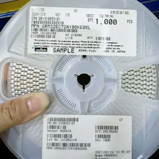
GRM0335C1E101JA01D - 100pF 25V C0G 0201 MLCC | Murata
N.º da peça: GRM0335C1E101JA01D ✓ Ativo| Qtd. | Preço unitário | Total |
|---|---|---|
| 1 | $0.01 | $0,01 |
| 10 | $0.01 | $0,10 |
| 100 | $0.01 | $1,00 |
| 500 | $0.01 | $5,00 |
| 1.000 | $0.01 | $10,00 |
GRM0335C1E101JA01D Visão geral
An MLCC (multilayer ceramic capacitor) is a passive component that stores charge in alternating layers of ceramic dielectric and metal electrodes. Within the capacitor hierarchy, it sits under ceramic capacitors, which sit under fixed capacitors, and it is one of the most widely deployed passives in modern electronics. Temperature-compensating Class 1 dielectrics such as C0G (also written NP0, meaning negative-positive zero) exhibit a temperature coefficient of 0 ±30 ppm/degC, making them the most stable ceramic capacitor class available.
Key features of the GRM0335C1E101JA01D include a tight ±5% (J code) capacitance tolerance, a wide operating temperature range of -55degC to +125degC, and the drift-free C0G dielectric that exhibits negligible capacitance change with voltage, temperature, and aging. Unlike Class 2 dielectrics (X7R, X5R), C0G parts do not lose capacitance under DC bias and have very low dissipation factor, which suits resonant and timing circuits.
Technically, the C0G dielectric is formed from paraelectric ceramic materials, giving near-linear behavior and low loss at high frequencies. The 0201 case supports high-density assembly with 0.2 mm minimum distance between external terminals and 0.1 to 0.2 mm external terminal width, enabling fine-pitch land patterns in smartphones, wearables, and RF modules. The part is supplied on tape and reel for automated pick-and-place.
Typical applications include RF matching networks and filters, crystal oscillator load capacitance, precision analog timing circuits, and high-frequency decoupling where capacitance stability directly affects circuit accuracy.
A key design consideration is that the 25 VDC rating must be derated appropriately; although C0G shows minimal DC bias effect, transient overvoltage and flex cracking remain risks in thin 0201 packages, so careful PCB lands are advised.
This page synthesizes distributor availability data, drop-in alternative options, and practical design notes not consolidated in the manufacturer datasheet.
Alternativas drop-in para GRM0335C1E101JA01D — mesmo encapsulamento, compatível pino a pino. Peças de encapsulamento diferente que exigem retrabalho na PCB são excluídas.
Ferramenta de comparação rápida — selecione peças alternativas para comparação lado a lado:
GRM0335C1E101JD01D
✅ Drop-In📋 Alternativa de referência (fora do catálogo)
GRM0335C1E101JA01J
✅ Drop-In ⚠️ Especificações não verificadas📋 Alternativa de referência (fora do catálogo)
GRM0335C1E101JA01W
✅ Drop-In ⚠️ Especificações não verificadas📋 Alternativa de referência (fora do catálogo)
GRM0335C1E101JA01D Classificações máximas e características elétricas
| Capacitance | 100 pF |
| Capacitance Tolerance | ±5% (J code) |
| Rated Voltage | 25 VDC |
| Dielectric | C0G (NP0) |
| Temperature Coefficient | 0 ±30 ppm/degC |
| Faixa de temperatura de operação | -55degC to +125degC |
| Case Size (inch/metric) | 0201 (0603 metric) |
| Case Length | 0.6 ±0.03 mm |
| Case Width | 0.3 ±0.03 mm |
| Case Thickness | 0.3 ±0.03 mm |
| Distance Between External Terminals (g) | 0.2 mm min. |
| External Terminal Size (e) | 0.1 to 0.2 mm |
| Series | GRM |
| Tipo de montagem | Surface Mount (SMD/SMT) |
| Packaging | Tape & Reel |
Guia de Configuração de Pinos do GRM0335C1E101JA01D 0.3 ±0.03 mm
Configuração de pinos para GRM0335C1E101JA01D (pacote 0.3 ±0.03 mm). A numeração dos pinos, funções e diagramas de conexão estão definidos no datasheet do fabricante. Consulte-o para o footprint exato e diretrizes de soldagem.

Nenhum dado detalhado de pinagem disponível para GRM0335C1E101JA01D.
Consulte a ficha técnica para a configuração completa dos pinos.
Aplicações típicas
GRM0335C1E101JA01D é adequado para 6 aplicaçãos: RF Matching Networks and Filters, Crystal Oscillator Load Capacitance, Precision Analog Timing and RC Circuits, High-Frequency Decoupling in Digital Designs, Smartphones, Wearables and IoT Modules, Automotive and Industrial Signal Conditioning.
RF Matching Networks and Filters
The GRM0335C1E101JA01D's C0G (NP0) dielectric provides 0 ±30 ppm/degC drift and very low loss, which keeps RF impedance match points stable across the -55degC to +125degC range. In 0201 (0603 metric) form, its tiny 0.6 x 0.3 x 0.3 mm body contributes minimal parasitic inductance, making it ideal for shunt or series elements in 50-ohm matching networks, LNA input filters, and antenna tuning circuits up to the multi-GHz range. Placed in a pi-network or lumped-element filter, the stable 100 pF ±5% value preserves the designed cutoff and notch frequencies over temperature and DC bias, unlike Class 2 dielectrics that shift with bias. Verify the self-resonant frequency against your band using the Murata S-parameter data.
Recomendado
Crystal Oscillator Load Capacitance
Crystal oscillators demand load capacitors whose value does not drift, because a 1 pF error can shift frequency by several ppm. The GRM0335C1E101JA01D's C0G dielectric holds 100 pF within ±5% with 0 ±30 ppm/degC temperature coefficient, and C0G exhibits virtually no DC bias or aging effect, keeping the effective load constant across the rated -55degC to +125degC range. Two of these capacitors can be placed from the crystal pins to ground, or combined in series pairs, to realize typical 12.5 pF to 20 pF load points precisely. The 25 VDC rating comfortably covers oscillator drive levels, and the 0201 case allows placement directly adjacent to the crystal pads for minimal stray inductance.
Recomendado
Precision Analog Timing and RC Circuits
RC timers, integrators, and sample-hold circuits rely on capacitance accuracy over time and temperature. The GRM0335C1E101JA01D combines a tight ±5% tolerance with the drift-free C0G (NP0) dielectric, so a 100 pF timing capacitor does not change value with applied voltage, temperature swings from -55degC to +125degC, or aging - failure modes common to X7R and X5R Class 2 MLCCs. In a precision monostable, relaxation oscillator, or switched-capacitor filter, this translates directly to timing accuracy and low dielectric absorption effects. The 0201 package supports dense mixed-signal layouts near precision op-amps and ADCs, keeping charge-injection nodes compact and symmetrical.
Recomendado
High-Frequency Decoupling in Digital Designs
C0G's low dissipation factor and low ESR make the GRM0335C1E101JA01D effective as a high-frequency decoupling element where a stable, low-loss 100 pF is needed close to IC power pins. In the 0201 case, its low parasitic inductance keeps the impedance minimum at high frequency, complementing larger bulk X7R capacitors that handle lower-frequency ripple. Typical placement is one 100 pF C0G per IC supply pin pair in MCUs, PHYs, and RF transceiver modules, positioned within 1 to 2 mm of the pin with short vias to the plane. Because C0G capacitance does not droop under DC bias, the actual decoupling value matches the schematic value at the full 25 VDC rating.
Recomendado
Smartphones, Wearables and IoT Modules
The 0201 (0603 metric) footprint of the GRM0335C1E101JA01D - just 0.6 x 0.3 x 0.3 mm with 0.2 mm minimum terminal spacing - is designed for ultra-high-density assemblies where board area is the binding constraint. In smartphone RF front ends, wearable sensor hubs, and IoT radio modules, thousands of passives must fit under a shield can, and 0201 C0G parts provide stable RF and timing capacitance in the smallest industry-standard case. The wide -55degC to +125degC operating range covers both outdoor and near-antenna thermal environments, and tape-and-reel packaging supports high-speed placement with standard 0201 nozzles and vision recognition.
Recomendado
Automotive and Industrial Signal Conditioning
The -55degC to +125degC operating range and stable C0G dielectric let the GRM0335C1E101JA01D serve in automotive sensor interfaces and industrial signal conditioning where capacitors sit near heat sources or in cold environments. Typical uses include anti-aliasing filters ahead of ADCs, snubber and resonant elements in sensing bridges, and filter capacitors in CAN and sensor supply lines where Class 2 dielectric drift would corrupt measurements. The 25 VDC rating provides margin on 12 V and 24 V-derived rails when used with appropriate series impedance. Confirm AEC qualification status against Murata's automotive series documentation before use in safety-related positions.
Recomendado
Resumo dos produtos recomendados
Dados de referência de engenharia para GRM0335C1E101JA01D — comparação, orientação de projeto e informações de conformidade.
Guia de seleção
Comparação com alternativas
| Parâmetro | Este produto | GRM0335C1E101JD01D | GRM0335C1E101JA01J | GRM0335C1E101JA01W |
|---|---|---|---|---|
| Package | 0201 (0603 Metric) | 0201 (0603 Metric) - same | 0201 (0603 Metric) - same | 0201 (0603 Metric) - same |
| Brand | Murata Manufacturing | Murata Manufacturing | Murata Manufacturing | Murata Manufacturing |
| Capacitance | 100 pF | 100 pF | 100 pF | 100 pF |
| Tolerance | ±5% (J) | ±5% (J) | ±5% (J) | ±5% (J) |
| Rated Voltage | 25 VDC | 25 VDC | 25 VDC | 25 VDC |
| Operating Temperature | -55degC to +125degC | -55degC to +125degC | -55degC to +125degC | -55degC to +125degC |
| Case Dimensions | 0.6 x 0.3 x 0.3 mm | 0.6 x 0.3 x 0.3 mm | 0.6 x 0.3 x 0.3 mm | 0.6 x 0.3 x 0.3 mm |
| Primary Distinction | Baseline C0G 0201 100 pF 25 V part | Different temperature-characteristic code | Alternate packing suffix (same family) | Alternate packing suffix (same family) |
Principais diferenciais
- Temperature-compensating C0G dielectric with 0 ±30 ppm/degC drift (vs GRM0335C1E101JD01D)
- Tight ±5% (J) tolerance in a 0201 case (vs Generic 0201 C0G parts with ±10% (K) tolerance)
- Trade-off: small capacitance value and 25 V limit (vs GRM0335C1E101JD01D and larger-case C0G siblings)
Notas de projeto
For the 0201 case, use a land pattern matched to the 0.6 x 0.3 x 0.3 mm body with 0.2 mm minimum internal terminal spacing per the Murata datasheet. Avoid oversized pads: excess solder fillet increases flex-crack risk and raises parasitic capacitance in RF layouts. Follow IPC-recommended 0201 land dimensions, use solder mask defined or non-solder-mask defined pads consistently, and verify stencil aperture design (typically laser-cut, 75-100 um) to prevent mid-chip or tombstone defects during reflow.
Do not exceed the 25 VDC rated voltage; check transient spikes on switched rails, not just nominal levels. Although C0G capacitance is essentially bias-independent, mechanical board flex during depaneling, connector insertion, or thermal cycling can crack 0201 ceramics - orient capacitors perpendicular to board flex direction and keep them away from mounting holes and V-score edges. Never substitute a Class 2 (X7R) part in timing or RF positions without re-verifying the DC bias characteristic.
In RF paths, the effective capacitance includes pad and trace parasitics; a 0201 C0G placed on typical FR-4 pads adds roughly 0.05-0.15 pF of parasitic depending on stackup. For matching networks, simulate with the Murata S-parameter or library file for GRM0335C1E101JA01D rather than the ideal 100 pF value. Place series elements in the trace and shunt elements with the shortest possible ground vias; keep ground return paths continuous beneath RF capacitors.
Informações de conformidade
Distributor listings (DigiKey, Mouser, Newark, TTI) identify this Murata GRM series MLCC as RoHS-compliant, lead-free surface mount. Formal REACH and halogen-free declarations should be confirmed via the official Murata product page and material declaration sheets.