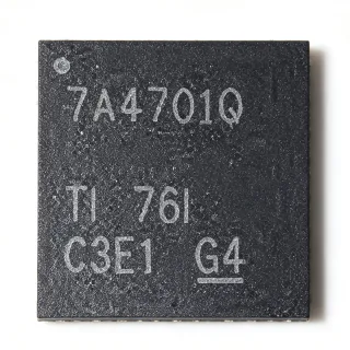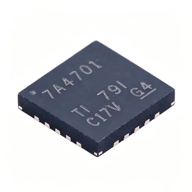
TPS7A4701RGWR - 1A, 36V Ultra-Low Noise LDO | Texas Instruments
N.º da peça: TPS7A4701RGWR ✓ Ativo| Qtd. | Preço unitário | Total |
|---|---|---|
| 1 | $3.25 | $3,25 |
| 10 | $2.95 | $29,50 |
| 100 | $2.6 | $260,00 |
| 500 | $2.35 | $1.175,00 |
| 1.000 | $2.1 | $2.100,00 |
TPS7A4701RGWR Visão geral
An LDO (low-dropout) linear regulator is a type of voltage regulator that maintains a stable output voltage even when the input voltage is only marginally higher than the output. Within the power management IC hierarchy, LDOs sit downstream of switching converters, providing the final, noise-free regulation stage that sensitive analog loads require. Unlike DC-DC converters, LDOs add no switching ripple, which is why they dominate RF, audio, and precision instrumentation power rails.
Key features include 4.17 uVRMS output noise over the 20 Hz to 100 kHz bandwidth, 1 A output capability, and a low dropout voltage of approximately 307 mV, per the TI TPS7A47 datasheet. The TPS7A4701 variant offers an externally adjustable output via a feedback pin, while the sibling TPS7A4700 uses a PCB-programmable scheme requiring no external resistors. An enable pin supports power sequencing in multi-rail systems.
The device is built on bipolar technology, chosen specifically for high-accuracy, high-precision instrumentation where clean rails maximize system performance. According to TI, the TPS7A47 family is optimized for powering operational amplifiers, ADCs, DACs, and other high-performance analog circuitry, where its high power-supply rejection suppresses upstream switching-converter ripple.
Typical applications include RF PLL/VCO power supplies in transceivers, audio DAC/ADC analog rails, precision test-and-measurement instrumentation, and industrial systems running from 24 V buses where the 36 V input rating provides ample headroom.
A key design consideration is thermal budget: at large input-to-output differentials and full 1 A load, dissipation can reach several watts, so the exposed pad must be soldered to a generous copper pour. The NR/SS capacitor also sets soft-start and noise-reduction bandwidth and should not be omitted.
This page synthesizes distributor pricing (as of 2026-09-01), drop-in alternatives, and practical design notes not found in the manufacturer datasheet.
Alternativas drop-in para TPS7A4701RGWR — mesmo encapsulamento, compatível pino a pino. Peças de encapsulamento diferente que exigem retrabalho na PCB são excluídas.
Variantes desta série
Modelos da mesma série compatíveis como drop-in com TPS7A4701RGWR (mesmo formato e footprint) — diferindo em Output Noise, Output Type, Output Voltage Range, Enable Pin, Input Voltage Range.
Ferramenta de comparação rápida — selecione peças alternativas para comparação lado a lado:
TPS7A4700RGWR
✅ Drop-In✓ Em estoque
$3.6591 / unidade
Ver ficha técnica →TPS7A4701QRGWRQ1
✅ Drop-In✓ Em estoque
$3.48 / unidade
Ver ficha técnica →TPS7A3301RGWR
✅ Drop-In📋 Alternativa de referência (fora do catálogo)
TPS7A4701RGWR Classificações máximas e características elétricas
| Tipo de saída | Positive Adjustable, 1 channel |
| Faixa de tensão de saída | 1.4 V to 34 V |
| Corrente máxima de saída | 1 A |
| Faixa de tensão de entrada | 3 V to 36 V |
| Tensão de dropout | 307 mV |
| Ruído de saída | 4.17 uVRMS |
| Technology | Bipolar |
| Encapsulamento | 20-VQFN (5x5 mm) with exposed pad |
| Tipo de montagem | Surface Mount |
| Pino de habilitação | Yes |
| Product Family | TPS7A47 RF LDO |
| Marking Code | 7A4701 |
| Packaging | Tape & Reel (T/R) |
Guia de Configuração de Pinos do TPS7A4701RGWR 20-vqfn (5x5 mm) with exposed pad
Configuração de pinos para TPS7A4701RGWR (pacote 20-vqfn (5x5 mm) with exposed pad). Este dispositivo de potência possui terminais de gate, drain e source. Para pacotes não polarizados, consulte o datasheet do fabricante para a orientação exata do pino 1 e detalhes do footprint. Aplicações comuns incluem projeto de fontes de alimentação, acionamento de motores e comutação de cargas.

Nenhum dado detalhado de pinagem disponível para TPS7A4701RGWR.
Consulte a ficha técnica para a configuração completa dos pinos.
Aplicações típicas
TPS7A4701RGWR é adequado para 6 aplicaçãos: RF PLL/VCO Power Supply, Precision Test and Measurement Instrumentation, High-End Audio DAC and ADC Supplies, Industrial 24V Bus Regulation, Precision ADC/DAC Reference Buffering Chains, Multi-Rail Processor and FPGA Analog Rails.
RF PLL/VCO Power Supply
RF synthesizers place extreme demands on supply noise: VCO pushing figures mean that even microvolts of rail noise convert directly into phase noise, degrading integrated jitter and EVM. The TPS7A4701RGWR addresses this with 4.17 uVRMS output noise (20 Hz to 100 kHz) and TI-classified RF LDO performance built on bipolar technology. It is typically placed after a switching pre-regulator, where its ripple rejection cleans the 5 V or 3.3 V rail feeding the PLL charge pump and VCO tuning supply. Because the part tolerates up to 36 V input, it can also regulate directly from higher intermediate rails. Designers should keep the NR/SS capacitor close to the pin to preserve the low-noise bandwidth and route the VCO supply as a star branch off the LDO output.
Recomendado
Precision Test and Measurement Instrumentation
Bench instruments, digitizers, and calibration hardware require analog rails with negligible noise so that the instrument itself does not become the dominant error source. According to TI, the TPS7A47 family is designed with bipolar technology primarily for high-accuracy, high-precision instrumentation where clean voltage rails maximize system performance. The TPS7A4701RGWR supplies op-amp and ADC stages from its 1.4 V to 34 V adjustable output, sourcing up to 1 A for multi-channel analog front ends. Its 36 V maximum input supports direct regulation from industrial supplies used in rack equipment. Thermal design matters: the exposed VQFN-20 pad must bond to a solid ground pour, and at large VIN-VOUT differentials the dissipation budget should be verified before layout release.
Recomendado
High-End Audio DAC and ADC Supplies
Audio DAC and ADC analog supplies directly influence dynamic range and THD+N; ripple or noise on AVDD appears as spurious tones in the output spectrum. The TPS7A4701RGWR's 4.17 uVRMS noise floor and bipolar architecture make it well suited to powering DAC analog rails and op-amp I/V conversion stages. Placed between a 12 V or 15 V supply and the DAC AVDD pin with 10 uF local ceramics, it adds no switching artifacts. The 1 A rating covers high-current DACs and their analog output stages. Compared with generic LDOs, the key benefit is noise floor; the trade-off is higher quiescent dissipation at large input-output deltas, so headroom should be minimized while maintaining the ~307 mV dropout margin.
Recomendado
Industrial 24V Bus Regulation
Industrial control and sensor-excitation systems commonly run from 24 V buses with transient excursions toward 30 V or more. The TPS7A4701RGWR's 3 V to 36 V input range provides direct headroom for these rails, eliminating an intermediate switching stage when load currents are moderate. It can generate clean 5 V or adjustable analog rails for transmitters, ADC front ends, and reference circuits on PLC I/O cards. Because dropout is approximately 307 mV at load, the part also works in post-regulation roles after a buck converter reduces the bus. Designers must account for worst-case dissipation at full differential - at 24 V input and 5 V output the device dissipates heavily at 1 A, so copper area or derating is essential.
Recomendado
Precision ADC/DAC Reference Buffering Chains
High-resolution converters are only as good as their supplies and references: PSR of an ADC falls with frequency, so high-frequency supply ripple leaks into conversion results. The TPS7A4701RGWR provides a quiet rail for the reference buffer amplifier and analog supply pins of 18- to 24-bit converters, with the 4.17 uVRMS noise figure translating into a sub-LSB noise contribution at typical reference levels. The adjustable output via the FB pin lets designers tune the rail to exactly the converter's recommended AVDD. Layout discipline - short, wide output traces and local 10 uF plus 0.1 uF decoupling - preserves the datasheet noise performance in the final assembly.
Recomendado
Multi-Rail Processor and FPGA Analog Rails
FPGAs and SoCs mix noisy core rails with noise-sensitive PLL, transceiver, and analog supplied rails. The TPS7A4701RGWR's enable pin supports sequenced power-up of the quiet rails after core supplies, satisfying FPGA power-supply sequencing requirements. Post-regulating a switching converter output down to the gigabit transceiver AVDD rail with this LDO suppresses switching residue and lowers jitter. The 1 A capability covers multiple transceiver banks, and the 36 V input allows the part to sit on unconditioned backplane supplies. Use the FB divider with 1%-tolerance resistors, and keep the soft-start NR/SS capacitor sized so inrush does not trip upstream protection.
Recomendado
Resumo dos produtos recomendados
Dados de referência de engenharia para TPS7A4701RGWR — comparação, orientação de projeto e informações de conformidade.
Guia de seleção
Comparação com alternativas
| Parâmetro | Este produto | TPS7A4700RGWR | TPS7A4701QRGWRQ1 | TPS7A3301RGWR |
|---|---|---|---|---|
| Package | 20-VQFN (5x5) exposed pad | 20-VQFN (5x5) - same | 20-VQFN (5x5) - same | 20-VQFN (5x5) - same |
| Brand | Texas Instruments | Texas Instruments | Texas Instruments | Texas Instruments |
| Output Current | 1 A | 1 A | 1 A | 1 A |
| Output Polarity / Range | Positive, 1.4 V to 34 V adjustable | Positive, PCB-programmed up to 20.5 V | Positive, 1.4 V to 34 V adjustable | Negative, -1.4 V to about -36 V |
| Automotive Qualification | No | No | Yes (Q1 variant) | No |
Principais diferenciais
- Resistor-adjustable output up to 34 V (vs TPS7A4700RGWR)
- 36 V input tolerance on a low-noise LDO (vs TPS7A8300RGRR)
- Standard (non-automotive) cost position (vs TPS7A4701QRGWRQ1)
Notas de projeto
Estimated: at VIN = 12 V, VOUT = 5 V, and full 1 A load, dissipation reaches about 7 W - far beyond what the VQFN-20 package can dissipate with a nominal footprint, so junction temperature will exceed limits without major copper area or airflow. For high-differential designs, either reduce load current, add a switching pre-regulator, or verify junction temperature using the theta-JA values in the TI datasheet for your specific PCB stackup. Solder the exposed thermal pad to a minimum 1-2 square inch solid ground pour with thermal vias.
Place a 10 uF ceramic input capacitor and 10 uF output capacitor within a few millimeters of the IN and OUT pins, and add a 0.1 uF capacitor in parallel on the output for high-frequency decoupling. The FB divider resistors should be 1% tolerance or better to preserve output accuracy, and their midpoint trace to the FB pin should be short and away from switching nodes. Keep the NR/SS capacitor loop tight - it sets the noise-reduction bandwidth that delivers the 4.17 uVRMS figure.
Do not exceed the 36 V absolute maximum input, and beware inductive spikes on long industrial wiring - input TVS protection is prudent on 24 V bus applications. Do not substitute the TPS7A3301 (negative LDO) for this part on positive rails despite the identical footprint. When replacing a TPS7A4700 with a TPS7A4701 on an existing PCB, the TPS7A4700's PCB-programmed output pattern must be disconnected and the FB network added; verify before reflow.
Use the enable pin for rail sequencing in multi-supply systems such as FPGA or ADC power trees, releasing the analog rail after the core supply is stable. The soft-start behavior governed by the NR/SS capacitor limits inrush into large output capacitor banks; size output capacitance accordingly to avoid tripping upstream current limits during startup.
Informações de conformidade
Standard TI catalog part, not marketed as AEC-Q100; the TPS7A4701QRGWRQ1 variant serves automotive requirements. RoHS/REACH certificates should be pulled from the TI product page for build documentation - values not present in the retrieved web data.