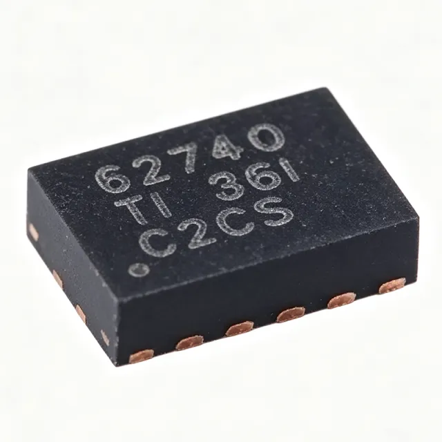
TPS62740DSSR - 300mA 360nA Iq Buck Converter | Texas Instruments
N.º da peça: TPS62740DSSR ✓ Ativo| Qtd. | Preço unitário | Total |
|---|---|---|
| 1 | $1.64 | $1,64 |
| 10 | $1.48 | $14,80 |
| 100 | $1.3 | $130,00 |
| 500 | $1.15 | $575,00 |
| 1.000 | $1.02 | $1.020,00 |
TPS62740DSSR Visão geral
A step-down (buck) converter is a switching voltage regulator that efficiently converts a higher input voltage to a lower output voltage using a switch, inductor, and capacitor. Within the power management IC hierarchy, it belongs to the DC-DC converter family, which achieves far higher efficiency than linear regulators by storing and transferring energy rather than dissipating it as heat. This makes buck converters the preferred choice for extending battery life in portable and IoT systems.
Key features include up to 90% efficiency at just 10uA output current, RF-friendly DCS-Control topology, and a switching frequency of up to 2MHz, which permits a tiny 2.2uH inductor and 10uF output capacitor for a total solution size of approximately 31mm2. The device also integrates a load switch, enabling system power gating of downstream circuitry to further reduce standby current.
The DCS-Control (Direct Control with Seamless Transition into Power Save Mode) architecture combines the low output ripple of PWM operation with the high light-load efficiency of PFM power-save mode, transitioning seamlessly without transient excursions. This is critical for RF power rails, where ripple and spurious noise can degrade transmitter phase noise and receiver sensitivity. Compared with conventional power-save-mode converters, the seamless transition means output impedance stays low across the entire load range, preserving output-voltage accuracy from full load down to nanoamp quiescent levels.
Typical applications include BLE beacons and sensors, energy harvesting systems, wearable devices, and battery-powered metering, where a single lithium or alkaline cell must power the system for months or years. With 360nA quiescent current, a coin cell (approx. 220mAh) can support a duty-cycled sensor node for several years in standby-dominated operation.
Design consideration: optimize the output capacitor ESR and inductor value per the TI datasheet recommendation (2.2uH, 10uF) to preserve the low-ripple, RF-friendly behavior in power-save mode.
This page synthesizes distributor pricing, drop-in alternatives, and practical design notes not found in the manufacturer datasheet.
Alternativas drop-in para TPS62740DSSR — mesmo encapsulamento, compatível pino a pino. Peças de encapsulamento diferente que exigem retrabalho na PCB são excluídas.
Ferramenta de comparação rápida — selecione peças alternativas para comparação lado a lado:
TPS62742DSSR
✅ Drop-In📋 Alternativa de referência (fora do catálogo)
TPS62741DSSR
✅ Drop-In ⚠️ Especificações não verificadas📋 Alternativa de referência (fora do catálogo)
TPS62740DSSR
✅ Drop-In✓ Em estoque
$1.02 / unidade
Ver ficha técnica →TPS62740DSSR Classificações máximas e características elétricas
| Topologia | Step-down (buck) DC-DC converter, DCS-Control |
| Faixa de tensão de entrada | 2.2 V to 5.5 V |
| Corrente máxima de saída | 300 mA |
| Corrente de repouso | 360 nA (typical) |
| Eficiência | Up to 90% at 10 uA output current |
| Frequência de comutação | Up to 2 MHz |
| Integrated Load Switch | Yes |
| Faixa de temperatura de operação | -40C to +85C |
| Encapsulamento | 12-WSON (DSS), 2x3 mm, exposed pad |
| Tipo de montagem | Surface Mount |
| Número de saídas | 1 |
| Control Architecture | DCS-Control with seamless transition into power save mode |
| Typical Inductor | 2.2 uH |
| Typical Output Capacitor | 10 uF |
| Application Segment | Bluetooth Low Energy (BLE), battery-powered wireless |
Guia de Configuração de Pinos do TPS62740DSSR 12-wson (dss), 2x3 mm, exposed pad
Configuração de pinos para TPS62740DSSR (pacote 12-wson (dss), 2x3 mm, exposed pad). Este dispositivo de potência possui terminais de gate, drain e source. Para pacotes não polarizados, consulte o datasheet do fabricante para a orientação exata do pino 1 e detalhes do footprint. Aplicações comuns incluem projeto de fontes de alimentação, acionamento de motores e comutação de cargas.

Nenhum dado detalhado de pinagem disponível para TPS62740DSSR.
Consulte a ficha técnica para a configuração completa dos pinos.
Aplicações típicas
TPS62740DSSR é adequado para 6 aplicaçãos: BLE Beacons and Sensors, Energy Harvesting Systems, Wearable Devices, Battery-Powered Metering, IoT Wireless Sensor Nodes, Portable Medical Monitoring.
BLE Beacons and Sensors
BLE beacons wake briefly to advertise, then sleep for seconds or minutes, so standby current dominates the energy budget. The TPS62740DSSR's 360nA typical quiescent current and 90% efficiency at just 10uA load mean the converter itself consumes negligible power between radio events. The RF-friendly DCS-Control topology keeps output ripple low during the pulsed 3-8mA radio TX bursts, protecting transmit phase noise and receiver sensitivity. Place the converter between the coin cell and the SoC rail (e.g., 3.0V or configured VOUT) with the recommended 2.2uH inductor and 10uF output capacitor. The integrated load switch can cut power to the radio entirely during deep-sleep intervals, dropping system standby below what a permanently-on regulator allows. A CR2032 (approx. 220mAh) can realistically power an advertsing beacon for one to three years depending on duty cycle.
Recomendado
Energy Harvesting Systems
Energy harvesters (photovoltaic, thermoelectric, RF) supply only microwatts to milliwatts, so every nanoamp of regulator overhead matters. The TPS62740DSSR's 360nA Iq and up to 90% efficiency at 10uA output current let a small harvester accumulate charge instead of feeding regulator quiescent draw. Its 2.2V minimum input accepts cold-started storage elements such as a single NiMH cell or a supercapacitor section, while the 5.5V maximum tolerates open-circuit PV voltages. Use the integrated load switch to gate the sensor and radio subsystem so the storage element charges only the converter plus leakage between duty-cycled samples. Keep the output capacitor at the recommended 10uF with low ESR so load transients during radio transmission do not collapse the rail, and validate startup behavior from the lowest expected harvester voltage in the real deployment environment.
Recomendado
Wearable Devices
Wearables combine a small battery (typically 40-150mAh) with intermittent BLE connectivity, heart-rate sampling, and display activity. The TPS62740DSSR's 300mA rating covers the peak demand of BLE SoCs and low-power MCUs, while 360nA quiescent current preserves battery life during the multi-hour idle windows between sensor readings. The 2x3mm WSON (DSS) package plus 2.2uH/10uF passives yields roughly 31mm2 of solution area, which fits thin wristband PCBs. Efficiency at light load (up to 90% at 10uA) is essential because wearables spend most time below 1mA. Use the integrated load switch to power-gate the haptic motor or display driver so sleep current approaches battery self-discharge. Lay the converter away from the antenna keep-out zone; the low-ripple DCS-Control behavior minimizes RF interference on 2.4GHz radios.
Recomendado
Battery-Powered Metering
Water, gas, and heat meters must operate on a single primary lithium cell for 10+ years with only periodic RF or M-Bus reporting. The TPS62740DSSR's 360nA quiescent current is two to three orders of magnitude below generic buck converters, which is the difference between meeting and missing decade-long battery life targets. The 2.2V to 5.5V input range accommodates 3.6V Li-SOCl2 cells across their full discharge curve down to end-of-life voltage. Radio bursts during meter reading draw tens to hundreds of milliamps - within the 300mA rating with margin for the integrated load switch powering the radio separately. In power-save mode the DCS-Control topology keeps output ripple low, avoiding spurious emissions that could interfere with the meter's own 868MHz/915MHz link. Confirm output-voltage configuration via the VSEL scheme per the TI datasheet before finalizing the design.
Recomendado
IoT Wireless Sensor Nodes
Generic IoT sensor nodes (temperature, humidity, motion) combine an MCU, one or two sensors, and a sub-GHz or 2.4GHz radio on a coin cell or two AAA cells. The TPS62740DSSR converts the 3.0-4.5V battery down to the 1.8-3.3V MCU rail with 360nA sleep overhead, extending node lifetime from months to years. The integrated load switch isolates the radio and sensors so only the converter and MCU RTC draw current between measurement intervals. With up to 2MHz switching, the tiny 2.2uH inductor and 10uF capacitor keep the node compact enough for form-factor-constrained enclosures. The DCS-Control seamless power-save transition matters during sensor-to-radio handoff: current steps from microamps to tens of milliamps without output-voltage excursions, preventing MCU brownouts that generic power-save converters can cause.
Recomendado
Portable Medical Monitoring
Battery-powered medical monitors (patch ECG, pulse oximetry, glucose loggers) demand extremely low standby current plus clean rails for analog front ends. The TPS62740DSSR supplies the digital/RF domain at 300mA maximum with 360nA sleep draw, while its low output ripple in DCS-Control power-save mode reduces switching noise coupling into sensitive biosignal amplifiers. The 2.2V to 5.5V input accepts a single lithium coin cell or rechargeable Li-ion cell. The integrated load switch allows complete power-down of the radio between scheduled transmissions, a typical duty profile for continuous monitors uploading hourly summaries. The 2x3mm WSON (DSS) footprint suits skin-worn patch form factors. For noise-critical analog rails, follow the TPS62740 with a low-noise LDO to combine buck efficiency with LDO ripple rejection, and validate the design against applicable medical EMC requirements.
Recomendado
Resumo dos produtos recomendados
Dados de referência de engenharia para TPS62740DSSR — comparação, orientação de projeto e informações de conformidade.
Guia de seleção
Comparação com alternativas
| Parâmetro | Este produto | TPS62742DSSR | TPS62741DSSR |
|---|---|---|---|
| Package | 12-WSON (DSS) 2x3 mm | 12-WSON (DSS) 2x3 mm - same | 12-WSON (DSS) 2x3 mm - same |
| Brand | Texas Instruments | Texas Instruments | Texas Instruments |
| Input Voltage Range | 2.2 V to 5.5 V | 2.2 V to 5.5 V | 2.2 V to 5.5 V |
| Maximum Output Current | 300 mA | 400 mA | 300 mA |
| Quiescent Current | 360 nA (typ) | 360 nA class (same family) | 360 nA class (same family) |
| Control Topology | DCS-Control, seamless power save | DCS-Control, same | DCS-Control, same |
| Integrated Load Switch | Yes | Yes | Yes |
| Operating Temperature | -40C to +85C | -40C to +85C | -40C to +85C |
Principais diferenciais
- Lowest quiescent current in its class (vs Generic microamp-Iq buck converters)
- Higher current headroom drop-in sibling (vs TPS62742DSSR)
- Integrated load switch enables system power gating (vs TPS62741DSSR and typical fixed-output bucks)
Notas de projeto
The WSON (DSS) exposed pad is the primary ground and thermal path. Solder it to a solid ground plane with an array of thermal vias (minimum 4-6 vias, 0.3mm drill, filled or tented per assembly capability). Keep the 2.2uH inductor input loop (VIN - SW - GND) as short as possible to minimize radiated switching noise, and place the 10uF input and output ceramic capacitors within 2mm of their respective pins.
Select the output capacitor for low ESR; the DCS-Control topology's power-save ripple and load-transient behavior are specified with the recommended 10uF ceramic. Reducing capacitance raises output ripple and degrades the RF-friendly behavior that motivates choosing this part. Estimated: at 300mA load and VIN=3.6V, VOUT=1.8V, converter at ~90% efficiency draws roughly 160mA from the battery, far below the 300mA rating.
Do not exceed 5.5V input - there is no headroom for transients above this rating; add TVS or input filtering on lines that can see surges (e.g., battery hot-swap). Verify output-voltage configuration (VSEL) against the datasheet table before production - an incorrect configuration applies the wrong rail voltage to the MCU. When using the integrated load switch for power gating, respect its maximum current and inrush into downstream bulk capacitance.
Informações de conformidade
RoHS and lead-free status inferred from standard TI commercial product offering; REACH and halogen-free status not stated in the provided verified data.







