EEPROM
Товары (44)

M29W800FT70ZA3SE - 8Mbit 70ns NOR Flash | Micron | Embedded
The Micron M29W800FT70ZA3SE is an 8Mbit (512K x 16) 3V parallel NOR flash memory with a 70 ns access time, operating from 2.7V to 3.6V and across -40C to +125C, housed in a 48-ball TFBGA (6x8 mm) package. It belongs to Micron's M29W800FT family of asymmetrically blocked (boot-block) parallel NOR devices, widely used for code storage in embedded systems. Parallel NOR flash is a nonvolatile memory technology that supports random-access reads directly on the CPU address bus, which distinguishes it from NAND flash and SPI NOR. Because code can execute in place (XIP) without copying to RAM, parallel NOR is the traditional choice for boot firmware, BIOS, and firmware storage in the memory hierarchy of embedded processors, microcontrollers, and communication equipment. Key features of the M29W800FT70ZA3SE include the 70 ns access time for zero-wait-state reads from most embedded processors, a 16-bit data bus (512K x 16 organization) that halves address bus width versus x8 mode, and an extended industrial operating temperature range of -40C to +125C suitable for harsh environments. Block-protection features and erase/program command sets via standard CFI (Common Flash Interface) command programming simplify driver development. Technically, the device uses SLC (single-level cell) NOR technology organized in boot sectors, with 3V single-supply operation for both program and erase. The TFBGA ball-grid array package provides a compact 6x8 mm footprint with improved thermal and mechanical performance over TSOP alternatives, and short bond wires support signal integrity at high bus speeds. Typical applications include embedded processor boot code storage, automotive and industrial control modules requiring extended temperature range, telecom and networking line-card firmware, and set-top-box or printer firmware storage where in-place code execution is required. When designing with this device, keep erase times and program-suspend features in mind: bulk erase is far slower than program, so firmware-update routines should use suspend/resume commands to keep the system responsive during updates. This page synthesizes distributor pricing from LCSC, DigiKey, and Octopart, family drop-in alternatives, and practical design notes not found in the manufacturer datasheet.

M321R2GA3EB0-CWM - 16GB DDR5-5600 ECC RDIMM | Samsung
The Samsung M321R2GA3EB0-CWM is a 16GB DDR5-5600 ECC Registered DIMM (RDIMM) server memory module with a 288-pin form factor, 1Rx8 single-rank organization, 1.1V operating voltage, and CL46 latency, built from ten FBGA-packaged 2Gx8 DRAM dies. A Registered DIMM (RDIMM) is a memory module type that adds a register between the memory controller and the DRAM devices. The register buffers address and command signals, reducing electrical loading on the controller and allowing higher-capacity, more densely populated memory subsystems. Within the memory hierarchy, an RDIMM sits in the enterprise server class: DDR5 SDRAM -> registered/buffered module -> memory subsystem for servers and workstations. Unlike unbuffered UDIMMs used in desktops, RDIMMs are required by most server platforms for signal integrity at scale. Key features of the M321R2GA3EB0-CWM include 5600 MT/s (PC5-44800) data transfer rate, ECC (Error Correcting Code) for single-bit error correction in always-on server environments, and on-module PMIC power management introduced with the DDR5 standard. The x8 DRAM organization with single rank (1Rx8, 2Gx72) keeps memory bus loading low, enabling high-speed operation on dual-socket and single-socket platforms supporting DDR5-5600. Architecturally, the module uses DDR5 DRAM with 10 FBGA 2Gx8 devices per the manufacturer configuration. DDR5 doubles bank groups versus DDR4, lowers operating voltage from 1.2V to 1.1V, and moves power management onto the module itself, improving granularity and efficiency in dense server chassis. ECC together with registered signaling targets enterprise reliability targets for virtualization and databases. Typical applications include entry-level virtualization hosts, edge compute nodes, small-scale servers, and workstations certified for RDIMM operation. The module is compatible with platforms from vendors such as Dell and HPE that support DDR5-5600 RDIMMs. Design consideration: verify your platform explicitly lists PC5-44800 RDIMM support; DDR5-5600 RDIMMs will downclock on platforms limited to lower JEDEC speeds, and mixing ranks or speeds across channels can reduce system bandwidth. This page synthesizes distributor pricing, drop-in alternatives, and practical design notes not found in the manufacturer datasheet.
M321R4GA3EB2-CCP - 32GB DDR5-6400 ECC RDIMM | Samsung | Server
The Samsung M321R4GA3EB2-CCP is a 32GB DDR5-6400 ECC Registered DIMM (RDIMM) server memory module with 6400 MT/s data rate, CL52 latency, 1.1V operation, in a 288-pin registered dual-rank x8 (2Rx8) package. A Registered DIMM (RDIMM) is a memory module that places a register between the CPU memory controller and the DRAM chips, buffering command and address lines. This buffering reduces electrical loading on the controller, enabling more modules per channel and higher capacities in servers. The broader hierarchy runs: DDR5 SDRAM -> memory module -> RDIMM -> server main memory (system memory -> memory subsystem -> computer hardware). RDIMMs differ from UDIMMs (unbuffered) and LRDIMMs (load-reduced); they are required by virtually all current Intel Xeon and AMD EPYC server platforms. Key features include DDR5-6400 (PC5-51200R) bandwidth of 51.2 GB/s per module, on-module ECC for enterprise-grade data integrity, dual-rank x8 organization built from twenty 2Gx8 FBGA DDR5 DRAM devices, and 1.1V low-voltage operation that reduces power draw versus DDR4. DDR5 also moves the power management IC (PMIC) onto the module and splits the command/address bus for improved efficiency. The module is 4Gx72 organized (64-bit data plus 8 bits of ECC) and is JEDEC PC5-51200R compliant. According to distributor memory.net, this module is compliant with specifications for DDR5-6400 Registered DIMM performance in Intel platform systems and is the same module specified at Dell, HP, IBM and other OEMs. Typical applications include general-purpose rack servers, edge compute nodes, and low-VM-density virtualization hosts, where 32GB per DIMM at 6400 MT/s balances capacity, bandwidth, and cost. Design consideration: always populate memory channels symmetrically per the server qualified vendor list (QVL); mixing x4 and x8, or single-rank and dual-rank modules, can change supported speed. Verify BIOS-level speed support, as some platforms down-clock DDR5-6400 modules to 5600 or 4800 MT/s depending on population. This page synthesizes distributor pricing, OEM cross-references, drop-in alternatives from Kingston and Micron, and practical population design notes not found on the manufacturer product page.
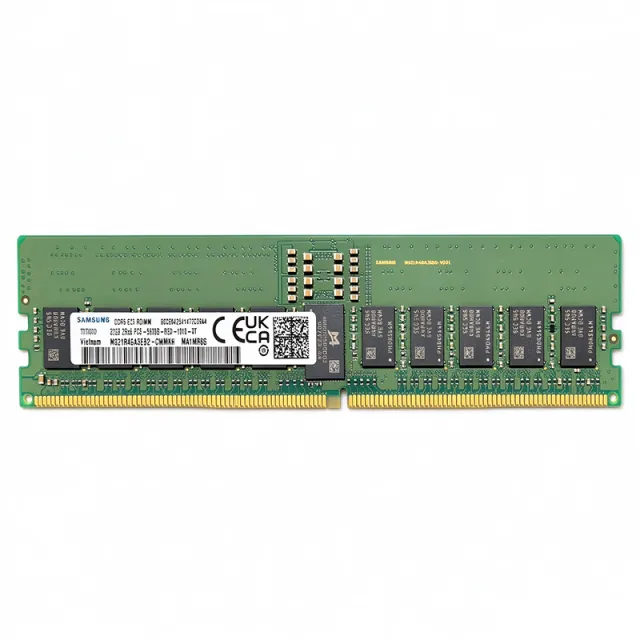
M321R4GA3EB2-CWM - 32GB DDR5-5600 ECC RDIMM | Samsung
The Samsung M321R4GA3EB2-CWM is a 32GB DDR5-5600 ECC registered DIMM (RDIMM) operating at 5600 MT/s (PC5-44800) on a 1.1V supply, built in a 288-pin dual-rank x8 (2Rx8) form factor for enterprise server platforms. An RDIMM (Registered DIMM) is a memory module that buffers the command and address signals through a register chip before they reach the DRAM devices, reducing electrical loading on the memory controller and enabling higher-capacity, higher-speed configurations than unbuffered memory. Within the memory hierarchy, RDIMM belongs to the family of registered/buffered server modules - above desktop UDIMMs and below load-reduced LRDIMMs - and is the standard choice for general-purpose 2-socket servers using Intel Xeon or AMD EPYC processors. Key features of the M321R4GA3EB2-CWM include its 32GB capacity organized as 2Rx8 with 20 pieces of 2Gx8 FBGA-packaged DRAM components, DDR5-5600 data rate for roughly 44.8 GB/s peak bandwidth per module, and CL46 CAS latency at the JEDEC-standard 1.1V operating voltage. On-die ECC (ODECC) plus registered parity and CRC protection deliver data integrity suitable for always-on infrastructure, and the 12nm-class E-die DRAM reduces parasitic capacitance and thermal dissipation compared with earlier lithographies. Architecturally, the module leverages DDR5 advances over DDR4, including a 12V module supply with an on-module PMIC regulating the 1.1V DRAM rail, doubled bank groups, and on-die ECC - improving signal integrity, power efficiency, and reliability at speed. Typical applications include data-center general-purpose servers, edge compute nodes, low-VM-density virtualization hosts, and enterprise workstations from vendors such as Dell PowerEdge, HPE ProLiant, Lenovo ThinkSystem, and Supermicro platforms that support PC5-44800R. Design and procurement consideration: DDR5 RDIMMs must be mixed only with modules of identical rank, organization, and speed per JEDEC population guidelines; always populate matched kits for optimal channel balance. This page synthesizes distributor pricing, drop-in alternatives, compatibility data, and practical design notes not found in the manufacturer datasheet.
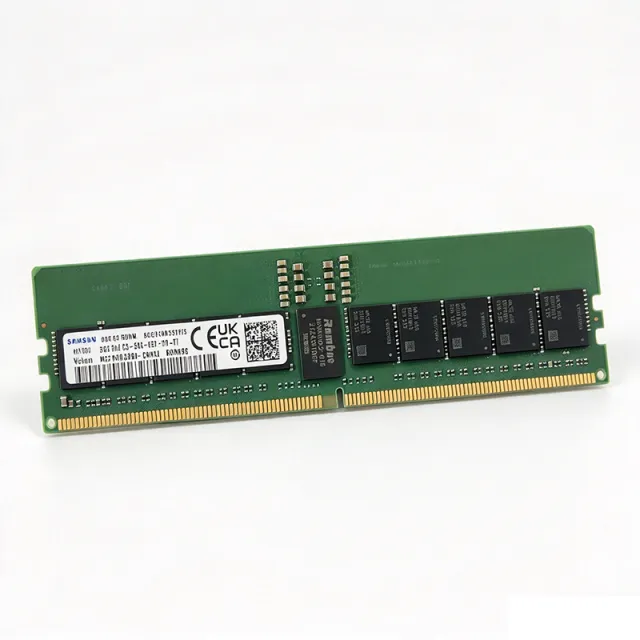
M321R4GA3PB0-CWM - 32GB DDR5-5600 ECC RDIMM | Samsung | Servers
The Samsung M321R4GA3PB0-CWM is a 32GB DDR5-5600 ECC registered DIMM (RDIMM) operating at 1.1V with a data rate of 5600 Mbps (PC5-44800) in a 288-pin registered DIMM form factor, organized as 2Rx8 dual-rank 4Gx72 with twenty 2Gx8 FBGA DDR5 DRAM components. A registered DIMM (RDIMM) is a server-class memory module that buffers the command and address signals through a register (RCD), reducing electrical load on the memory controller and enabling higher module counts per channel than unbuffered UDIMMs. Memory modules sit at the top of the DRAM hierarchy: DRAM chip -> FBGA-packaged component -> module (RDIMM/LRDIMM/SO-DIMM) -> memory subsystem, where RDIMMs dominate enterprise servers and workstations. On-die ECC (ODIECC) and registered operation make them mandatory in platforms such as Intel Xeon Scalable and AMD EPYC. Key features include DDR5-5600 speed with CL46 latency, 1.1V standard DDR5 operating voltage (reducing power versus DDR4's 1.2V), dual-rank x8 organization for strong memory bandwidth, and 288-pin RDIMM form factor with side-band management via SPD hub (SPD5118-class). The module is JEDEC-compliant for plug-and-play operation in qualified servers. The DDR5 architecture splits each module into two independent 32-bit subchannels, doubling effective concurrent access versus DDR4, and moves the power management IC (PMIC) onto the module for tighter voltage regulation at 1.1V. On-die ECC corrects internal DRAM cell errors before they reach the register level, complementing link ECC in registered operation. Typical applications include general-purpose enterprise servers (Dell PowerEdge, HPE ProLiant, Lenovo ThinkSystem), edge compute nodes with low VM density, workstations, and cloud infrastructure memory pools. Verified qualified platforms for this MPN include Lenovo ThinkSystem SR630 V3, SR650 V3, SR650 V4 and SD650 V3 (e.g., Lenovo 4X77A95267 cross-reference). Design consideration: always populate memory channels symmetrically per the server qualified vendor list (QVL); mixing RDIMM ranks or speeds forces all modules to the slowest common profile. This page synthesizes distributor inventory, drop-in alternatives, qualified-server cross references, and practical design notes not found in the manufacturer datasheet.

MT25QL01GBBB1EW9-0SIT - 1Gb SPI NOR Flash 133MHz | Micron
The Micron Technology MT25QL01GBBB1EW9-0SIT is a 1 Gbit (128 MB) 3V multiple I/O serial NOR flash memory with a 133 MHz SPI Quad I/O interface, operating from -40C to +85C in an 8-pin W-PDFN (8x6 mm, MLP8) exposed-pad package. Its FBGA code is RW256, and it supports x1, x2, and x4 I/O widths. Serial NOR flash is a nonvolatile memory category that stores code and data while allowing byte-level random access over a simple serial bus. In the system hierarchy, it sits under nonvolatile semiconductor memory, alongside parallel NOR and NAND flash, and is typically the boot device for processors, microcontrollers, and FPGAs. The SPI (Serial Peripheral Interface) bus with multiple I/O options reduces pin count and PCB footprint versus parallel NOR while maintaining fast code-execution performance. Key features of the MT25Q family include quad I/O (QSPI) operation at up to 133 MHz, which yields a peak transfer rate well above legacy single-lane SPI devices, plus 4 KB, 32 KB, and 64 KB sector erase granularity for efficient in-field firmware updates. The 1 Gbit density supports large feature-rich code images, and the 8x6 WDFN with exposed pad keeps the footprint small while providing good thermal and ground performance. The device operates from a 2.7 V to 3.6 V supply (nominal 3 V) and requires 4-byte addressing to access the full 128 MB address space, an important firmware consideration versus 3-byte-addressing lower-density parts. Standard SPI commands, dual/quad output reads, and eXecute-In-Place style fast reads make it suitable for direct code shadowing and XIP operation. Typical applications include FPGA configuration storage (Xilinx, Intel/Altera), MCU code and parameter storage, networking line-card firmware, and industrial HMI or instrumentation data logging where high density and nonvolatile reliability matter. Design consideration: verify that your host controller supports 4-byte addressing and that the JEDEC ID read is used at boot, since serial NOR devices from different vendors respond with different JEDEC IDs and register maps. This page synthesizes distributor pricing, drop-in alternative analysis, and practical design notes not found in the manufacturer datasheet.
MT25QL01GBBB8E12-0AUT - 1Gb SPI NOR Flash 133MHz | Micron
The Micron MT25QL01GBBB8E12-0AUT is a 1 Gbit (128 MB) multiple I/O SPI serial NOR Flash memory operating at 3 V with a 133 MHz clock, housed in a 24-ball T-PBGA (6x8 mm) package, and is AEC-Q100 qualified for the automotive temperature range of -40C to +125C. Serial NOR Flash is a nonvolatile memory class that stores code and data on a standard SPI-compatible bus (single, dual, and quad I/O). It sits within the memory hierarchy as a serial NOR device - a sibling of parallel NOR, and a code-storage counterpart to serial NAND and DRAM - and is typically used as boot memory for processors, FPGAs, and microcontrollers. Execute-in-place (XIP) allows the host CPU to run code directly from the device without copying to RAM. Key features of the MT25Q family part include a 133 MHz SPI clock with dual- and quad-I/O commands, 4KB/32KB/64KB sector erase granularity, XIP functionality, advanced write protection mechanisms, and extended (4-byte) address access for the full 1 Gbit density. The MT25QL01GBBB is a double-die (DDP) construction internally organized as 256M x4 / dual 512Mb dice. The device is validated for automotive platforms under Micron's automotive program (the -0AUT suffix and AEC-Q100 status per the Newark listing reflect this), and the FBGA code RW319 identifies the die/package combination. Random-access read latency and page-program performance support fast boot and OTA update workloads. Typical applications include automotive infotainment and ADAS boot flash, FPGA configuration storage, industrial PLC code memory, and networking equipment firmware storage where 1 Gbit code storage with quad-SPI bandwidth is required. Design consideration: the 24-ball BGA requires reflow assembly and X-ray inspection; plan the 4-byte addressing mode early because 1 Gbit exceeds the 128 MB boundary of 3-byte addressing. Power-rail decoupling and HOLD/RESET handling should follow the manufacturer datasheet. This page synthesizes distributor pricing, same-brand drop-in density/voltage variants, and practical design notes not found in the manufacturer datasheet.

MT25QL128ABB1ESE-0AUT - 128Mb SPI NOR Flash 133MHz AEC-Q100 | Micron
The Micron Technology MT25QL128ABB1ESE-0AUT is a 128 Mbit (16 MB) MT25Q family serial NOR flash memory with SPI, Dual SPI and Quad I/O interfaces operating at up to 133 MHz, in an 8-pin SOIC (8-SO W) package, rated for the automotive -40C to +125C temperature range. A serial NOR flash memory is a nonvolatile storage device that stores code and data in a NOR array accessed over a serial peripheral interface (SPI). In the system hierarchy, it sits under nonvolatile memory ICs, within the broader memory and storage semiconductor category, and typically serves as boot memory or firmware storage for microcontrollers, processors, and FPGAs. Key features of the MT25QL128ABB1ESE-0AUT include 133 MHz Quad SPI operation with a 5 ns access time, x1, x2, and x4 I/O organization (128M x1, 64M x2, 32M x4), and a 2.7V to 3.6V supply range. Hardware and software write protection, write-enable latching, and absolute write protection safeguard firmware integrity, while power-on reset protection prevents corrupt writes during brownout conditions. The MT25Q architecture provides fast random access for execute-in-place (XIP) code shadowing and boot code storage. Endurance is rated at 100,000 program/erase cycles per the device specifications, with 20-year data retention, meeting the reliability demands of automotive and industrial environments. The device is AEC-Q100 qualified and RoHS compliant, distinguishing it from commercial-grade serial flash variants. Typical applications include firmware boot storage for automotive ECUs and ADAS modules, embedded logging in industrial controllers, code storage for computing and networking modules, and replacement sourcing for legacy serial NOR sockets. The 133 MHz quad interface keeps boot times low even for large code images. For design-in, decouple VCC with a 0.1uF ceramic capacitor placed close to pin 8, and tie the HOLD#/IO3 and WP#/IO2 pins appropriately for the chosen bus width to avoid accidental write protection or hold-state entry during quad operation. This page adds value beyond the manufacturer datasheet by synthesizing distributor pricing, drop-in same-family alternatives, application guidance, and FAQ content in one place for engineers and buyers. All pricing references are as of 2026-09-01.
MT25QL256ABA8E12-0AUT - 256Mb SPI NOR Flash 133MHz | Micron
The Micron Technology MT25QL256ABA8E12-0AUT is a 256 Mbit (32 MB) multiple I/O serial NOR flash memory with SPI quad I/O support up to 133 MHz clock (5 ns clock period), a 2.7 V to 3.6 V supply range, and an AEC-Q100 qualified operating temperature of -40C to +125C, housed in a 24-ball T-PBGA (6x8 mm, FBGA code RW326) package. A serial NOR flash memory is a non-volatile storage device that stores code and data while retaining content without power, accessed over a serial peripheral interface (SPI). Within the memory hierarchy, it sits in the broader NOR flash family alongside parallel NOR, and in power-management/system terms it typically serves as the boot and code-execution memory for a microcontroller, FPGA, or application processor. Serial NOR is favored when pin count, board space, and in-place code execution (XIP) matter more than raw write bandwidth. Key features of the MT25QL256ABA8E12-0AUT include 256 Mb density organized as x1/x2/x4 (single, dual, and quad I/O), a maximum clock frequency of 133 MHz for fast code fetch, and an automotive-grade temperature rating that supports under-hood and other harsh environments. Micron's MT25Q architecture adds multiple I/O command sets (fast read dual output, quad output, and quad I/O) that increase effective read bandwidth beyond standard SPI without changing the pin count. The device is fabricated in Micron's NOR flash process with sector-erase and page-program architecture, hardware and software write protection, and power-on reset protection - features cited on distributor pages for this family. The 5 ns clock-cycle timing at 133 MHz supports execute-in-place boot code for processors that cannot tolerate the latency of loading code into RAM. Typical applications include FPGA configuration/boot storage, automotive ECU and ADAS code storage, industrial drives and networking equipment boot ROM, and set-top-box or display firmware storage where AEC-Q100 qualification and a wide -40C to +125C range are required. Design consideration: the 24-ball BGA package requires accurate land-pattern layout and X-ray or optical inspection capability for rework; confirm the SPI mode and command set compatibility with the host controller before second-sourcing. This page synthesizes distributor pricing, drop-in alternatives, and practical design notes not found in the manufacturer datasheet.
MT25QL256BBB8E12-CAUT - 256Mb SPI Quad I/O NOR Flash | Micron
The Micron Technology MT25QL256BBB8E12-CAUT is a 256Mb (32 MB) serial NOR flash memory with a multiple-I/O SPI (Quad SPI) interface, a 133 MHz maximum clock frequency with 5 ns clock period, and a supply voltage range of 2.7V to 3.6V, housed in a 24-ball thin fine-pitch ball grid array (24-T-PBGA / TBGA, 6x8 mm, FBGA code RW346). Serial NOR flash is a non-volatile memory category within the broader memory IC hierarchy (semiconductor -> non-volatile memory -> flash -> NOR flash -> serial/QSPI NOR flash). It stores code and data that must be execute-in-place (XIP) capable, offering byte-level random access and superior reliability compared to NAND flash, at the cost of lower density and higher cost per bit. QSPI NOR flash is the de facto boot memory for most embedded processors. Key features of the MT25Q family include x1, x2, and x4 (Quad) I/O data widths for up to 532 MB/s effective read throughput in Quad mode, an operating temperature range of -40C to +125C for industrial and automotive-adjacent environments, and a dedicated 64-byte OTP area outside the main memory array. Selected part numbers in the family provide an additional dedicated reset pin for improved system robustness. The MT25QL256 device architecture is based on Micron's advanced NOR process, with a uniform 64 KB (sector) / 4 KB (subsector) erase organization supporting fast in-field firmware updates. The BGA package delivers excellent electrical performance for high-speed signal integrity at 133 MHz clock rates and a compact 6x8 mm footprint for space-constrained designs such as FPGA configuration storage and embedded processors. Typical applications include FPGA and microcontroller boot/code storage (notably Xilinx and other FPGA bitstream storage), automotive infotainment and telematics code memory, industrial PLC and networking equipment firmware storage, and set-top box / display panel boot flash. Design consideration: because the 24-ball BGA footprint is not field-replaceable, verify reflow profile and PCB pad geometry against the Micron package data sheet, and reserve a reset/hold strategy to avoid bus contention during power sequencing. This page synthesizes distributor pricing, drop-in same-family alternatives, and practical design notes not found in the manufacturer datasheet.
MT29F4G01ABBFD12-AUT:F - 4Gbit SLC SPI NAND Flash | Micron
The Micron Technology MT29F4G01ABBFD12-AUT:F is a 4 Gbit (512 MB) single-level cell (SLC) serial NAND flash memory IC with an SPI interface, supplied in the automotive-grade suffix :F package (lead-free, RoHS-compliant TBGA) and rated for extended automotive temperature ranges per the AUT grade designation. Serial NAND flash is a category of non-volatile memory that stores data in floating-gate cells arranged in NAND strings but exposes a reduced-pin-count SPI (Serial Peripheral Interface) bus instead of the wide parallel asynchronous bus of conventional NAND. In the memory hierarchy, it sits between raw parallel NAND (highest throughput, complex controller requirement) and NOR flash (fast random read, lower density), offering designers a simple, low-pin-count path to high-density code and data storage. Key features of this device include 4 Gbit SLC density organized for reliable page-level operation, an SPI-compatible serial interface that drastically reduces pin count and PCB routing complexity compared to parallel NAND, and integrated ECC handling on-die that offloads error correction from the host, reducing firmware complexity. The :F suffix denotes Micron's automotive-qualified lead-free finishing option. Architecturally, the device organizes the 4 Gbit array into pages and blocks with on-die ECC and standard SPI command protocols (including quad-capable read operations on the BFD variant family), supporting fast sequential reads for code shadowing and data logging. SLC technology delivers substantially higher endurance and data retention than MLC or TLC NAND, which is why SLC serial NAND dominates automotive and industrial storage designs. Typical applications include automotive infotainment and telematics data storage, ADAS event data recorders, industrial programmable logic controllers, network equipment boot storage, and IoT gateways requiring high-endurance flash with minimal host pin usage. When designing this part in, reserve adequate VCC decoupling and honor the SPI mode timing requirements; because the :F suffix parts are automotive-qualified, follow Micron's automotive reliability guidelines for wear-leveling to exploit the full SLC endurance budget. This page synthesizes distributor pricing, drop-in same-family alternatives, and practical design notes not found in the manufacturer datasheet.
MX25L51245GXDI-08G - 512Mbit SPI NOR Flash 166MHz | Macronix
The Macronix MX25L51245GXDI-08G is a 512Mbit (64 MByte) 3V CMOS serial NOR Flash memory with Quad I/O, QPI, and DTR (Double Transfer Rate) support, running at up to 166 MHz in a 24-ball CSPBGA (6x8) package. It is organized as 64M x 8-bit and operates from a 2.7V to 3.6V supply. Serial NOR Flash is a non-volatile memory category within the broader flash memory hierarchy (NOR Flash -> flash memory -> semiconductor memory -> non-volatile memory IC). Unlike parallel NOR, serial NOR devices communicate over an SPI (Serial Peripheral Interface) bus, trading raw bandwidth for a much smaller pin count, smaller footprint, and lower system cost. Serial NOR is the dominant boot memory technology for embedded processors, FPGAs, microcontrollers, and networking SoCs. Key features of the MX25L51245G family include the MXSMIO (Serial Multi I/O) interface supporting x1, x2, and x4 I/O operation, QPI (Quad Peripheral Interface) mode for reduced command overhead, and DTR (Double Transfer Rate) mode that transfers data on both clock edges to maximize sequential read throughput. The device offers 100,000 program/erase cycles endurance and 20-year data retention per Macronix data. Technical depth: the XDI-08G speed grade supports a 166 MHz clock in Quad/DTR modes, enabling high read bandwidth for XIP (execute-in-place) code shadowing and fast FPGA configuration loading. Page program time is 750 microseconds with 60-microsecond word program support, and the architecture supports sector and block erase for flexible firmware update management. Typical applications include FPGA configuration/boot memory for Xilinx and Intel devices, embedded processor code storage in networking equipment, set-top boxes and automotive infotainment, and firmware storage in industrial controllers where high-density non-volatile code storage is required. Design consideration: verify VCC ramp and use the RESET#/hold features per the Macronix datasheet to ensure correct power-up state, and allocate proper decoupling at the 2.7V-3.6V supply pins. This page synthesizes distributor pricing, drop-in alternatives, pinout guidance, and practical design notes not found in the manufacturer datasheet alone.

N24RF04DWPT3G - Dual Interface 4Kb EEPROM RFID NFC Tag | onsemi
The onsemi N24RF04DWPT3G is a dual-interface RFID/NFC tag IC with a 4 Kb EEPROM, an ISO/IEC 15693 contactless RF interface at 13.56 MHz, and an I2C contact interface operating from 1.8 V to 5.5 V, housed in an 8-pin SOIC (0.154 in, 3.90 mm width) package. A dual-interface EEPROM tag belongs to the family of memory ICs that combine passive radio-frequency access with a wired bus. The RFID/NFC tag hierarchy runs: dual-interface EEPROM tag -> RFID transponder IC -> RF memory IC -> memory IC -> semiconductor. The N24RF04 allows a reader (contactless, energy harvesting from the RF field) and a host microcontroller (contact, externally powered) to access the same non-volatile memory, enabling board-level identification, configuration storage, and traceability. Key features include the 4 Kb (512-byte) EEPROM organized with user and system blocks, ISO/IEC 15693 and ISO 18000-3 protocol support, NFC Forum Type 5 tag interoperability, an energy-harvesting output that can power small companion circuits, and data verification mechanisms for write integrity. The I2C interface requires an external supply and supports standard bus communication with any microcontroller, according to the onsemi N24RF04 datasheet. Technically, the device rectifies the 13.56 MHz carrier from the reader antenna coil connected between the AC0 and AC1 pins, regulates it to an internal supply, and manages read/write cycles to the EEPROM with error checking. The dual-interface arbitration ensures memory consistency regardless of which port accesses the data, a critical feature when both a reader and an MCU may write the same blocks. Typical applications include consumable identification and authentication in printers and medical cartridges, board-level manufacturing traceability, parameter storage for replaceable modules, and NFC-enabled configuration of industrial and IoT devices. When designing, keep the antenna loop close to the AC0/AC1 pins and respect the I2C supply requirement: the contact interface cannot rely on harvested field energy. Choose pull-up values for SDA/SCL appropriate to the 1.8 V to 5.5 V supply domain. This page synthesizes distributor pricing, drop-in alternatives, and practical design notes not found in the manufacturer datasheet.

N25Q032A13EV7A0 - 32Mb SPI NOR Flash 108MHz | Micron
The Micron Technology N25Q032A13EV7A0 is a 32Mbit SPI NOR Flash memory IC operating at up to 108 MHz clock frequency, supplied at 2.7V to 3.6V, housed in an 8-lead VDFPN8 (MLP8) surface-mount package. NOR Flash is a non-volatile memory type in which each cell connects in parallel to bit lines, enabling true random access for code execution in place (XIP). Within the memory hierarchy, NOR Flash sits alongside NAND Flash under non-volatile semiconductor memory; where NAND stores bulk data, NOR Flash stores boot code and firmware that microprocessors execute directly from the array. SPI (Serial Peripheral Interface) NOR devices reduce pin count versus parallel NOR, simplifying board routing for embedded designs. Key features of the N25Q032A13EV7A0 include the 32Mbit (4MB) density organized for 8M x 4 die, a 108 MHz maximum SPI clock supporting double data rate and dual/quad I/O operation for fast code download, and a wide 2.7V to 3.6V supply range compatible with standard 3.3V systems. The device supports industrial-grade temperature from -40C to +125C per distributor data, allowing use in harsh environments. Architecturally, this device belongs to Micron's N25Q (P-Stim / e-Memory) family of high-performance SPI NOR Flash, which adds paging support, subsector erase granularity and fast program/erase timing. Standard commands cover read, page program, sector and bulk erase with status polling via the status register. Typical applications include firmware and boot code storage for industrial controllers, networking equipment configuration memory, automotive infotainment modules, and set-top box boot devices where reliable XIP execution is required. Design consideration: keep SPI clock loading low and add series damping resistors on SCK when running at 108 MHz to limit signal integrity issues; verify erase/program cycles against the specified endurance in the manufacturer datasheet. This page synthesizes distributor availability, drop-in family alternatives, and practical design notes not found in the manufacturer datasheet.
N25Q064A13EF8A0E - 64Mb SPI NOR Flash 108MHz | Micron
The Micron N25Q064A13EF8A0E is a 64 Mb (8 MB) 3 V multiple I/O serial NOR Flash memory supporting SPI clock rates up to 108 MHz, manufactured on 65 nm NOR technology and housed in an 8-pin VDFPN (MLP8, 8 x 6 mm) exposed-pad package. A serial NOR Flash is a nonvolatile memory device that stores code and data and is read over a serial bus (SPI) using a memory-mapped execute-in-place (XIP) model. In the system hierarchy, NOR Flash occupies the code-storage tier between boot ROM and DRAM/NAND mass storage, providing random access for direct code execution without copying to RAM first. Key features of the N25Q064A13EF8A0E include 64 Mb density, 108 MHz SPI operation in standard, dual, and quad I/O modes, and an automotive-grade temperature profile. The multiple I/O architecture reduces instruction overhead and improves effective read bandwidth compared to single-I/O SPI Flash, accelerating boot times in embedded processors. The exposed-pad DFN package provides good thermal and electrical grounding and a compact 8 x 6 mm footprint. Technically, the device uses 65 nm NOR floating-gate technology with sector and block erase organization, program/erase suspend capability, and XIP modes that allow the host controller to execute code directly from the Flash array. Power-up and power-down behavior, rescue sequences, and AC reset specifications are fully documented in the manufacturer datasheet to ensure deterministic system startup. Typical applications include BIOS/code storage in embedded x86 and ARM systems, boot firmware for networking equipment, automotive telematics and infotainment modules, and FPGA configuration storage where quad-SPI read bandwidth shortens configuration time. Design consideration: keep SPI trace lengths short and matched for quad-I/O operation at 108 MHz, and verify power-up timing against the datasheet power-up requirements to avoid false device lockout states. This page synthesizes distributor pricing, verified drop-in alternatives, pinout data, and practical design notes in one place - information not consolidated in the manufacturer datasheet alone.

N25Q064A13ESFA0F - 64Mb 108MHz SPI NOR Flash | Micron
The Micron Technology N25Q064A13ESFA0F is a 64Mb (8 MB) 3V multiple-I/O SPI serial NOR flash memory with a maximum clock rate of 108 MHz and a 16-pin SOIC wide body (400-mil) package. It supports standard SPI, dual SPI, and quad SPI interfaces, and is qualified to AEC-Q100 for automotive applications with an operating temperature range of -40C to +125C. Serial NOR flash is a nonvolatile memory technology that stores code and data in a NOR array accessible over a simple serial peripheral interface. Within the memory hierarchy, it sits alongside parallel NOR and NAND flash as a member of the flash memory family, and is the dominant choice for boot code storage because it offers random-access read behavior, high reliability, and XIP (execute-in-place) capability from a very small pin count. Key features of this device include 64Mb density organized as 64M x 1, 32M x 2, or 16M x 4 depending on the interface mode; a 4KB sector erase granularity that reduces erase overhead for parameter storage; and quad I/O operation that delivers effective read bandwidth far beyond legacy single-bit SPI. An accelerated program/erase path and deep power-down mode minimize system power, and hardware RESET# support improves system recoverability. Technically, the N25Q family uses advanced NOR floating-gate cells with 3V single-supply operation. Command set compatibility with the widely used 25-series convention, page programming, block (64KB) and sector (4KB) erases, and status-register-based polling simplify driver development. The device also supports XIP mode activation with confirmation bit settings, as described in the manufacturer datasheet. Typical applications include automotive ECU boot code storage, firmware storage for industrial PLCs and networking equipment, BIOS storage in embedded x86 systems, and parameter storage in medical and test instruments. The 108 MHz quad SPI interface makes it well matched to MCUs and SoCs with quad-SPI memory controllers. Design consideration: verify that the controller drive strength and PCB trace length support 108 MHz quad SPI signaling, and always reserve access to RESET# for field recoverability. This page synthesizes distributor pricing context, drop-in alternative analysis, pinout, and practical design notes not found in the manufacturer datasheet alone.
N25Q128A13ESFA0F - 128Mb SPI NOR Flash 108MHz | Micron
The Micron Technology N25Q128A13ESFA0F is a 128 Mbit (16 MB) 3 V multiple-I/O serial NOR flash memory with a 108 MHz SPI bus interface, 4-Kbyte subsector erase granularity, and XiP (execute-in-place) support, housed in a 16-pin wide-body SOIC (SO W, 300 mil) surface-mount package. Serial NOR flash is a nonvolatile memory category that stores code and data while allowing byte-level random access over a serial peripheral interface. Within the memory hierarchy, it sits between parallel NOR flash (faster but pin-hungry) and serial NAND (cheaper but block-accessed). Serial NOR is the dominant boot-memory choice for embedded processors because code can execute directly from the array (XiP) or be shadowed to RAM at power-up, with only four to six signals required. Key features of the N25Q128A13ESFA0F include 128 Mbit density organized as 16M x 8, support for standard, dual, and quad SPI protocols that double and quadruple effective bandwidth, 4-Kbyte subsector erase on boot sectors for fine-grained parameter storage, and a clock speed up to 108 MHz with fast access time (7 ns class per distributor listings). The device operates from a single 3V/3.3V supply, supporting the standard industrial memory rail. Architecturally, the N25Q family (originally developed by Numonyx, later acquired by Micron) uses a multi-I/O SPI front end with command-set compatibility extended for dual-output, dual-I/O, quad-output, and quad-I/O read modes. This lets host controllers trade pin count for throughput: quad-I/O operation at 108 MHz yields an effective transfer rate several times higher than conventional single-SPI serial flash, enough to meet XiP boot-time targets in embedded Linux and RTOS systems. Typical applications include code storage for FPGAs and CPLDs, boot flash for embedded processors and SoCs, BIOS/firmware storage in networking equipment, and configuration memory in industrial automation and telecommunications line cards. The quad-SPI interface and XiP support make it a natural match for Xilinx-style configuration streams and memory-mapped execution on Cortex-class MCUs. Design consideration: when running quad-I/O reads at 108 MHz, keep SPI trace lengths short and matched, and verify that the HOLD#/DQ3 pin is driven correctly, because in quad mode it functions as an active data line rather than a hold control. This page synthesizes distributor pricing, drop-in alternatives, pinout guidance, and practical design notes not found in the manufacturer datasheet, and is verified as of 2026-09-02.
N25Q256A13EF8A0F - 256Mb SPI NOR Flash 108MHz | Micron
The Micron N25Q256A13EF8A0F is a 256Mb (32MB) 3V multiple I/O serial NOR Flash memory delivering up to 108 MHz SPI clock operation in an 8-pin VDFPN (MLP8, 8x6 mm) package. It supports x1, x2, and x4 I/O width via single, dual, and quad SPI protocols, and operates from -40C to +85C. Serial NOR Flash is a nonvolatile memory category that stores code and data while allowing byte-level random read access over a simple serial peripheral interface. In the system hierarchy it sits below parallel NOR and NAND Flash in pin count and board area, making it the dominant boot-memory choice for embedded processors, microcontrollers, and FPGAs where a compact footprint and high reliability outweigh raw density. Key features include 108 MHz maximum clock frequency with 8 ns access timing, 4KB sector erase granularity that reduces update latency and wasted erase cycles, multiple I/O (SPI, dual-SPI, quad-SPI) protocols that cut instruction overhead and boost effective read bandwidth, and a 3V to 3.6V single supply. The VDFPN exposed-pad package improves thermal and ground performance over standard SOIC-8 while remaining footprint-compatible in most layouts. The device is manufactured on Micron's 65nm NOR technology, the first generation of Micron's high-performance multiple I/O serial Flash family. Subsector erase of 4KB sectors enables fine-grained parameter storage, while block (64KB) and full-chip erase options support bulk reprogramming. A hardware write-protect pin (W#/VPP_DQ2) allows software-controlled sector locking and protects the boot region against accidental corruption. Typical applications include FPGA configuration bitstream storage, embedded processor boot code, BIOS/UEFI firmware in industrial PCs, automotive instrument clusters, and networking equipment line cards. Quad-SPI mode makes the device especially well matched to Intel/Altera and Xilinx configuration flows. Design consideration: respect the 100K program/erase cycle endurance per sector in firmware by implementing wear-leveling or sector rotation for frequently updated parameters, and decouple VCC with 0.1uF close to pin 2. This page synthesizes verified distributor data, drop-in same-family alternatives, pinout detail, and practical design notes not found in the manufacturer datasheet.
N25Q256A13ESFA0F - 256Mb SPI NOR Flash 108MHz | Micron
The Micron N25Q256A13ESFA0F is a 256 Mbit (32 MB) SPI-compatible serial NOR Flash memory manufactured on 65 nm NOR technology, operating from a 2.7 V to 3.6 V supply at up to 108 MHz in a 16-pin SOP2 (SOP-II) surface-mount package. It supports single, dual, and quad I/O SPI protocols for x1/x2/x4 data widths. Serial NOR Flash is a non-volatile memory class that stores code and data while allowing in-system byte-wise reads through a low-pin-count SPI bus. In the memory hierarchy it sits between parallel NOR (higher pin count, faster random access) and serial NAND or EEPROM (lower endurance, slower random access), making it the default boot memory for embedded processors, microcontrollers, and FPGAs. Key features include a 108 MHz maximum clock frequency with equivalent dual- and quad-I/O throughput, 4 KB sector erase granularity for fine-grained wear management, execute-in-place (XIP) capability so code can run directly from the Flash without copying to RAM, and advanced write-protection mechanisms. The 65 nm SLC NOR cell design delivers high reliability and fast random read latency versus charge-trap alternatives. Architecturally, the N25Q256A device organizes 256 Mbit as 32 M x 8 with sector, subsector, and page program operations, using an SPI-compatible instruction set familiar from the broader N25Q family. The multiple-I/O bus and XIP mode minimize boot time in deeply embedded systems, while the standard SPI commands simplify software reuse across density grades. Typical applications include FPGA and MCU boot code storage, automotive and industrial embedded systems, networking equipment firmware, and set-top-box or display code storage, where 32 MB of reliable code memory with quad-SPI bandwidth is required. Design consideration: when running at 108 MHz in quad mode, pay close attention to signal integrity on DQ lines and keep trace lengths matched; confirm the required output drive and dummy-cycle configuration per the manufacturer datasheet. This page synthesizes distributor pricing context, drop-in same-package alternatives, pinout, and practical design notes not found in a single manufacturer document.
N25Q256A83ESFA0F - 256Mb SPI NOR Flash 108MHz | Micron
The Micron Technology N25Q256A83ESFA0F is a 256 Mbit (32 MB) 3V multiple I/O serial NOR flash memory with an SPI-compatible bus operating at up to 108 MHz, housed in a 16-pin wide SOIC (SOIC-16 W) surface-mount package with industrial operating temperature range of -40C to +125C. A serial NOR flash memory is a non-volatile storage IC that stores code and data on NOR cells and communicates over a serial SPI bus (single, dual, or quad I/O). Within the memory hierarchy, it sits alongside parallel NOR, NAND flash, and EEPROM as a class of non-volatile memory ICs, and is the standard choice for execute-in-place (XIP) boot code because it offers random access with low pin count. Key features of the N25Q256A83ESFA0F include 256 Mbit density organized as 32M x 8, quad SPI (multiple I/O) data throughput at 108 MHz clock rates, 4 KB sector erase granularity for flexible code management, and advanced write-protection mechanisms. The device is manufactured on Micron's 65nm NOR technology, the first generation of the high-performance N25Q family. Architecturally, the N25Q supports execute-in-place (XIP) operation, allowing the host processor to run code directly from the flash without copying to RAM first. The SPI-compatible interface supports standard single-I/O, dual-I/O, and quad-I/O commands, and the extended temperature rating makes the part suitable for harsh industrial environments. Memory array organization uses sectors and subsectors for erase operations and page programming for writes. Typical applications include boot code storage in industrial controllers, embedded processors and FPGAs, networking equipment storing firmware images, and automotive-adjacent telematics or display modules where wide temperature tolerance is required. When designing with this part, verify that your host SPI controller supports the command set and that hold and reset functions are correctly terminated; upper address bits beyond the 24-bit boundary are accessed through extended address registers. Decouple VCC with 0.1uF ceramic capacitors close to pin 2. This page synthesizes distributor pricing, verified specifications, same-family drop-in alternatives, and practical design notes not found together on the manufacturer datasheet alone.