Товары (38.000+)

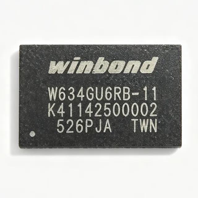
W634GU6RB-11 - 4Gb DDR3L SDRAM 933MHz | Winbond
W634GU6RB-11

W634GU6RB-11 - 4Gb DDR3L SDRAM 933MHz | Winbond

The W634GU6RB-11 is a 4Gbit DDR3L SDRAM memory IC from Winbond Electronics, organized as 256M x 16 bits. It operates at a clock frequency of 933 MHz (DDR3L-1866) with a CAS latency of 20 ns, and is supplied in a 96-ball VFBGA (7.5x13 mm) package. This device is designed for low-power applications, operating from a 1.35V supply (1.283V to 1.45V range), and supports parallel interface with a data rate of 1866 MT/s. DDR3L (Double Data Rate 3 Low Voltage) SDRAM is a type of synchronous dynamic random-access memory that transfers data on both edges of the clock signal, effectively doubling the data rate. It is a low-voltage variant of DDR3, operating at 1.35V instead of the standard 1.5V, reducing power consumption by about 20% compared to standard DDR3. DDR3L is part of the DDR SDRAM family, which includes DDR, DDR2, DDR3, and DDR4, and is widely used in computing, networking, and embedded systems where high bandwidth and low power are critical. Key features of the W634GU6RB-11 include auto self-refresh, auto precharge, data mask, write leveling, ZQ calibration, asynchronous reset, and dynamic on-chip termination (ODT). These features enhance signal integrity and simplify system design. The device supports a temperature range of -40°C to +95°C, making it suitable for industrial applications. It is RoHS compliant and halogen-free, aligning with environmental standards. Technically, the W634GU6RB-11 utilizes a 96-ball VFBGA package with a 7.5x13 mm footprint, offering a compact solution for space-constrained designs. The 20 ns CAS latency ensures fast access times, while the 933 MHz clock speed provides high bandwidth for data-intensive tasks. The device includes on-die termination (ODT) to improve signal quality on the memory bus, and supports write leveling for improved timing margins in multi-rank configurations. Typical applications include networking equipment (routers, switches), industrial computing, embedded systems, and consumer electronics such as set-top boxes and smart TVs. Its low voltage and high density make it ideal for power-sensitive designs where performance and efficiency are balanced. When designing with this device, ensure proper decoupling capacitors are placed near the VDD and VDDQ pins to minimize noise. Also, follow the JEDEC DDR3L layout guidelines for signal integrity, especially for high-speed signals. The device supports a 1.35V supply, so verify that the power management IC provides a stable 1.35V rail.

USD $13,52 Контакты
W634GU6RB-11TR - 4Gb DDR3L SDRAM 933MHz | Winbond
W634GU6RB-11TR

W634GU6RB-11TR - 4Gb DDR3L SDRAM 933MHz | Winbond

The W634GU6RB-11TR is a 4Gbit DDR3L SDRAM memory IC from Winbond Electronics, organized as 256M x 16 bits. It operates at a clock frequency of 933 MHz (DDR3L-1866) with a CAS latency of 13, and features a parallel interface with a 20 ns access time. The device is housed in a compact 96-ball VFBGA (7.5x13 mm) package, making it suitable for space-constrained applications requiring high memory density. DDR3L (Double Data Rate 3 Low Voltage) SDRAM is a type of synchronous dynamic random-access memory that operates at a lower voltage (1.35V) compared to standard DDR3 (1.5V), reducing power consumption by up to 20% while maintaining similar performance. It is part of the memory hierarchy in computing systems, serving as the main working memory for processors, and is widely used in laptops, embedded systems, networking equipment, and industrial applications. Key features of the W634GU6RB-11TR include support for 1.35V operation (with 1.5V compatibility), auto self-refresh, auto precharge, data mask, write leveling, ZQ calibration, asynchronous reset, and dynamic on-chip termination (ODT). These features enhance signal integrity and simplify system design. The device is RoHS compliant and halogen-free, meeting environmental standards. Technically, the W634GU6RB-11TR uses a 96-ball VFBGA package with a 0.8mm ball pitch, providing excellent thermal and electrical performance. The 933 MHz clock rate enables data rates up to 1866 MT/s, delivering high bandwidth for demanding applications. The device supports a temperature range of -40°C to +95°C, making it suitable for industrial environments. Typical applications include embedded computing, networking routers and switches, industrial automation, and high-performance consumer electronics. Its low voltage and high density make it ideal for power-sensitive designs. When designing with this memory, ensure proper decoupling capacitors near the VDD and VDDQ pins, and follow the PCB layout guidelines in the datasheet to minimize signal integrity issues at high speeds.

Запрос цены Контакты
W634GU6RB-12 - 4Gb DDR3L SDRAM x16 933MHz | Winbond
W634GU6RB-12

W634GU6RB-12 - 4Gb DDR3L SDRAM x16 933MHz | Winbond

The W634GU6RB-12 is a 4Gbit DDR3L SDRAM from Winbond Electronics, organized as 256M x 16, operating at 1.35V with a parallel interface. It is housed in a 96-ball VFBGA (7.5x13mm) package and supports DDR3L-1600 (11-11-11) speed grade at 933 MHz clock. This memory IC is designed for high-bandwidth applications requiring low power consumption and high reliability. DDR3L SDRAM is a type of double data rate synchronous dynamic random-access memory that operates at a lower voltage (1.35V) compared to standard DDR3 (1.5V), reducing power consumption by up to 20% while maintaining similar performance. It is part of the DDR3 memory family, which uses 8n-prefetch architecture and on-die termination to achieve high data rates. DDR3L is widely used in mobile, embedded, and industrial systems where power efficiency is critical. Key features include a 4Gbit density, x16 organization, 933 MHz clock speed (DDR3L-1600), 20 ns tRCD, and a 96-ball VFBGA package. The device supports industrial temperature grades: the -12I grade guarantees -40°C to 95°C case temperature, and the -12J grade guarantees -40°C to 105°C. It is RoHS compliant and halogen-free, meeting environmental standards. The W634GU6RB-12 utilizes advanced DRAM process technology, offering high-speed data transfer with low power consumption. The 8n-prefetch architecture enables burst lengths of 8, and the on-die termination (ODT) improves signal integrity. The device includes programmable CAS latency, burst length, and output drive strength, providing flexibility for system optimization. Typical applications include networking equipment, industrial automation, embedded computing, and consumer electronics such as set-top boxes and smart TVs. The low voltage and high density make it ideal for space-constrained designs requiring large memory capacity. When designing with this device, ensure proper decoupling capacitors near the VDD and VDDQ pins, and follow the PCB layout guidelines in the datasheet to minimize signal integrity issues. The device requires a 1.35V supply and a separate VDDQ supply, which should be well-regulated.

Запрос цены Контакты
W634GU6RB09I - 4Gb DDR3L SDRAM x16 1066MHz | Winbond
W634GU6RB09I

W634GU6RB09I - 4Gb DDR3L SDRAM x16 1066MHz | Winbond

The W634GU6RB09I is a 4Gbit DDR3L SDRAM memory IC from Winbond Electronics, organized as 256M x 16 bits. It operates at a clock frequency of 1.067 GHz (DDR3L-2133) with a CAS latency of 20 ns, and is housed in a 96-ball VFBGA (7.5x13 mm) package. This device is designed for low-voltage operation at 1.35V, making it suitable for power-sensitive applications such as mobile devices, embedded systems, and networking equipment. DDR3L (Double Data Rate 3 Low Voltage) is a type of synchronous dynamic random-access memory (SDRAM) that operates at 1.35V, reducing power consumption by about 20% compared to standard DDR3 (1.5V). It is part of the DDR3 family, which uses double data rate signaling to transfer data on both edges of the clock, achieving high bandwidth. DDR3L is widely used in laptops, servers, and industrial applications where energy efficiency is critical. Key features include a 4Gbit density, x16 data bus width, 1.067 GHz maximum clock speed, and industrial temperature range (-40°C to +95°C). The device supports burst lengths of 8 and 4, on-die termination (ODT), and programmable CAS latency. It is RoHS compliant and lead-free, meeting environmental standards. Technically, the W634GU6RB09I uses a 96-ball VFBGA package with a 0.8mm ball pitch, enabling high-density mounting on PCBs. The memory core is based on advanced DRAM process technology, providing high reliability and performance. The device includes auto-refresh and self-refresh modes for low-power standby, and supports DLL (Delay-Locked Loop) for precise timing. Typical applications include embedded computing, networking routers, industrial automation, and consumer electronics such as set-top boxes and smart TVs. Its low voltage and high density make it ideal for designs requiring large memory capacity with minimal power draw. When designing with this component, ensure proper decoupling capacitors near the power pins and follow the layout guidelines in the datasheet to minimize signal integrity issues. The device requires a 1.35V supply and a separate VDDQ for I/O, which should be regulated accurately.

Запрос цены Контакты
W634GU6RB09J - 4Gb DDR3L SDRAM x16 1066MHz | Winbond
W634GU6RB09J

W634GU6RB09J - 4Gb DDR3L SDRAM x16 1066MHz | Winbond

The Winbond W634GU6RB09J is a 4Gbit DDR3L SDRAM organized as 256M x 16, operating at 1.35V with a data rate of 1066MHz (DDR3L-2133). It comes in a 96-ball VFBGA (7.5x13mm) package, offering a compact footprint for space-constrained designs. This memory IC is designed for high-bandwidth applications requiring low power consumption, making it ideal for mobile, embedded, and networking systems. DDR3L (Double Data Rate 3 Low Voltage) is a type of synchronous dynamic random-access memory (SDRAM) that operates at 1.35V, reducing power consumption by about 20% compared to standard 1.5V DDR3. It is part of the DDR3 family, which uses double data rate signaling to transfer data on both edges of the clock, achieving high throughput. DDR3L is backward-compatible with DDR3 and is widely used in laptops, servers, and industrial electronics where energy efficiency is critical. Key features include a 4Gbit density, x16 organization, 1.067 GHz clock speed, and a CAS latency of 20 ns. The device supports on-die termination (ODT), programmable CAS latency, and burst lengths of 8 and 4. It operates over a temperature range of 0°C to +95°C (case temperature) and is RoHS compliant. The 96-VFBGA package measures 7.5x13mm with a 0.8mm ball pitch, enabling high-density PCB layouts. Technically, the W634GU6RB09J uses a 30nm-class process technology, achieving low power and high speed. It features internal calibration for ZQ, write leveling, and read leveling to ensure signal integrity at high frequencies. The device supports auto-refresh and self-refresh modes, reducing standby power. Its low voltage operation and advanced power management make it suitable for battery-powered devices. Typical applications include mobile computing, networking equipment, industrial automation, and consumer electronics such as set-top boxes and smart TVs. The high density and low power make it ideal for systems requiring large memory capacity with minimal energy consumption. When designing with this component, ensure proper decoupling capacitors near the power pins and follow the layout guidelines in the datasheet to maintain signal integrity at 1066MHz. The device requires a 1.35V supply and a separate VDDQ, which should be regulated accurately.

Запрос цены Контакты
W634GU6RB11I - 4Gb DDR3L SDRAM x16 933MHz | Winbond
W634GU6RB11I

W634GU6RB11I - 4Gb DDR3L SDRAM x16 933MHz | Winbond

The W634GU6RB11I is a 4Gbit DDR3L SDRAM memory IC from Winbond Electronics, organized as 256M x 16 bits. It operates at a clock frequency of 933 MHz (DDR3L-1866) with a CAS latency of 20 ns, and is supplied in a 96-ball VFBGA package measuring 7.5 x 13 mm. This device is designed for low-voltage operation at 1.35V, reducing power consumption by approximately 15% compared to standard 1.5V DDR3, making it ideal for power-sensitive applications. DDR3L SDRAM (Double Data Rate 3 Low Voltage) is a type of synchronous dynamic random-access memory that transfers data on both edges of the clock signal, effectively doubling the data rate. It operates at a lower voltage (1.35V) than standard DDR3 (1.5V), offering improved energy efficiency. DDR3L is part of the DDR SDRAM family, which includes DDR, DDR2, DDR3, and DDR4, and is widely used in computing, networking, and embedded systems where high bandwidth and low power are critical. Key features of the W634GU6RB11I include a parallel interface with a 16-bit data bus, support for industrial temperature range (-40°C to +95°C), and compatibility with JEDEC DDR3L standards. The device offers burst lengths of 8 and 4, on-die termination (ODT), and programmable CAS latency. Its low-voltage operation and high density make it suitable for applications requiring large memory capacity with minimal power draw. The W634GU6RB11I utilizes advanced DRAM process technology, achieving high-speed data transfer while maintaining low power consumption. The 96-ball VFBGA package provides excellent thermal and electrical performance, with a compact footprint suitable for space-constrained designs. The device supports auto-refresh and self-refresh modes, ensuring data integrity with minimal power consumption during idle periods. Typical applications include networking equipment (routers, switches), industrial automation, embedded computing, and consumer electronics such as set-top boxes and smart TVs. Its industrial temperature rating makes it suitable for harsh environments, while the low-voltage operation extends battery life in portable devices. When designing with this component, ensure proper decoupling capacitors are placed near the power pins to minimize noise. The VFBGA package requires careful PCB layout to route the fine-pitch balls, and the DDR3L interface should be terminated according to JEDEC guidelines to maintain signal integrity.

Запрос цены Контакты
W634GU6RB11J - 4Gb DDR3L SDRAM x16 933MHz | Winbond
W634GU6RB11J

W634GU6RB11J - 4Gb DDR3L SDRAM x16 933MHz | Winbond

The Winbond W634GU6RB11J is a 4Gbit DDR3L SDRAM organized as 256M x 16, operating at a clock frequency of 933 MHz (DDR3L-1866) with a data rate of 1866 MT/s. It is housed in a 96-ball VFBGA package (7.5x13 mm) and operates from a 1.35V supply, making it suitable for low-power applications. The device supports parallel interface with a burst length of 8 and features a 20 ns CAS latency. DDR3L (Double Data Rate 3 Low Voltage) is a type of synchronous dynamic random-access memory (SDRAM) that operates at 1.35V, reducing power consumption by about 20% compared to standard DDR3 (1.5V). It is part of the DDR3 family, which uses double data rate signaling to transfer data on both edges of the clock, achieving high bandwidth. DDR3L is commonly used in mobile devices, embedded systems, and industrial applications where power efficiency is critical. Key features include auto self-refresh, auto precharge, data mask, write leveling, ZQ calibration, asynchronous reset, and dynamic on-chip termination (DTC). These features enhance signal integrity and simplify system design. The device supports industrial temperature range from -40°C to +95°C, making it suitable for harsh environments. It is RoHS compliant and halogen-free, aligning with environmental standards. Technically, the W634GU6RB11J uses a 96-ball VFBGA package with a 0.8mm ball pitch, providing excellent thermal and electrical performance. The memory array is organized in 8 banks, and the device supports programmable CAS latency (CL) and additive latency (AL) for flexible timing. The on-die termination (ODT) feature improves signal quality by matching impedance, reducing reflections on the data bus. Typical applications include networking equipment, industrial automation, medical devices, and embedded computing systems where high-density, low-power memory is required. The 4Gb density and x16 organization make it ideal for applications needing moderate memory capacity with a wide data bus. When designing with this device, ensure proper decoupling capacitors near the VDD and VDDQ pins to minimize power supply noise. Also, follow the JEDEC DDR3L layout guidelines for signal integrity, including controlled impedance traces and proper termination.

Запрос цены Контакты
W634GU6RB12I - 4Gb DDR3L SDRAM x16 800MHz | Winbond
W634GU6RB12I

W634GU6RB12I - 4Gb DDR3L SDRAM x16 800MHz | Winbond

The W634GU6RB12I is a 4Gbit DDR3L SDRAM organized as 256M x 16, operating at 1.35V with a data rate of 800MHz (DDR3L-1600). It is housed in a 96-ball VFBGA (7.5x13mm) package and is designed for industrial temperature range (-40°C to +95°C). This memory IC is ideal for applications requiring high-density, low-power volatile storage. DDR3L (Double Data Rate 3 Low Voltage) is a type of synchronous dynamic random-access memory (SDRAM) that operates at 1.35V, reducing power consumption by about 20% compared to standard DDR3 (1.5V). It is part of the DDR3 family, which uses double data rate signaling to transfer data on both edges of the clock, achieving high bandwidth. DDR3L is commonly used in computing, networking, and embedded systems where power efficiency is critical. Key features include a parallel interface with 800MHz clock speed, 20ns row cycle time, and support for industrial temperature grades. The device is RoHS compliant and halogen-free, meeting environmental standards. The 96-ball VFBGA package offers a compact footprint suitable for space-constrained designs. The W634GU6RB12I utilizes advanced DRAM process technology, providing reliable performance with low power consumption. It supports standard DDR3L features such as on-die termination (ODT), programmable CAS latency, and burst lengths of 8. The industrial temperature grade ensures operation in harsh environments. Typical applications include industrial automation, networking equipment, embedded computing, and automotive infotainment systems. Its high density and low power make it suitable for memory-intensive tasks in these domains. When designing with this device, ensure proper decoupling and signal integrity practices are followed, as high-speed memory interfaces require careful PCB layout to minimize noise and reflections.

Запрос цены Контакты
W634GU6RB12J - 4Gb DDR3L SDRAM 933MHz | Winbond
W634GU6RB12J

W634GU6RB12J - 4Gb DDR3L SDRAM 933MHz | Winbond

The W634GU6RB12J is a 4Gbit DDR3L SDRAM from Winbond Electronics, organized as 256M x 16 and operating at 1.35V. It features a parallel interface with a clock speed of 933 MHz (DDR3L-1866) and a CAS latency of 20 ns. The device is housed in a 96-ball VFBGA package (7.5x13 mm) and is designed for high-bandwidth memory applications. DDR3L SDRAM is a type of dynamic random-access memory that operates at a lower voltage (1.35V) compared to standard DDR3 (1.5V), reducing power consumption while maintaining high data rates. It is part of the DDR3L memory family, which is widely used in computing, networking, and industrial applications where power efficiency is critical. Key features include a 4Gbit density, x16 organization, 933 MHz clock speed, and support for the DDR3L-1866 specification. The device offers a burst length of 8 and supports on-die termination (ODT) for improved signal integrity. It operates over a temperature range of -40°C to +105°C (TCASE) for the 12J industrial plus grade, making it suitable for harsh environments. The W634GU6RB12J utilizes advanced DRAM process technology to achieve high speed and low power. It includes features such as programmable CAS latency, write leveling, and self-refresh modes to optimize performance and power consumption. The 96-ball VFBGA package provides excellent thermal and electrical performance. Typical applications include embedded systems, networking equipment, industrial automation, and automotive infotainment. The low voltage and high speed make it ideal for power-sensitive designs that require high memory bandwidth. When designing with this device, ensure proper decoupling and signal integrity practices are followed. The DDR3L interface requires careful PCB layout to minimize crosstalk and maintain signal quality at high speeds.

Запрос цены Контакты
W681308DG - USB Audio Controller 16-bit 48-LQFP | Nuvoton
W681308DG

W681308DG - USB Audio Controller 16-bit 48-LQFP | Nuvoton

The Nuvoton W681308DG is a USB audio controller IC with an integrated 16-bit audio codec, housed in a 48-pin LQFP (7x7 mm) surface-mount package. As a member of the Winbond/Nuvoton W6813 series of USB audio controllers, it integrates a USB controller, audio codec, and embedded microcontroller into a single chip for USB audio peripheral designs. A USB audio controller is a mixed-signal device that implements the USB audio class protocol on the digital side and an audio codec (codec = coder-decoder) on the analog side. Within the system hierarchy, it sits between a general-purpose USB microcontroller and a dedicated audio codec: it handles USB enumeration, audio streaming, clocking, and sample-rate conversion, while also providing microphone and speaker signal paths. This integration reduces bill-of-materials count compared to a discrete USB MCU plus external codec solution. Key features of the W681308DG include a 16-bit audio data path, USB full-speed audio transport, integrated microphone and speaker audio channels, and a compact 7x7 mm 48-LQFP footprint that supports consumer peripheral form factors. The device operates from a 3.3 V supply, consistent with the family datasheet description of the W681308 series as a 3.3 V part. Architecturally, the W681308 combines an 8-bit CISC microcontroller core with on-chip program memory and a hardwired USB audio function block. The codec front end handles anti-aliasing filtering, ADC for microphone inputs, and DAC for speaker outputs, while the MCU firmware manages HID interfaces, mute/volume controls, and other USB descriptor behavior. Refer to the manufacturer datasheet for precise clock, PLL, and interface specifications. Typical applications include USB headset and headphone amplifiers, desktop microphone arrays, USB speakerphones, VoIP handsets, and general USB audio dongles where a single-chip, low-cost USB audio solution is required. A key design consideration is analog layout: the microphone preamp and DAC outputs are sensitive to digital return-path noise, so a solid ground plane, careful separation of analog and digital traces, and proper decoupling of the 3.3 V rail per the manufacturer datasheet recommendations are essential for a low-noise result. This page synthesizes distributor sourcing data, datasheet references, and practical design notes not found in the manufacturer datasheet.

Запрос цены Контакты
W77C032A40FL - 40MHz 8-Bit ROMless MCU | Nuvoton
W77C032A40FL

W77C032A40FL - 40MHz 8-Bit ROMless MCU | Nuvoton

The Nuvoton W77C032A40FL is a ROMless Turbo-51 8-bit microcontroller operating at up to 40 MHz, with 1K x 8 bits of RAM, 36 I/O pins, and a 44-pin BQFP package. Designed for embedded control applications, the device combines a high-clock-speed 8051-compatible core with an internal oscillator, allowing designers to build compact control systems without adding an external program-memory device. An 8-bit microcontroller is a semiconductor integrated circuit containing a central processing unit, memory, I/O ports, and peripheral functions on one package. In the product hierarchy, it belongs to the microcontroller family of embedded processors and embedded ICs. The W77C032A40FL belongs to the Turbo-51 family and uses a ROMless architecture, meaning program storage must be supplied by external memory while working data can be held in its internal RAM. Key characteristics include a maximum clock frequency of 40 MHz, 1K x 8-bit SRAM, and 36 general-purpose I/O lines. Its internal oscillator reduces the external clock-component count, while the 44-BQFP package exposes substantially more I/O than smaller dual-inline or small-outline packages. These characteristics make the MCU appropriate for compact controllers with multiple discrete inputs and outputs, particularly where an 8051-compatible instruction set and external program memory are required. The W77C032A40FL is positioned as a ROMless Turbo-51 device rather than a self-contained MCU with embedded Flash. External program memory and interface circuitry therefore influence the complete memory system. Its 36 I/O pins provide ample connectivity for control signals, indicators, relays, sensors, and communication peripherals. Because the device is specified at 40 MHz, firmware timing, memory-access delays, peripheral clock requirements, and external-memory interface timing must be reviewed together during schematic and PCB design. Typical applications include industrial machine controls, building-control modules, appliance controllers, interface modules, and other embedded automation products. The combination of 36 I/O, internal RAM, and external program-memory support is especially useful when a product needs substantial I/O breadth but limited on-chip volatile memory. The MCU can act as the supervisory controller between sensors, actuators, communications circuitry, and discrete logic. A key design consideration is that ROMless operation requires careful implementation of the external memory interface and correct timing for the selected memory device. Place decoupling close to the supply pins, route oscillator and memory signals consistently, and keep high-current switching nodes away from sensitive control inputs. Confirm pin multiplexing, reset behavior, and peripheral availability against the manufacturer datasheet before finalizing firmware and board connections. This page consolidates the principal electrical, memory, package, sourcing, and replacement information for W77C032A40FL. It also provides practical application guidance and design checks that help engineers determine whether this ROMless Turbo-51 MCU fits a control design before committing to PCB layout and external-memory implementation.

Запрос цены Контакты
W77C032A40PL - 40MHz ROMless 8051 MCU | Nuvoton
W77C032A40PL

W77C032A40PL - 40MHz ROMless 8051 MCU | Nuvoton

The Nuvoton Technology Corporation W77C032A40PL is an 8-bit ROMless 8051-compatible microcontroller operating at up to 40 MHz, with 1 KB x 8 RAM, 36 I/O lines, and a 44-pin PLCC package. The device uses the W77C032 Turbo-51 processor architecture, which reduces wasted instruction cycles and executes 8051 instructions approximately 1.5 to 3 times faster than a traditional 8051 core at the same clock speed. A microcontroller is a programmable semiconductor integrating a processor core, memory, I/O ports, timers, serial communications, and interrupt functions on one integrated circuit. The W77C032 belongs to the 8-bit MCU hierarchy and retains 8052 pin and instruction-set compatibility. Because the part is ROMless, application firmware must be supplied through external program-memory hardware, making the device suitable for systems that require flexible code storage, boot loading, field updating, or shared memory among several devices. The principal specifications include a 40 MHz maximum operating speed, 1 KB x 8 internal RAM, four 8-bit I/O ports, 36 total I/O lines, and an internal oscillator. The W77C032 also incorporates standard 8052 resources, including three 16-bit timer/counters, a full-duplex serial port, and multiple interrupt sources. Its 4.5 V to 5.5 V operating range and 44-PLCC package support established 5 V embedded-control architectures where a leaded, socket-compatible footprint is preferable to a fine-pitch surface-mount package. The redesigned processor core avoids wasted clock and memory cycles, improving execution efficiency without changing the familiar 8051 instruction set. This combination is useful when maintaining legacy 8051 source code while increasing control-loop or peripheral-handling performance. Since the MCU has no on-chip program memory, a system designer must account for external ROM or another memory source when creating the memory map, boot sequence, and firmware-loading architecture. Typical uses include industrial controllers, embedded data-acquisition equipment, communications controllers, legacy 8051 peripheral upgrades, and compact automation modules. The 36 I/O lines provide substantial parallel-interface capacity, while the timers and serial port reduce the need for external peripheral chips. Board-level designs should also provide a stable clock or oscillator arrangement, external program-memory interfacing, suitable decoupling, and adequate pin-compatible routing. A key design consideration is that the PLCC package has 44 positions, but the verified product records do not provide a complete numbered pin description. Engineers should therefore assign the PCB footprint and nets directly from the pin table and package drawing in the manufacturer data sheet rather than inferring connections from generic 8051 diagrams. Confirm the external-memory interface, reset behavior, clock requirements, and available I/O before finalizing the board layout. This product summary consolidates the confirmed architecture, memory, clock, package, sourcing, and lifecycle information with engineering guidance for external-memory implementation, firmware compatibility, and PLCC layout. It also distinguishes directly documented characteristics from parameters that still require confirmation from the complete manufacturer data sheet.

Запрос цены Контакты
W77E058A40FL - 40MHz 8051 32KB Flash MCU | Nuvoton
W77E058A40FL

W77E058A40FL - 40MHz 8051 32KB Flash MCU | Nuvoton

Nuvoton Technology Corporation W77E058A40FL is an 8-bit CMOS W77-series microcontroller with 32 KB of embedded Flash memory, a 40 MHz operating frequency, and a 44-BQFP package. It uses a four-clock machine-cycle 8051-compatible architecture and operates from a 5 V supply, combining legacy MCS-51 software compatibility with substantially faster instruction execution than the original standard 80C51 family. An 8051-compatible microcontroller is an embedded processor designed around the MCS-51 instruction set and its associated register, interrupt, timer, serial-interface, and port architecture. The W77 series places that established software ecosystem within the broader hierarchy of embedded controllers, 8-bit microcontrollers, and general-purpose semiconductor devices. This makes it useful for control systems that benefit from established 8051 tools and code while requiring higher processing throughput and integrated Flash rather than an external program-memory device. The W77E058A40FL combines several headline characteristics: 8-bit processing, 40 MHz operation, and 32 KB of embedded Flash. Its four-clock machine-cycle design executes each machine cycle in a quarter of a full 40 MHz clock period. The device also provides four 8-bit I/O ports and follows the MCS-51 instruction set, allowing engineers to reuse familiar driver concepts and peripheral-control code while selecting a faster Flash-based implementation. Technically, the part belongs to the W77 family and is positioned as a compact, 5 V embedded controller. Its Flash memory consolidates program storage on the die, simplifying the hardware arrangement compared with an architecture that requires external program memory. Because the controller remains compatible with the MCS-51 instruction set, software migration from an appropriate 80C52-class design can be easier than moving to a different instruction set. Board compatibility still requires verification of pin functions, electrical limits, memory organization, and peripheral availability. Typical applications include industrial keypad and panel controllers, motor and relay-sequencing modules, compact instrumentation, appliance-control boards, and legacy 8051 peripheral upgrades. The 40 MHz execution rate can improve responsiveness in polling loops, protocol handling, and time-dependent control tasks, while the four 8-bit I/O ports support digital input, output, and external-interface connections when the remaining pins provide the required clock, reset, and power functions. A key design consideration is that pin-compatible software does not automatically prove drop-in electrical compatibility. Before replacing an existing 8051 device, verify the 44-BQFP footprint, pin assignments, reset behavior, operating voltage, oscillator connections, I/O drive limits, and peripheral functions against the current datasheet. Programming and development-tool requirements should also be checked because instruction-set compatibility does not guarantee that every legacy programmer supports the device. This product page combines the W77E058A40FL's core specifications, verified component listings, application guidance, design checks, and a transparent comparison of candidate cross-reference devices. It also distinguishes confirmed drop-in options from merely similar controllers, helping engineers make a replacement decision without relying on package similarity alone.

Запрос цены Контакты
W77E058A40PL - 40MHz 8051 MCU, 32KB Flash | Nuvoton
W77E058A40PL

W77E058A40PL - 40MHz 8051 MCU, 32KB Flash | Nuvoton

Nuvoton Technology Corporation W77E058A40PL is an 8-bit CMOS 8051-compatible microcontroller operating at up to 40 MHz, with 32KB of Flash memory in a 44-pin PLCC package. It executes four clocks per machine cycle, provides two UART devices and two DPTR registers, and operates from a 5 V supply across the 4.5 V to 5.5 V range. The W77E058A family is also pin-compatible with traditional 12T 8051 devices. An 8051 microcontroller is an embedded-computing IC that combines a CPU core, program memory, data memory, I/O ports, and peripherals on one integrated circuit. Within the product hierarchy, the W77E058A is an 8-bit MCU, a 4T 8051 MCU, a member of the MCS-51 instruction-set family, and a member of the broader embedded processor and semiconductor categories. Its 8051 compatibility supports established compiler, debugger, and application-development ecosystems. Key features include a 40 MHz maximum operating frequency, a four-clock machine-cycle architecture, and 32KB of on-chip Flash organized as 32K by 8 bits. Two UART devices support serial communication, while two DPTR registers provide separate 16-bit pointer contexts. Four 8-bit I/O ports support digital interfaces, and the 4.5 V to 5.5 V operating range aligns the device with conventional 5 V embedded equipment. The device uses an 8-bit CISC architecture compatible with the MCS-51 instruction set and remains compatible with traditional 12T 8051 interfaces. Its 4T architecture reduces the clock-to-machine-cycle ratio to four clocks, allowing 40 MHz operation without changing the fundamental software timing model. Because the product is identified as NRND, engineers should verify availability and consider the manufacturer's current portfolio before starting a new design. Typical applications include security and alarm systems, communication equipment, industrial control, power-management controllers, and industrial personal computers. The two UARTs are useful for sensor, transceiver, display, or host serial links, while the four parallel I/O ports can handle digital control signals, status indicators, relay logic, or keypad interfaces. The principal design consideration is the 5 V supply requirement and the limited 0°C to 70°C temperature range. Decoupling and signal-integrity practices remain important because all peripherals share the same supply and ground system. Engineers should also confirm the PLCC-44 footprint, pin assignments, and board-level clearances against the manufacturer datasheet before layout release. This page combines the manufacturer's family-level architecture and lifecycle information with distributor specifications and a practical replacement assessment. It also identifies the package, programming interface considerations, application fit, and design checks needed to evaluate the W77E058A40PL in an embedded control platform.

Запрос цены Контакты
W77E516A40FL - 40MHz 8051 MCU 64KB Flash | Nuvoton
W77E516A40FL

W77E516A40FL - 40MHz 8051 MCU 64KB Flash | Nuvoton

Nuvoton Technology Corporation W77E516A40FL is an 8-bit 8051-compatible microcontroller operating at 40 MHz with 64 KB of embedded Flash program memory in a 44-pin PQFP package. The device includes four 8-bit I/O ports, three 16-bit timer/counters, a full-duplex serial port, and interrupt resources inherited from the standard 8052 architecture. Its redesigned processor core removes wasted clock and memory cycles, allowing typical instructions to execute approximately 1.5 to 3 times faster than a traditional 8051 at the same crystal frequency. An 8051-compatible microcontroller is an embedded control processor that retains the classic 8051 instruction set while adding a redesigned execution core and modern integrated Flash memory. The W77E516 belongs to the 8-bit microcontroller hierarchy, where Flash program memory replaces externally attached ROM and supports compact, self-contained control systems. This combination makes the device suitable for industrial controllers, communication equipment, data-acquisition modules, and legacy equipment upgrades where existing 8051 software can be retained. The principal specifications are a 40 MHz operating speed, 64 KB of 64K x 8 Flash program memory, 1 KB of 8-bit RAM, 36 I/O lines, and a 5 V supply. Its 8052-compatible architecture provides four 8-bit I/O ports, three 16-bit timer/counters, a full-duplex UART, and multiple interrupt sources. The redesigned core improves instruction throughput without requiring a change to the standard 8051 instruction set, which helps designers reuse established firmware and peripheral-driver routines. Program execution benefits from a processor architecture that avoids wasted memory and clock cycles. Because the device is instruction-set compatible with the 8052, software can use standard 8051 development tools while taking advantage of the faster core. The integrated Flash memory consolidates program storage onto the device, reducing system-level component count and allowing firmware updates to be handled without a separate external memory device. Typical applications include industrial control panels, serial-interface adapters, test and measurement instruments, embedded data collectors, and communication modules. The 36 available I/O lines support peripheral connections, while the timer/counter and serial resources reduce the need for external interface components. The device is also appropriate for maintaining older 8051-based products where software compatibility is more valuable than migration to a different instruction set. The main design consideration is that the W77E516A40FL is an 8-bit, 5 V device rather than a low-power 3.3 V or modern 32-bit controller. Board designs should provide the specified 5 V operating supply, correct decoupling, and a stable clock source. Verify oscillator requirements, absolute maximum ratings, and timing margins in the manufacturer datasheet before laying out a new PCB, especially when replacing an electrically different original MCU. This page combines the manufacturer technical description, distributor specifications, packaging information, and practical guidance for evaluating the W77E516A40FL in 8051-compatible designs. It also identifies the scarcity of verified pin-compatible substitutes, providing a drop-in cross-reference candidate without presenting unverified components as equivalent parts.

Запрос цены Контакты
W77E532A40PL - 40MHz 8051 128KB Flash MCU | Nuvoton
W77E532A40PL

W77E532A40PL - 40MHz 8051 128KB Flash MCU | Nuvoton

The Nuvoton Technology Corporation W77E532A40PL is a 40 MHz, 8-bit 8051-compatible microcontroller with 128KB of program Flash, 1KB of RAM, 36 general-purpose I/O pins, and a 44-pin PLCC package. It operates from a single 5 V supply and executes the standard 8051 instruction set in a four-cycle architecture. An 8051-compatible microcontroller is an embedded controller that retains the classic 8051 programming model and peripheral structure while using an internally redesigned processor core. The W77E532A belongs to the W77 family of enhanced 8051 devices, providing compatibility with 8052 software and the hardware resources expected from a standard 8052, including four 8-bit I/O ports, three 16-bit timer/counters, a full-duplex serial port, and interrupt sources. Key device characteristics include a 40 MHz operating speed, 128KB of Flash program memory, 1KB of internal RAM, and 36 I/O pins. The redesigned core removes wasted clock and memory cycles, allowing instructions to complete approximately 1.5 to 3 times faster than a traditional 8051 at the same crystal frequency. A 5 V supply and 44-pin J-lead PLCC package make the device suitable for established embedded control platforms rather than new high-density mixed-signal designs. The W77E532A architecture remains instruction-set and 8052 pin compatible while improving execution efficiency. Its 128KB Flash area provides substantially more program storage than many classical 8051 controllers, reducing the need for external program memory in larger control routines. Integrated timers support periodic timing, event counting, and modulation tasks, while the serial port handles low-speed communication with external controllers or data acquisition modules. Typical uses include industrial controllers, data acquisition equipment, communications interfaces, embedded instrumentation, and legacy 8051 system upgrades. The device can also serve as a bridge between an established 8051 software base and a newer PCB revision, provided the board footprint, supply rail, oscillator arrangement, and peripheral assignments match the original controller. When designing around the W77E532A40PL, confirm the 5 V supply tolerance, external crystal or clock connection, Flash programming method, and reset configuration against the manufacturer datasheet. Because the PLCC package is legacy-oriented, it is less convenient than an LQFP or QFP package for automated assembly, hand soldering, or compact consumer products. This page consolidates device specifications, package information, application guidance, and verified same-footprint alternatives into a practical engineering reference. It also highlights where an engineer must confirm pin mapping, timing, and supply requirements before treating a candidate as a functional replacement.

Запрос цены Контакты
W77IC32A25PL - 25MHz ROMless 8051 MCU | Nuvoton
W77IC32A25PL

W77IC32A25PL - 25MHz ROMless 8051 MCU | Nuvoton

Nuvoton Technology Corporation W77IC32A25PL is an 8-bit ROMless W77 Turbo-51 microcontroller operating at 25 MHz, with 1K x 8 RAM, 36 I/O lines, and a 44-pin PLCC package. It is intended for embedded 8051-compatible control systems that require an external program-memory device while retaining a conventional 8-bit MCU architecture. A ROMless 8051 microcontroller is a variation of the MCS-51 microcontroller family in which the program memory is not integrated on the chip. The processor executes its firmware from external memory, allowing application-specific code capacity to be selected during system design. Within the semiconductor hierarchy, W77IC32A25PL belongs to the 8-bit microcontroller class, the broader embedded-processing category, and ultimately the microcontroller and semiconductor ecosystems. The device combines a 25 MHz clock with a 1K x 8 internal RAM array and 36 input/output lines. Its ROMless architecture is useful when firmware must exceed internal program-memory limits, when multiple products share the same external-memory configuration, or when code updates are managed outside the MCU. The -40°C to +85°C operating-temperature range supports industrial-temperature equipment while retaining compatibility with the established 8051 instruction set and peripheral environment. Technically, the W77 family is positioned as a Turbo-51 implementation, meaning that its clock rate is higher than that of the original 12 MHz 8051 class. At 25 MHz, the device offers greater instruction throughput than standard 8051 parts, although actual application performance depends on bus timing, wait states, external-memory access, and the selected memory architecture. The ROMless design makes external address decoding and code-memory interfacing central parts of the hardware design rather than optional functions. Typical uses include industrial controllers, appliance interfaces, embedded data-acquisition equipment, legacy 8051 peripheral boards, and control modules upgraded from slower standard 8051 processors. The broad I/O count allows the MCU to connect switches, displays, relays, sensors, and communication interfaces while the external program-memory bus accommodates larger firmware images. Designers should also account for the external memory interface timing when calculating system-level operating margins. PCB implementation requires a 44-pin PLCC land pattern, careful routing of the external program-memory bus, and decoupling close to the supply pins. Because the PLCC package is not represented by a dedicated diagram key in the XAIPART package library, use the manufacturer package drawing and pin-description table when assigning tracks. Confirm oscillator, reset, I/O, and memory-bus requirements against the manufacturer datasheet before releasing a layout. This product page combines the verified device identity, package and timing information, application guidance, drop-in comparison limits, and practical implementation cautions. It helps engineers determine whether the W77IC32A25PL fits a new 8051 design or whether an existing board requires qualified substitution and software validation.

Запрос цены Контакты
W77L032A25FL - 25MHz ROMless 8051 MCU | Nuvoton
W77L032A25FL

W77L032A25FL - 25MHz ROMless 8051 MCU | Nuvoton

Nuvoton Technology Corporation W77L032A25FL is an 8-bit ROMless 8051-compatible microcontroller operating at up to 25 MHz, with 1K x 8 RAM, 36 I/O lines, and a 44-BQFP package. It operates from 2.7 V to 5.5 V and uses an internal oscillator. The W77L032 core is designed to complete 8051 instructions faster than a traditional 8051 operating at the same clock speed. An 8051-compatible microcontroller is an embedded processor that implements the widely used MCS-51 instruction set and associated peripheral architecture. Within the embedded-control hierarchy, it belongs to the 8-bit MCU family and provides a simple alternative to larger 16-bit or 32-bit controllers when control logic, serial communications, timers, and limited data processing are the primary requirements. A ROMless device requires an external program-memory interface. Key characteristics include a 25 MHz maximum operating frequency, 1K x 8 bytes of internal RAM, 36 general-purpose I/O pins, and a 2.7 V to 5.5 V supply range. The device is intended for surface-mount assembly in a 44-BQFP package. Its ROMless architecture makes it useful when the application requires external program storage, configuration flexibility, or a larger memory arrangement than an on-chip ROM device provides. The W77L032 core is designed to reduce wasted instruction cycles relative to a conventional 8051 implementation. According to the manufacturer documentation, typical instruction execution can be approximately 1.5 to 3 times faster than a traditional 8051 at the same crystal frequency, depending on the instruction type. This improvement can shorten control-loop execution time without changing the software's 8051 instruction-level compatibility. Typical uses include industrial control panels, compact automation equipment, appliance controllers, serial-interface equipment, and embedded products that already use 8051-compatible code or peripherals. Designers should also consider the external program-memory interface and required memory type when laying out the PCB. For industrial and automotive contexts, verify qualification and operating-temperature requirements before committing the device to a production design. A key implementation consideration is that the external clock, reset, memory, and decoupling connections must follow the pin-assignment and electrical requirements in the W77L032/W77L032A/W77M032A datasheet. Confirm the external memory interface, reset behavior, and I/O allocation in the final schematic rather than deriving them from the package outline alone. This product page consolidates the verified device identity, core specifications, package details, sourcing options, and practical design guidance. It also separates the ROMless W77L032A configuration from related flash-based W77M032A devices, helping engineers compare memory architecture, clock requirements, and PCB compatibility before selection.

Запрос цены Контакты
W77L032A25PL - 25MHz ROMless 8051 MCU | Nuvoton
W77L032A25PL

W77L032A25PL - 25MHz ROMless 8051 MCU | Nuvoton

Nuvoton Technology Corporation W77L032A25PL is a ROMless 8-bit 8051-compatible microcontroller rated up to 25 MHz, supplied in a 44-pin PLCC package. It operates from 2.7 V to 5.5 V and provides 1K x 8 bits of RAM, an 8-bit data bus, and up to 36 I/O positions according to the catalog information. Its ROMless architecture separates execution storage from the controller, allowing the external program-memory configuration to be selected for the target application. An 8051 microcontroller is an 8-bit embedded-control component that combines a CPU core, memory interfaces, timers, serial communication, and parallel I/O. Within the product hierarchy, the W77L032 belongs to the 8051-compatible microcontroller family, which sits above general-purpose microcontrollers and below the broader category of embedded processors and semiconductors. The principal benefits of this device are its 25 MHz maximum clock, broad 2.7 V to 5.5 V supply range, and generous I/O count for a small 8-bit controller. ROMless operation is particularly useful when code storage must remain external or when a common controller can support several memory configurations. The 44-pin PLCC package also provides a leaded form factor that can simplify inspection, assembly, and prototyping compared with a very small surface-mount package. The W77 architecture uses an 8-bit data bus and provides 1K x 8 bits of RAM. One catalog entry identifies an internal oscillator, while another listing describes the ROM type as flash despite the primary product descriptions identifying the device as ROMless. Engineers should therefore consult the manufacturer datasheet and memory-interface section when confirming the exact external-memory configuration, oscillator arrangement, and timing characteristics for a production design. Typical applications include industrial controllers, serial-interface equipment, data acquisition modules, embedded keypads, motor-control interfaces, and legacy 8051 peripheral controllers. The combination of 36 I/O positions and a 25 MHz clock allows the device to coordinate multiple discrete inputs and outputs while retaining the straightforward programming model associated with 8051-compatible controllers. Design planning should begin with the 44-pin PLCC footprint, external program-memory requirements, oscillator connections, reset behavior, and the allocated I/O functions. Validate every pin against the current manufacturer datasheet before layout release, particularly where firmware depends on external memory timing or specific peripheral multiplexing. This product page consolidates the available electrical, package, sourcing, and replacement information into an engineering-focused selection guide. It also highlights the verified drop-in family options, application guidance, comparison limits, and design checks needed to evaluate the W77L032A25PL for an embedded-control design.

Запрос цены Контакты
W77L058A25FL - 8-Bit 80C51 32KB Flash 25MHz MCU | Nuvoton
W77L058A25FL

W77L058A25FL - 8-Bit 80C51 32KB Flash 25MHz MCU | Nuvoton

The Nuvoton Technology Corporation W77L058A25FL is an 8-bit flash microcontroller built on a 4-cycle 8051 core, with 32 KB of on-chip flash memory, a 25 MHz maximum operating frequency and a 2.7 V to 5.5 V supply range, packaged in a 44-pin MQFP (10 x 10 mm) surface-mount package. It targets cost-sensitive, high-volume consumer and industrial control designs that need a small footprint, wide supply tolerance and legacy 8051 toolchain compatibility. An 8-bit microcontroller (MCU) is a self-contained computing element that integrates a CPU core, program memory, data memory and peripherals onto a single die. The classic 8051 core, also called an MCS-51 or C51, remains the most widely installed 8-bit architecture in the industry, and its 4-cycle pipeline (rather than the original 12-cycle design) roughly triples instruction throughput compared with an early 8051. As a member of the wider microcontroller -> embedded processor -> semiconductor hierarchy, this part targets cost-sensitive embedded control rather than signal processing or connectivity. Key features of the W77L058A25FL include 32 KB of flash program memory for in-circuit programmable firmware, a 25 MHz clock rating that delivers up to 25 million instruction cycles per second, and a 2.7 V to 5.5 V operating range that covers both 3.3 V and 5 V system rails. Because the core is an 8051 derivative, existing assembly routines and Keil C51, SDCC or IAR 8051 toolchains can be reused without architectural rework, protecting firmware investment. The 44-pin MQFP (10 x 10 mm) footprint balances I/O count against board area, giving designs four 8-bit ports plus dedicated reset, clock and programming pins in a compact square surface-mount package suitable for automated assembly. As an MCU, the device integrates flash, RAM and standard 8051 peripherals (timers, serial ports and interrupt controller) on one die, eliminating the need for external program memory. Typical applications include small appliance and kitchen equipment controllers, LED driver and dimming modules, household meter and energy-monitoring front panels, industrial sequence controllers, keyboard and panel interface hubs, and compact sensor-node controllers where a 25 MHz 8051 core is sufficient and a 32 KB firmware budget is adequate. When designing around the W77L058A25FL, verify the pin multiplexing of each port against the peripheral assignment required by your firmware, and keep the decoupling network short: a 0.1 uF ceramic plus a 4.7 uF bulk capacitor at VDD/VSS minimizes brownout risk during flash write cycles. The 44-pin square outline also demands careful lead-frame tooling, so confirm the recommended land pattern and reflow profile before committing to volume production. This page consolidates distributor availability, pin- and package-matched drop-in alternatives from the same 8051 family, and practical layout and toolchain notes that go beyond the manufacturer datasheet.

Запрос цены Контакты
W77L516A25PL - 25MHz 8-Bit 8051 MCU, 64KB Flash | Nuvoton
W77L516A25PL

W77L516A25PL - 25MHz 8-Bit 8051 MCU, 64KB Flash | Nuvoton

The Nuvoton Technology Corporation W77L516A25PL is an 8-bit 8051-compatible microcontroller operating at 25 MHz, with 64 KB of flash program memory, 1 KB of RAM, and 36 I/O lines in a 44-pin PLCC package. It combines the familiar 8052 instruction set with a redesigned processor core that executes instructions approximately 1.5 to 3 times faster than a traditional 8051 at the same clock frequency. The W77L516A25PL is designed for embedded-control applications requiring deterministic serial communication, timer resources, parallel I/O, and programmable flash storage. An 8-bit microcontroller is a compact processor intended to control embedded systems rather than execute a desktop operating system. Within the semiconductor hierarchy, the W77L516A25PL belongs to the 8051-compatible microcontroller class and retains the standard 8052 peripheral model, including four 8-bit I/O ports, three 16-bit timer/counters, a full-duplex serial port, and interrupt resources. Its instruction-set compatibility allows legacy 8051-oriented code and development practices to be retained during product modernization. The principal device characteristics include 64 KB of flash program memory, 1 KB of on-chip RAM, 36 I/O pins, and a 25 MHz operating frequency. Additional integrated resources identified for this device include a serial port, power-on reset, and a watchdog timer. The redesigned core removes wasted clock and memory cycles, so software timing can improve without changing the external clock speed. Flash memory also provides a more flexible program-storage medium than mask-programmed or one-time-programmable microcontroller implementations. The 44-pin PLCC package provides a leaded, socket-compatible format suited to controllers, interface modules, industrial control boards, and legacy system upgrades. Its pin-compatible 8052 heritage simplifies board-level continuity when a design moves from a conventional 8051-class controller to this faster implementation. Designers should still validate the clock configuration, peripheral allocation, reset behavior, and memory map in the target system rather than assuming every legacy peripheral behaves identically. Typical uses include industrial equipment interfaces, serial protocol bridges, data acquisition modules, appliance controllers, embedded instrumentation, and communication adapters. The combination of four parallel I/O ports, three timers, serial communications, and 36 I/O lines is especially useful for systems that must connect switches, sensors, displays, relays, and legacy peripherals while maintaining predictable control timing. The principal design consideration is preserving compatibility at both software and board level. Confirm that the chosen oscillator and reset circuit meet the datasheet requirements, allocate every pin according to the manufacturer's pin description, and include adequate decoupling. Because this is a legacy-compatible 8-bit architecture, migration planning should also include confirmation of compiler support, bootloader behavior, peripheral register mapping, and any source-code changes required for the faster core. This page combines the manufacturer's device data with practical selection guidance, application context, package information, and verified sourcing links. It is intended to help engineers determine whether the W77L516A25PL fits an existing embedded-control design and how to evaluate compatible W77-family options without overlooking memory, timing, package, or toolchain requirements.

Запрос цены Контакты
W77L532A25FL - 8-Bit 128KB Flash MCU | Nuvoton
W77L532A25FL

W77L532A25FL - 8-Bit 128KB Flash MCU | Nuvoton

The Nuvoton W77L532A25FL is an 8-bit embedded microcontroller with 128KB of Flash program memory, 36 I/O pins, and a 25 MHz maximum operating frequency. It is packaged in a 44-pin BQFP and includes an 8051 core, serial-port connectivity, a power-on reset peripheral, and a watchdog timer. The device is identified as an active part and is positioned for compact embedded-control designs that require nonvolatile firmware storage and a broad external bus interface. An 8-bit microcontroller is a semiconductor integrated circuit designed to execute embedded instructions using an 8-bit data path. The W77L532A25FL belongs to the 8051-compatible microcontroller hierarchy, combining a CPU core, Flash memory, RAM, serial communication, and dedicated system-control peripherals in one package. Its EBI/EMI interface permits connection to external memory or peripheral devices when the on-chip resources are insufficient. The principal feature set includes 128KB, or 128K × 8, of Flash program memory and 1K × 8 bytes of RAM. Its 36 available I/O lines support peripheral functions and general digital control. At up to 25 MHz, the MCU provides a defined operating speed for embedded tasks. Program-once development is supported by the Flash memory architecture, while power-on reset and watchdog-timer functions improve recovery after startup errors or unexpected program stalls. The W77L532A25FL is an 8-bit MCU rather than a high-performance 32-bit processor. Its architecture is appropriate for deterministic control tasks, data acquisition, communication bridging, keypad and display control, and compact industrial equipment. The 44-pin BQFP exposes substantially more I/O than a small lead-frame package, making external sensors, displays, relays, and memory devices easier to connect while still supporting surface-mount assembly. Typical applications include programmable control panels, instrumentation, serial-interface adapters, industrial controllers, and embedded peripheral modules. Its 36 I/O pins can distribute control signals across multiple external devices, while the EBI/EMI interface provides a route to additional bus-connected components. The serial port is useful for host communication, configuration transfer, firmware updates, or linking the controller to another embedded system. The main design consideration is power and clock planning. Engineers should use the manufacturer's oscillator and reset guidance when creating the clock network, preserve the required supply decoupling arrangement, and confirm that every signal connected to the 36 available I/O pins has a suitable input level. Firmware should also enable the watchdog timer in applications where a hung task could create unsafe equipment behavior. This product record combines the part's core embedded specifications, package information, sourcing structure, and engineering guidance in one concise reference. It supports initial design review by connecting the 8051 core, 128KB Flash memory, 1K × 8 RAM, 25 MHz speed, and 36 I/O capabilities with practical implementation considerations for reliable embedded systems.

Запрос цены Контакты
W78C032C40FL - 40MHz 8-Bit ROMless 8051 MCU | Nuvoton
W78C032C40FL

W78C032C40FL - 40MHz 8-Bit ROMless 8051 MCU | Nuvoton

Nuvoton Technology Corporation W78C032C40FL is an 8-bit W78-series 8051-compatible microcontroller with a 40 MHz maximum clock rating, ROMless program memory architecture, 5 V supply operation, and a 44-pin PQFP package. It is designed for embedded control systems that require a compact 8-bit CPU, external program storage, and a conventional parallel microcontroller interface. An 8051-compatible microcontroller is an embedded processing component that executes firmware from external program memory and controls peripherals through dedicated digital I/O and internal resources. The W78 family combines the widely established 8051 instruction set with an extended 8-bit architecture, positioning the device within the broader hierarchy of microcontrollers, embedded processors, and semiconductor control devices. The W78C032C40FL combines ROMless operation, 8-bit processing, a 40 MHz clock classification, and a 5 V operating supply. ROMless construction allows firmware capacity to be determined by an external program-memory device, making this configuration useful when applications require flexible code storage, in-system programming, or firmware separation. Its 44-pin package also provides a larger pin count than many compact 8-bit microcontrollers, supporting applications with more external signals. The architecture is listed as 8-bit 8051 CISC, allowing engineers to use the established W78 programming model and associated development tools. Because the MCU is ROMless, a complete board design must include suitable external program memory and the required bus interface. Clocking, reset, power, and signal conditioning should follow the detailed electrical and timing requirements in the manufacturer datasheet before schematic release. Typical uses include industrial control panels, sensor-conditioning controllers, communication interfaces, programmable logic controllers, appliance controllers, and compact embedded automation modules. The device is particularly relevant to legacy or cost-sensitive 8051 designs where retaining the W78 software ecosystem is more valuable than adopting a different instruction set or requiring a larger pin count. A key design consideration is firmware-memory integration. Confirm that the external memory address, data, and control lines can be routed without compromising timing, while preserving the required oscillator and reset behavior. Because available listing descriptions use inconsistent clock wording, the highest operating frequency and oscillator configuration should be verified against the manufacturer datasheet before the device is specified for timing-critical operation. This page consolidates the documented device identity, package information, sourcing guidance, and engineering considerations into a compact selection reference. It also distinguishes verified manufacturer information from unresolved details, helping engineers identify what must be confirmed before schematic, firmware, and PCB-layout commitments are finalized.

Запрос цены Контакты
W78C032C40PL - 40MHz ROMless 8051 MCU | Nuvoton
W78C032C40PL

W78C032C40PL - 40MHz ROMless 8051 MCU | Nuvoton

Nuvoton W78C032C40PL is an 8-bit W78 8051-compatible microcontroller operating up to 40 MHz with a 4.5 V to 5.5 V supply range. The device is ROMless, provides 256 x 8 bits of data RAM, and offers 32 general-purpose input/output pins in a 44-pin PLCC package. A microcontroller is a programmable semiconductor that combines a CPU core, memory, input/output ports, and peripheral functions on one integrated circuit. The W78 belongs to the 8051 microcomputer hierarchy, where a small instruction set and dedicated I/O ports provide a practical platform for embedded control. A ROMless configuration requires an external program-memory device, making the MCU suitable for systems where firmware storage is implemented separately from the controller. Principal characteristics include a maximum operating frequency of 40 MHz, an internal oscillator, 32 I/O pins, 256 bytes of data RAM, and a 4.5 V to 5.5 V operating supply range. Its 44-pin PLCC package provides a leaded, surface-mount form factor with J-leads. The Pb-free marking identifies the component as intended for lead-free manufacturing environments, although broader environmental and automotive qualifications should be confirmed separately. The 8-bit architecture is optimized for compact embedded-control logic rather than high-throughput computing. With 32 I/O pins, an external ROM interface, and 256 bytes of internal RAM, the W78C032C40PL can support digital monitoring, sequential logic, human-interface control, and simple peripheral-control functions. Designers should account for the limited RAM when sizing buffers and selecting between direct RAM variables, external data memory, and peripheral registers. Typical applications include industrial control panels, programmable logic controllers, instrumentation, appliance controllers, data-acquisition front ends, and embedded systems that already use the W78 or 8051 instruction set. The 40 MHz clock capability provides additional timing margin for interrupt-driven control loops, while the external program-memory architecture permits firmware capacity to scale independently from the MCU. A critical design consideration is that the controller requires external program memory because it is ROMless. The memory interface, address decoding, reset behavior, oscillator configuration, and bypass components should therefore be implemented according to the manufacturer datasheet. PLCC assembly also requires inspection for solder-joint formation, pin-1 orientation, and adequate board-level clearance around the J-leads. This product page consolidates the core electrical characteristics, replacement candidates, package information, and design considerations needed to evaluate the W78C032C40PL for an existing 8051-compatible embedded-control platform.

Запрос цены Контакты