Товары (46.000+)

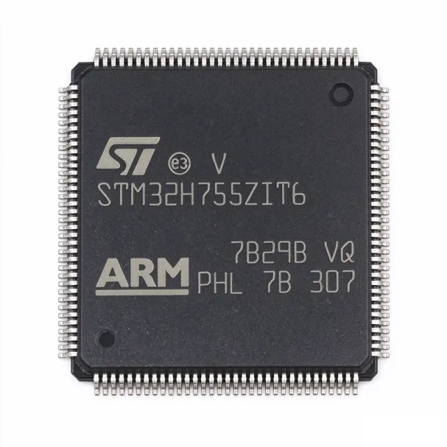
STM32H753ZIT6 - 480MHz Cortex-M7 MCU, 2MB Flash | STMicroelectronics
STM32H753ZIT6

STM32H753ZIT6 - 480MHz Cortex-M7 MCU, 2MB Flash | STMicroelectronics

The STMicroelectronics STM32H753ZIT6 is a high-performance 32-bit Arm Cortex-M7 microcontroller running at up to 480 MHz with 2 MB of dual-bank Flash and 1 MB of SRAM, housed in a 144-pin LQFP (20x20 mm, 0.5 mm pitch) package. It integrates a double-precision floating-point unit (FPU), a Chrom-ART Accelerator for 2D graphics, and a hardware cryptographic processor. A microcontroller (MCU) is a compact integrated circuit that combines a processor core, non-volatile program memory, volatile data memory, and programmable peripherals on a single die, allowing it to govern a dedicated embedded function without external support chips. The STM32H753ZIT6 sits at the top of the STM32H7 hierarchy: Cortex-M7 core -> STM32H7 series -> STM32 32-bit MCU family -> embedded microcontroller -> semiconductor. This position makes it the natural upgrade path from Cortex-M4/M3 designs that have run out of compute headroom. Key differentiators include the 480 MHz Cortex-M7 core with DSP and double-precision FPU instructions, 2 MB dual-bank Flash supporting read-while-write for live firmware updates, 1 MB SRAM, and a rich connectivity set: Ethernet MAC, USB OTG HS/FS, CAN FD, and multiple USART/SPI/I2C instances. A 16-bit ADC at 3.6 MSPS, a 12-bit DAC, and advanced motor-control timers round out the analog and control capability. Technically, the device is fabricated on a 40 nm process and operates from a 1.62 V to 3.6 V supply over -40 C to +85 C. An on-chip power management unit provides Sleep, Stop, and Standby modes for battery-powered designs, while the integrated LDO/SMPS regulator architecture differs from earlier STM32F7 designs that used a BYPASS_REG pin. Typical applications include industrial automation (PLCs, robotics), motor control (drives, pumps), medical devices (patient monitors, infusion pumps), and high-end audio equipment. The high clock speed and DSP instructions suit real-time signal processing, while the Chrom-ART Accelerator supports advanced graphical user interfaces. When designing with this MCU, decouple every VDD pin with a 100 nF capacitor placed close to the pin plus a 4.7 uF bulk capacitor, and feed VDDA through a ferrite bead from a dedicated analog supply. For Ethernet and USB HS, follow the STM32H7 reference manual (RM0433) layout guidance to preserve signal integrity. This page synthesizes distributor pricing, drop-in alternatives, and practical design notes not found in the manufacturer datasheet, giving engineers a single reference for selection, second-sourcing, and layout decisions.

USD $11,95 В наличии
STM32H755IIT6 - 480MHz Dual-Core MCU | STMicroelectronics
STM32H755IIT6

STM32H755IIT6 - 480MHz Dual-Core MCU | STMicroelectronics

The STMicroelectronics STM32H755IIT6 is a dual-core Arm Cortex-M7 and Cortex-M4 microcontroller with a Cortex-M7 operating up to 480 MHz, a Cortex-M4 operating up to 240 MHz, 2 MB of flash memory, and 1 MB of RAM in a 176-pin LQFP package measuring 24 x 24 mm. It combines high-performance signal processing, extensive connectivity, and integrated power-management functions in one microcontroller package. An STM32H7-series microcontroller is an embedded 32-bit Arm Cortex-M processor designed for industrial control, communications equipment, audio and digital signal processing, graphics, and high-complexity embedded systems. The STM32H755 architecture places a high-speed Cortex-M7 core and a Cortex-M4 core in one device, allowing firmware-intensive tasks to run concurrently with real-time control, communications, or signal-processing workloads. The STM32H755IIT6 provides 2 MB of flash for program storage and 1 MB of RAM for working memory. Its 46 communication and analog interfaces support a broad range of embedded connections, while its integrated SMPS and cryptographic capabilities reduce the need for additional support circuitry in suitable designs. The device supports 1.8 V, 2.5 V, and 3.3 V operating configurations according to the product listing. Dual-core operation is the principal architectural advantage. The 480 MHz Cortex-M7 core can handle demanding control loops, display processing, communications, or DSP workloads, while the 240 MHz Cortex-M4 core can execute independent real-time tasks. Software can use inter-core mechanisms supported by the STM32H7 platform to divide processing loads and reduce synchronization overhead compared with a single-core implementation. Typical applications include industrial automation and factory control, high-performance networking equipment, medical monitoring systems, motor and power-control platforms, professional audio equipment, and connected embedded products. The 176-LQFP package exposes substantially more I/O than small-package MCUs while remaining compatible with conventional leaded-board assembly processes. Board design should account for the STM32H7 family's demanding power, clocking, decoupling, and signal-integrity requirements. Follow the manufacturer datasheet's pin, voltage, decoupling, and external-component recommendations, and use ST's device configuration and pin-compatibility tools before changing an MCU on an existing PCB. This product summary consolidates the verified core, memory, package, interface, and sourcing information with practical application guidance and same-package STM32H7 replacement candidates. It also identifies which replacement claims require final pin, peripheral, firmware, and qualification review before production use.

Запрос цены Контакты
STM32H755ZIT6 - Dual-Core Cortex-M7/M4 MCU, 2MB Flash | STMicroelectronics
STM32H755ZIT6

STM32H755ZIT6 - Dual-Core Cortex-M7/M4 MCU, 2MB Flash | STMicroelectronics

The STMicroelectronics STM32H755ZIT6 is a high-performance dual-core 32-bit Arm microcontroller combining a Cortex-M7 core operating up to 480 MHz and a Cortex-M4 core up to 240 MHz, with 2 MB of dual-bank flash and 1 MB of SRAM in a 144-pin LQFP (20x20 mm) package. It targets industrial HMI, motor control, audio processing and edge-AI applications where heterogeneous compute partitioning between deterministic real-time control and high-throughput DSP/graphics is required. According to the STMicroelectronics product page, the STM32H755xI line integrates a Chrom-ART Accelerator, hardware crypto/hash accelerators, and a true random number generator. A microcontroller (MCU) is a compact integrated circuit that combines a processor core, on-chip memory (flash and SRAM), and programmable peripherals used to govern a specific operation in an embedded system. The STM32H755ZIT6 belongs to the STM32H7 family, which sits at the top of the ST Cortex-M portfolio between the mainstream STM32F4/F7 lines and the lower-power STM32L4/U5 lines. Its dual-core architecture enables one core to handle time-critical control while the other runs communication stacks, GUI rendering, or machine-learning inference, with shared access to peripherals through a bus-matrix arbitration scheme. Key differentiating features include the 480 MHz Cortex-M7 with double-precision FPU and L1 cache, the 240 MHz Cortex-M4 with single-precision FPU, 2 MB flash with read-while-write support, 1 MB SRAM split across DTCM, AXI SRAM and SRAM1/2/3 domains, and an integrated SMPS step-down converter for high-efficiency core supply. The device exposes 114 GPIO, 35 communication interfaces (including Ethernet, USB OTG HS/FS, CAN FD, SPI, I2C, UART, SDMMC), three 16-bit ADCs up to 3.6 MSPS, two 12-bit DACs, two SAI for audio, an LCD-TFT controller, a JPEG codec, and a crypto/hash suite compliant with AES, SHA and RSA. Built on a 40 nm low-power CMOS process, the part operates from 1.62 V to 3.6 V on VDD and supports an industrial -40 °C to +85 °C temperature range. The dual-bank flash with read-while-write capability simplifies in-field firmware upgrades and A/B partition schemes, while the Chrom-ART accelerator offloads 2D drawing to free the Cortex-M7 for application code. The integrated SMPS reduces core current draw by roughly 30% compared to an external LDO-only supply, easing thermal design in compact enclosures. Typical applications include industrial HMI panels with TFT LCD, motor-control inverter boards, smart-home gateways, audio DSP front-ends with SAI-to-DAC chains, vision-based edge-AI nodes using the JPEG codec, and medical instrumentation requiring deterministic USB or Ethernet connectivity. The dual-core topology is especially valuable when a real-time control loop must coexist with a Linux-like user interface stack on the same die. When designing with this device, treat the SMPS inductor selection as critical because ripple directly couples into the core logic rail. Provide a 4.7 µF input bulk plus 100 nF + 1 µF ceramic decoupling near each VDD pin, and follow the ST reference layout for the 240 MHz M7 traces to avoid signal-integrity issues. Boot pins BOOT0 and the option-byte bank must be configured before each power cycle, otherwise the part may revert to system memory bootloader. This page synthesizes distributor pricing, drop-in alternatives, and practical design notes not found on the ST product page alone.

USD $16,19 Контакты
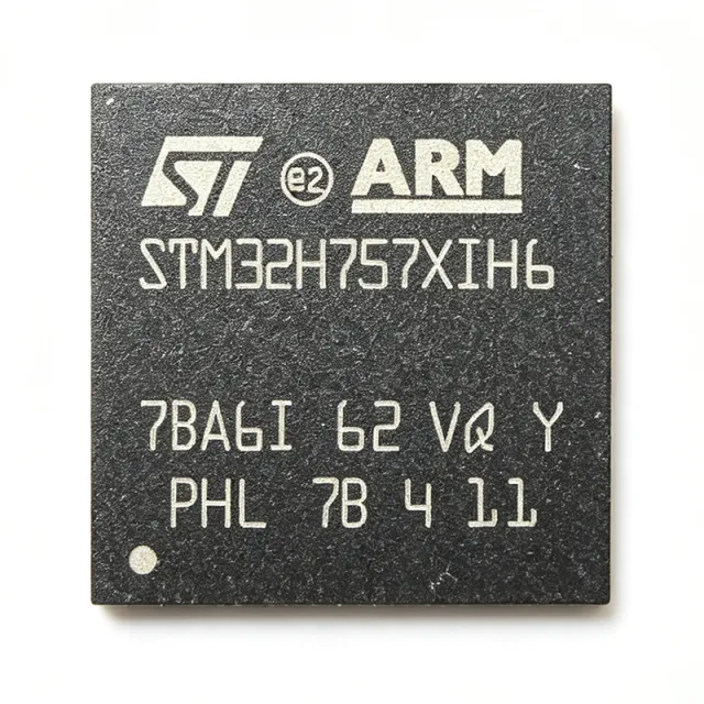
STM32H757XIH6 - Dual-Core M7/M4 MCU, 2MB Flash, TFBGA-240 | STMicroelectronics
STM32H757XIH6

STM32H757XIH6 - Dual-Core M7/M4 MCU, 2MB Flash, TFBGA-240 | STMicroelectronics

The STMicroelectronics STM32H757XIH6 is a high-performance dual-core microcontroller pairing an Arm Cortex-M7 core running up to 480 MHz with a Cortex-M4 core running up to 240 MHz, integrating 2 MB of flash and 1 MB of SRAM in a 240+25-ball TFBGA (14x14 mm) package. It belongs to the STM32H7 family, ST's flagship line of 32-bit microcontrollers designed for compute-intensive embedded workloads. A microcontroller (MCU) is a compact integrated circuit containing a processor core, on-chip memory (Flash and SRAM), and programmable peripherals, used to govern a specific function in an embedded system. The category spans from simple 8-bit controllers up to high-performance 32-bit dual-core devices like the STM32H7 series. Within ST's portfolio hierarchy, the STM32H7 sits above STM32F7, STM32L4, and STM32G4 families, targeting applications that require intensive computation, rich connectivity, and real-time responsiveness. Key features of the STM32H757XIH6 include the asymmetric dual-core architecture enabling workload partitioning between high-performance DSP/AI tasks (M7) and real-time control (M4), an integrated SMPS step-down converter for core supply efficiency, a hardware cryptographic accelerator with AES, hash, and true random number generator (TRNG), a Chrom-ART 2D graphics accelerator, an MIPI-DSI interface for displays, and 46 communication and analog interfaces including Ethernet, USB, CAN-FD, USART, SPI, I2C, multiple ADCs and DACs. The 1.62V to 3.6V supply range supports battery-backed operation. From a technical depth perspective, the device leverages ST's 40 nm low-power CMOS process, which enables the M7 core to sustain 480 MHz at Cortex-M7 performance levels with DSP extensions while keeping the M4 core running real-time tasks independently. The 2 MB dual-bank flash supports read-while-write operation, allowing one bank to execute code while the other is updated. A 16-stream DMA controller offloads data movement, and the flexible memory controller (FMC) extends the system with external SDRAM, NOR, or NAND flash. Typical applications include industrial PLC and HMI panels, motor-control drives (field-oriented control of PMSM and BLDC motors), high-end audio processors, medical patient monitoring, advanced driver-assistance systems (ADAS), robotics controllers, and smart-home/IoT edge gateways. The dual-core design is particularly suited to systems that must simultaneously run a graphical UI on the M7 and a deterministic control loop on the M4. When designing with the STM32H757XIH6, place 100 nF decoupling capacitors close to every VDD pin and use a bulk capacitor on the main 3.3 V rail. Boot-mode pins (BOOT0 and options bytes) must be configured correctly to select the desired boot source (Flash, system memory bootloader, or SDRAM). The TFBGA-240 package requires a 14x14 mm PCB land pattern with 0.8 mm ball pitch, and thermal copper area should be sized to keep junction temperature below 125 °C at full M7 load. This page synthesizes distributor pricing, drop-in TFBGA alternatives, and practical dual-core design notes not found in the manufacturer datasheet, giving engineers a single source for BOM decisions.

USD $12,18 Контакты
STM32H7A3RGT6 - 280MHz Cortex-M7 MCU with 1.4MB RAM | STMicroelectronics
STM32H7A3RGT6

STM32H7A3RGT6 - 280MHz Cortex-M7 MCU with 1.4MB RAM | STMicroelectronics

The STMicroelectronics STM32H7A3RGT6 is a high-performance 32-bit microcontroller based on the ARM Cortex-M7 core, operating at up to 280 MHz. It is part of the STM32H7A3 line, which is optimized for applications requiring high processing power, large memory, and advanced connectivity. The device is housed in a 64-pin LQFP package (LQFP64) and offers a rich set of peripherals, including multiple communication interfaces, analog-to-digital converters, and timers. A microcontroller (MCU) is a compact integrated circuit designed to govern a specific operation in an embedded system. It contains a processor core, memory (RAM and flash), and programmable input/output peripherals. The STM32H7A3RGT6 belongs to the STM32H7 family, which is part of the broader STM32 series of 32-bit microcontrollers. These MCUs are widely used in industrial control, consumer electronics, and IoT devices due to their balance of performance, power efficiency, and peripheral integration. Key features of the STM32H7A3RGT6 include a 280 MHz ARM Cortex-M7 core with double-precision floating-point unit (FPU), 1.4 MB of SRAM, and 2 MB of flash memory. It supports external memory interfaces for SDRAM, SRAM, and NOR flash, and includes a Chrom-ART Accelerator for graphics. The device also features a comprehensive set of security features, including hardware cryptographic acceleration and a true random number generator (TRNG). The STM32H7A3RGT6 is built on a high-performance architecture that includes a 32-bit multi-AHB bus matrix, enabling efficient data transfer between the core, memory, and peripherals. The Cortex-M7 core with its 6-stage pipeline and branch prediction delivers high instruction throughput, making it suitable for real-time control and digital signal processing applications. The device also includes a memory protection unit (MPU) and a cache for both instruction and data, enhancing system reliability and performance. Typical applications include industrial automation, motor control, smart home devices, and high-end consumer electronics. The large memory and high clock speed make it ideal for applications requiring complex algorithms, such as predictive maintenance and advanced user interfaces. The device's rich connectivity options, including Ethernet, USB, and multiple UART/SPI/I2C interfaces, enable seamless integration into networked systems. When designing with the STM32H7A3RGT6, ensure proper power supply decoupling with 100 nF capacitors close to each power pin and a 4.7 uF bulk capacitor. The device supports a wide supply voltage range of 1.62V to 3.6V, allowing flexible power design. For high-speed interfaces, follow the layout guidelines in the datasheet to maintain signal integrity.

Запрос цены Контакты
STM32H7A3RIT6 - 280MHz Cortex-M7 MCU, 2MB Flash | STMicroelectronics
STM32H7A3RIT6

STM32H7A3RIT6 - 280MHz Cortex-M7 MCU, 2MB Flash | STMicroelectronics

The STMicroelectronics STM32H7A3RIT6 is a high-performance ARM Cortex-M7 32-bit RISC-core microcontroller operating at up to 280 MHz, integrating 2 MB of Flash memory and 1376 KB of SRAM in a 64-pin LQFP (10x10 mm) package. The device is built on a 40 nm CMOS process and includes a double-precision FPU, L1 cache (16 KB +16 KB), and DSP instructions, delivering up to 1177 DMIPS / 2741 CoreMark performance for compute-intensive embedded workloads. A microcontroller (MCU) is a single-chip computer that integrates a CPU core, memory, and programmable peripherals; the STM32 family is the 32-bit ARM Cortex-M based MCU portfolio from STMicroelectronics, spanning ultra-low-power (L0/L4), mainstream (F0/F1/F3/G0/G4), high-performance (F4/F7/H7), and wireless (WB/WL) lines. The Cortex-M7 core sits at the top of the Cortex-M performance hierarchy, above Cortex-M4/M33, and the H7A3 line further extends the H7 family with larger Flash and a cost-optimized peripheral set. Key features of the STM32H7A3RIT6 include 2 MB single-bank Flash with ECC, 1376 KB total SRAM (1 MB DTCM + 192 KB SRAM1 + 64 KB SRAM2 + 64 KB SRAM3 + 56 KB SRAM4), extensive connectivity (USB 2.0 FS+OTG, CAN-FD x2, SDMMC x2, USART/UART/SPI/I2C), a 16-bit ADC, two 12-bit DACs, two 32-bit timers, and multiple 16-bit timers. An external memory interface (FMC) and OCTOSPI/Quad-SPI interface allow expansion to external Flash/PSRAM, supporting displays up to XGA resolution. Typical applications include industrial motor control and factory automation, human-machine interfaces (HMI) with TFT LCD, audio processing with the dedicated SAI interface, IoT gateways, drones/flight controllers, point-of-sale terminals, and high-performance consumer devices. Designers often select the H7A3 line for higher performance than F7/F4 with no need for the dual-core A7 architecture of the H7 family. When designing with this MCU, ensure the SMPS or external LDO supplies 1.62-3.6 V to VDD with correct power sequencing; D1 and D2 power domains require separate decoupling. Use ST's STM32CubeMX for clock tree, peripheral pinout, and code generation to minimize bring-up time.

Запрос цены Контакты
STM32H7A3VGT6 - 280MHz Cortex-M7 MCU, 1MB Flash | STMicroelectronics
STM32H7A3VGT6

STM32H7A3VGT6 - 280MHz Cortex-M7 MCU, 1MB Flash | STMicroelectronics

The STMicroelectronics STM32H7A3VGT6 is a high-performance Arm Cortex-M7 based microcontroller operating at up to 280 MHz, delivering 1.4 MB of flash memory and 1.4 MB of SRAM in a 100-pin LQFP package. It is part of the STM32H7A3 line, designed for applications requiring intensive computation, rich connectivity, and advanced security features. What is a microcontroller (MCU)? A microcontroller is a compact integrated circuit that combines a processor core, memory, and programmable input/output peripherals on a single chip. It is the brain of embedded systems, executing firmware to control devices, process sensor data, and communicate with other systems. MCUs are classified within the broader hierarchy of embedded processors, which includes microprocessors, digital signal processors (DSPs), and system-on-chips (SoCs). The STM32H7A3VGT6 sits at the high-performance end of the MCU spectrum, offering near-DSP-level compute capability. Key features include a 280 MHz Arm Cortex-M7 core with double-precision FPU, 1.4 MB flash, 1.4 MB SRAM, and a rich set of peripherals: multiple 16-bit and 32-bit timers, 12-bit ADCs, 12-bit DACs, and advanced communication interfaces (USART, SPI, I2C, FDCAN, USB OTG, Ethernet MAC). The device also integrates a hardware cryptographic accelerator (AES, DES, 3DES, SHA-1, SHA-256) and a true random number generator (TRNG) for secure applications. Technically, the STM32H7A3VGT6 is built on a 40nm process, enabling high clock speeds with moderate power consumption. The Cortex-M7 core features a 6-stage pipeline, branch prediction, and a memory protection unit (MPU), supporting real-time deterministic execution. The device supports external memory interfaces (FMC) for SDRAM, NOR, and NAND flash expansion, and a flexible memory controller for parallel and serial interfaces. Typical applications include industrial automation (PLC, motor control), medical devices (patient monitors, infusion pumps), consumer electronics (smart speakers, wearables), and IoT gateways. The high core speed and rich peripherals make it suitable for real-time control, audio processing, and edge AI inference. When designing with this device, ensure adequate decoupling on all power pins and a proper crystal oscillator layout for the HSE. The 100-pin LQFP package requires careful thermal management; use a 4-layer PCB with a solid ground plane to dissipate heat effectively.

Запрос цены Контакты
STM32H7A3VIT6 - 280MHz Cortex-M7 MCU, 2MB Flash, LQFP-100 | STMicroelectronics
STM32H7A3VIT6

STM32H7A3VIT6 - 280MHz Cortex-M7 MCU, 2MB Flash, LQFP-100 | STMicroelectronics

The STMicroelectronics STM32H7A3VIT6 is a high-performance 32-bit ARM Cortex-M7 microcontroller operating at up to 280 MHz, delivering 2 MB of Flash memory and approximately 1.4 MB of SRAM in a 100-pin LQFP (14x14 mm) package. It belongs to the STM32H7A3xI/G line that combines a single-core Cortex-M7 with a rich set of peripherals aimed at motor control, audio, graphics and general-purpose high-speed embedded designs. A microcontroller (MCU) is a single-chip computer that integrates a CPU core, non-volatile program memory (Flash), volatile working memory (SRAM), and a wide range of peripheral interfaces into one package. Within the broader semiconductor taxonomy, an MCU sits under microcontrollers, which are a subcategory of integrated circuits (ICs); the Cortex-M7 core specifically belongs to the ARM Cortex-M family of embedded cores, optimized for deterministic real-time performance and DSP workloads. The STM32H7 series extends this family with the highest clock rates and largest memory footprints in the STM32 portfolio. Key features include a 16-bit ADCs sampling up to 3.6 MSPS, fast 12-bit DACs, two USB 2.0 Full-Speed/High-Speed OTG controllers, multiple CAN FD, SDMMC, FMC, and a TFT-LCD controller. On-chip math accelerators (FMAC, CORDIC) and the Chrom-ART (DMA2D) graphics engine offload CPU-intensive operations, while hardware cryptographic accelerators and a true random number generator (TRNG) support secure connectivity use cases. The Cortex-M7 core includes a double-precision FPU, L1 instruction and data caches (16 KB each), and a tightly-coupled SRAM region for zero-wait-state execution, enabling 280 MHz operation with sustained DSP throughput. The bus matrix is multi-layer AHB, allowing concurrent high-bandwidth access between the CPU, the Chrom-ART engine, and the SDMMC/USB peripherals without bus starvation. Typical applications include industrial motor drives, factory automation PLCs, audio processing and professional audio interfaces, HMI panels with TFT displays, IoT edge nodes with secure connectivity, and automotive-grade body and comfort modules (when ordered in the AEC-Q100 'Q' suffix variant). When designing with the STM32H7A3VIT6, pay close attention to power-supply decoupling and trace impedance around the high-speed SDMMC and USB signals. Proper boot-mode configuration on the BOOT0 pin and OTP area management is essential for field-deployable firmware security. This page synthesizes distributor pricing, pin-compatible drop-in alternatives, and practical design notes that are not found in the manufacturer datasheet alone.

Запрос цены Контакты
STM32H7A3ZIT6 - 280MHz Cortex-M7 2MB MCU | STMicroelectronics
STM32H7A3ZIT6

STM32H7A3ZIT6 - 280MHz Cortex-M7 2MB MCU | STMicroelectronics

STMicroelectronics STM32H7A3ZIT6 is a high-performance 32-bit Arm Cortex-M7 microcontroller operating at up to 280 MHz, with 2 MB of Flash memory, 1.4 MB of RAM, and a 144-pin LQFP package measuring 20 mm by 20 mm. The device combines high-throughput digital control with extensive analog and communication peripherals for industrial, communications, audio, and embedded-processing systems. An Arm Cortex-M7 microcontroller is a 32-bit reduced-instruction-computing core integrated with memory, peripherals, and communication interfaces on one semiconductor device. The STM32H7 family hierarchy includes the Cortex-M7 core, high-performance STM32H7 microcontrollers, 32-bit embedded MCUs, and the broader semiconductor category. Compared with simpler Cortex-M devices, the Cortex-M7 architecture supports higher processing throughput and more demanding real-time workloads while retaining a highly integrated embedded-control form factor. The STM32H7A3ZIT6 provides 2 MB of Flash, 1.4 MB of RAM, and operation at up to 280 MHz according to the manufacturer datasheet. Its device family also includes an SMPS and a broad selection of communication and analog interfaces. The 144-LQFP package exposes enough I/O for external memory, sensors, communications, and mixed-signal equipment without requiring a very fine-pitch BGA layout. This makes the controller suitable for designs that need substantial processing performance and peripheral access while retaining board-level routing simplicity. The STM32H7A3 family is designed for high-performance embedded control, combining a fast Cortex-M7 core with flexible memory resources and extensive serial peripherals. Depending on the selected family configuration, these devices support interfaces suited to Ethernet-class networking, USB connectivity, industrial serial links, audio processing, and external data acquisition. The manufacturer's STM32Cube development environment and associated ecosystem support peripheral configuration, code generation, debugging, and board bring-up. Typical applications include industrial automation controllers, networked data-acquisition equipment, communications gateways, audio and DSP systems, medical monitoring equipment, and high-performance embedded user interfaces. The 2 MB Flash capacity supports larger firmware and application code, while the 1.4 MB RAM can accommodate data buffers, graphics acceleration workflows, and real-time signal processing. The 144-pin package is especially useful when a design requires numerous discrete I/O functions or several external serial interfaces. A critical implementation consideration is power and signal integrity. Place all required decoupling capacitors close to their corresponding supply pins, preserve the recommended high-speed layout, and use the pin-description table in the manufacturer datasheet when assigning tracks. Differential interfaces, clocks, and analog inputs also require controlled return paths and appropriately sized ground-plane geometry to prevent the MCU's high-speed activity from degrading measurement accuracy or peripheral performance. This page combines the STM32H7A3ZIT6 electrical and packaging details, sourcing information, verified drop-in alternatives, application guidance, and PCB design notes into one engineering-focused reference. It also highlights where pin-compatible alternatives differ in memory, temperature grade, qualification, or peripheral capability, helping designers choose the appropriate MCU without confusing footprint compatibility with complete functional equivalence.

Запрос цены Контакты
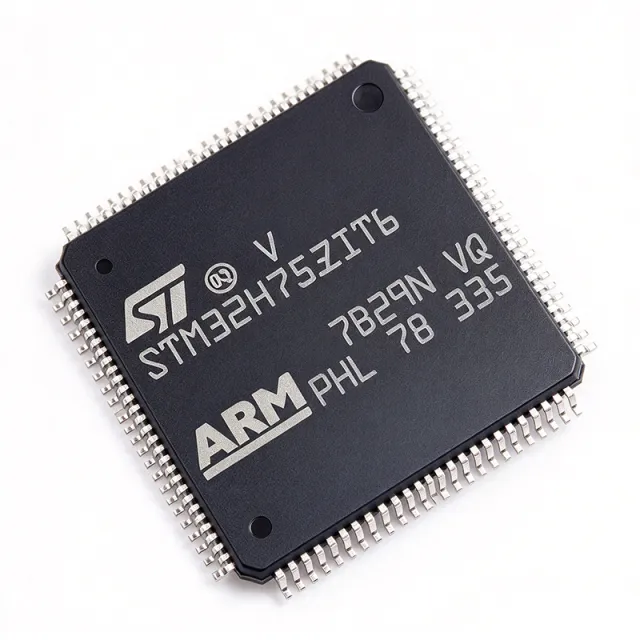
STM32H7A3ZIT6Q - Cortex-M7 MCU 280MHz 2MB Flash | STMicroelectronics
STM32H7A3ZIT6Q

STM32H7A3ZIT6Q - Cortex-M7 MCU 280MHz 2MB Flash | STMicroelectronics

The STMicroelectronics STM32H7A3ZIT6Q is a high-performance 32-bit ARM Cortex-M7 microcontroller operating at up to 280 MHz, featuring 2 MB of Flash and approximately 1376 KB of SRAM, housed in a 144-pin LQFP (20x20 mm) package. The 'Q' suffix indicates the industrial-grade temperature range and ST's automotive-grade qualification per AEC-Q100, making it suitable for harsh-environment applications that demand both processing throughput and long-term reliability. What is an ARM Cortex-M7 microcontroller? It is a 32-bit RISC processor core designed by Arm for embedded real-time workloads. The Cortex-M7 superset within the Cortex-M family introduces a six-stage superscalar pipeline, dual-issue capability, single/double-precision FPU, DSP extensions, and an instruction cache (I-cache) plus data cache (D-cache) with optional TCM (Tightly Coupled Memory) interfaces. In the broader taxonomy it sits above Cortex-M4 (no cache, no dual-issue) and below Cortex-A application processors, occupying the high-performance MCU tier. Key features of the STM32H7A3ZIT6Q include the Cortex-M7 core with double-precision FPU and L1 cache (16 KB I-cache + 16 KB D-cache), Chrom-ART graphics accelerator for TFT-LCD pipelines, up to 1.4 MB contiguous SRAM with multiple block options, two 16-bit ADCs (up to 3.6 MSPS), two 12-bit DACs, multiple U(S)ART/SPI/I2C/FDCAN/USB interfaces, SDMMC, Ethernet MAC, and a JTAG/SWD debug interface. The device integrates a 32-bit timer, 16-bit timers, and an HRTIM high-resolution timer for power-conversion control. Architecturally, the H7A3 line leverages ST's 40 nm embedded-Flash process, with bus-matrix decoupling of code (TCM), main SRAM, and peripherals for deterministic interrupt latency. The dual-bank Flash supports read-while-write, allowing firmware updates without halting execution. Cryptography acceleration (AES, SHA, RNG) is included for secure-boot and TLS workloads. Typical applications include industrial motor control (field-oriented control of PMSM and induction motors via HRTIM), HMI panels with TFT-LCD rendered through Chrom-ART, building-automation controllers, solar inverters, EV charging station control boards, and audio DSP front-ends. The wide temperature range and AEC-Q100 grade extend fit to chassis ECUs and body controllers. Design consideration: at 280 MHz the device dissipates roughly 250-400 mW depending on peripheral activity; a four-layer PCB with a continuous ground plane beneath the LQFP exposed pad is recommended to keep junction temperature within the 125 C industrial limit. Use ST's STM32CubeMX to generate pin-multiplexing tables and the HAL/LOWER-LAYER driver scaffolding. This page synthesizes distributor pricing, drop-in same-package alternatives, and AEC-Q100 design notes not found on the standalone manufacturer datasheet.

Запрос цены Контакты
STM32H7B0RBT6 - 32-bit Arm Cortex-M7 MCU 280MHz | STMicroelectronics
STM32H7B0RBT6

STM32H7B0RBT6 - 32-bit Arm Cortex-M7 MCU 280MHz | STMicroelectronics

The STMicroelectronics STM32H7B0RBT6 is a high-performance 32-bit microcontroller based on the Arm Cortex-M7 core, operating at up to 280 MHz. It is part of the STM32H7 series, designed for demanding applications requiring high processing power, advanced connectivity, and rich analog peripherals. The device is housed in a 64-pin LQFP package (LQFP64) and provides a comprehensive set of features including 128 Kbytes of Flash memory, 1 Mbyte of RAM, and a wide range of communication interfaces. What is a microcontroller? A microcontroller (MCU) is a compact integrated circuit designed to govern a specific operation in an embedded system. It contains a processor core, memory (Flash and RAM), and programmable input/output peripherals on a single chip. Microcontrollers are the brains of countless electronic devices, from automotive engine control units to IoT sensors and industrial automation systems. The STM32H7 series represents the high-performance tier of STMicroelectronics' STM32 portfolio, offering the Arm Cortex-M7 core with double-precision floating-point unit (FPU) and DSP instructions, making it suitable for real-time control, signal processing, and AI at the edge. Key features of the STM32H7B0RBT6 include a 280 MHz Arm Cortex-M7 core with 128 Kbytes of Flash and 1 Mbyte of RAM, a 16-bit ADC with up to 3.6 MSPS, multiple 16-bit and 32-bit timers, and a rich set of communication interfaces including USART, SPI, I2C, CAN, USB OTG, and Ethernet. The device also features a Chrom-ART Accelerator for 2D graphics, a cryptographic acceleration unit, and a true random number generator (TRNG). These features enable high-performance computing and secure data handling in a compact footprint. From a technical depth perspective, the STM32H7B0RBT6 leverages a 32-bit Arm Cortex-M7 core with a 6-stage pipeline, branch prediction, and a memory protection unit (MPU). The core supports single-cycle multiply-accumulate (MAC) instructions and hardware divide, enhancing real-time performance. The device integrates a flexible memory controller (FMC) for external memory expansion, and a power management unit with multiple low-power modes, including Sleep, Stop, and Standby, to optimize energy consumption. The advanced analog peripherals, including a 16-bit ADC with oversampling and a 12-bit DAC, provide high-resolution data acquisition for industrial and medical applications. Typical applications for the STM32H7B0RBT6 include industrial motor control, power conversion, advanced human-machine interfaces (HMI), IoT gateways, audio processing, and medical devices. Its high clock speed and rich peripheral set make it ideal for applications requiring real-time control and complex algorithms, such as robotics and drone flight controllers. The device's connectivity options, including Ethernet and USB, enable seamless integration into networked systems. When designing with the STM32H7B0RBT6, ensure adequate decoupling of the power supply pins with 100 nF capacitors placed close to each VDD pin, and a 4.7 uF bulk capacitor. The VDDA pin requires a dedicated 1 uF capacitor to ground for analog performance. For high-speed communication interfaces, pay attention to PCB layout to minimize signal integrity issues. The device supports a wide supply voltage range of 1.62V to 3.6V, allowing flexible power design.

Запрос цены Контакты
STM32H7B0VBT6 - 280MHz Cortex-M7 MCU, 128KB Flash | STMicroelectronics
STM32H7B0VBT6

STM32H7B0VBT6 - 280MHz Cortex-M7 MCU, 128KB Flash | STMicroelectronics

The STMicroelectronics STM32H7B0VBT6 is a high-performance 32-bit microcontroller based on the ARM Cortex-M7 core, operating at up to 280 MHz. It is part of the STM32H7 series, designed for demanding applications requiring high processing power, advanced connectivity, and rich analog peripherals. The device is housed in a 100-pin LQFP package (VBT6 suffix) and provides a balanced feature set for industrial, consumer, and IoT applications. A microcontroller (MCU) is a compact integrated circuit designed to govern a specific operation in an embedded system. It contains a processor core, memory, and programmable input/output peripherals on a single chip. The STM32H7B0VBT6 belongs to the high-performance MCU category, positioned above mainstream MCUs like the STM32F4 series, and is part of the broader STM32 family from STMicroelectronics. Its Cortex-M7 core with double-precision FPU and DSP instructions enables efficient handling of complex algorithms, making it suitable for real-time control, signal processing, and AI edge applications. Key features include a 280 MHz ARM Cortex-M7 core with double-precision FPU, 128 KB of flash memory, and 1.4 MB of SRAM. The device supports external memory interfaces via FMC and OCTOSPI, enabling expansion of code and data storage. It integrates a rich set of peripherals including multiple 16-bit and 32-bit timers, 12-bit ADCs, DACs, and advanced communication interfaces such as USART, SPI, I2C, CAN FD, USB OTG, and Ethernet. The device operates from a 1.62V to 3.6V supply and is available in a 100-pin LQFP package with a temperature range of -40°C to +85°C. The STM32H7B0VBT6 is built on a high-performance architecture with a 32-bit multi-AHB bus matrix, enabling concurrent access to memory and peripherals. It includes a Chrom-ART Accelerator for 2D graphics, a cryptographic acceleration unit, and a true random number generator. The device supports various low-power modes, including Sleep, Stop, and Standby, with typical power consumption in the microamp range in standby mode. The advanced memory protection unit (MPU) and secure access modes enhance system security. Typical applications include industrial control systems, motor control, smart home gateways, audio processing, and high-end consumer electronics. The high clock speed and rich peripherals make it ideal for real-time control and edge AI inference. The device also supports external memory expansion, making it suitable for applications requiring large data buffers or code storage. When designing with this MCU, ensure proper decoupling of the power supply pins with 100nF capacitors placed close to each VDD pin. The VDDA pin requires a dedicated 1uF capacitor for analog performance. For high-speed communication interfaces, pay attention to PCB layout to minimize signal integrity issues. The device supports in-circuit programming and debugging via SWD and JTAG interfaces, facilitating development.

Запрос цены Контакты
STM32H7B3ZIT6 - 280MHz Cortex-M7 MCU, 2MB Flash | STMicroelectronics
STM32H7B3ZIT6

STM32H7B3ZIT6 - 280MHz Cortex-M7 MCU, 2MB Flash | STMicroelectronics

The STMicroelectronics STM32H7B3ZIT6 is a high-performance 32-bit microcontroller based on the Arm Cortex-M7 core, operating at up to 280 MHz. It integrates 2 MB of flash memory and 1.4 MB of SRAM, making it suitable for demanding applications such as industrial control, motor control, and high-end consumer electronics. The device is housed in a 144-pin LQFP package (LQFP144) with a 20x20 mm body, providing ample I/O for complex system integration. A microcontroller (MCU) is a compact integrated circuit designed to govern a specific operation in an embedded system. It contains a processor core, memory, and programmable input/output peripherals. The STM32H7B3ZIT6 belongs to the STM32H7 series, which is part of the broader STM32 family of 32-bit flash microcontrollers. This family is widely used in embedded systems, ranging from simple sensor nodes to complex industrial automation, due to its balance of performance, power efficiency, and peripheral integration. Key features of the STM32H7B3ZIT6 include a 280 MHz Cortex-M7 core with double-precision FPU, a Chrom-ART Accelerator for 2D graphics, and a comprehensive set of communication interfaces including Ethernet, USB OTG HS, and multiple USARTs/SPIs/I2Cs. It also features a 16-bit ADC with 3.6 MSPS, a cryptographic acceleration unit, and a true random number generator. The device supports a wide supply voltage range of 1.62V to 3.6V and operates over a temperature range of -40°C to +85°C. Architecturally, the STM32H7B3ZIT6 leverages a dual-core architecture in some variants, but this specific model features a single Cortex-M7 core with an L1 cache, achieving 856 CoreMark score. The device includes a flexible memory controller supporting external SDRAM, SRAM, and NOR/NAND flash, enabling large data buffers and graphics frame buffers. The Chrom-ART Accelerator offloads 2D drawing tasks from the CPU, improving graphics performance in HMI applications. Typical applications include high-end human-machine interfaces (HMI), industrial automation controllers, motor control drives, and audio processing. The high clock speed and rich peripherals make it ideal for real-time control and signal processing. The device also supports secure boot and firmware update mechanisms, enhancing system security. When designing with this MCU, ensure adequate decoupling on all power pins and a stable clock source. The internal LDO can be bypassed for lower power consumption, but careful attention to the power sequencing is required. The device offers multiple low-power modes, allowing optimization for battery-powered applications.

Запрос цены Контакты
STM32L010C6T6 - Ultra-Low-Power ARM Cortex-M0+ MCU | STMicroelectronics
STM32L010C6T6

STM32L010C6T6 - Ultra-Low-Power ARM Cortex-M0+ MCU | STMicroelectronics

The STMicroelectronics STM32L010C6T6 is an ultra-low-power 32-bit microcontroller based on the ARM Cortex-M0+ core, operating at up to 32 MHz. It is part of the STM32L0 series, designed for energy-efficient applications requiring long battery life. The device features 32 KB of Flash memory and 8 KB of SRAM, with a wide supply voltage range of 1.8V to 3.6V, making it suitable for battery-powered and energy-harvesting systems. An ultra-low-power microcontroller (MCU) is a system-on-chip that integrates a processor core, memory, and peripherals, optimized to minimize power consumption while maintaining performance. The STM32L010C6T6 belongs to the STM32L0 family, which is part of the broader STM32 32-bit MCU portfolio. This hierarchy places it within the ARM Cortex-M0+ processor category, a 32-bit RISC architecture known for its energy efficiency and simplicity, ideal for cost-sensitive and power-constrained applications. Key features include multiple low-power modes (Sleep, Low-power Run, Low-power Sleep, Stop, Standby) with current consumption as low as 0.29 µA in Standby mode with RTC, and 3.4 µA in Stop mode. The MCU integrates a 12-bit ADC with up to 16 channels, two comparators, a DMA controller, and a variety of communication interfaces including I2C, SPI, and USART. It also includes a real-time clock (RTC) with calendar and alarm functions, and a true random number generator (RNG). The STM32L010C6T6 is built on ST's ultra-low-power technology, featuring a flexible clock management with an internal 16 MHz RC oscillator and an external 32.768 kHz crystal for the RTC. The device supports a wide operating temperature range of -40°C to +85°C, and is available in a 48-pin LQFP package (7x7 mm). It is RoHS compliant and lead-free, meeting environmental standards for global distribution. Typical applications include battery management systems, portable medical devices, smart sensors, IoT nodes, and industrial control systems. Its low power consumption and rich analog peripherals make it ideal for applications requiring precise analog measurements and long operational life. When designing with this MCU, careful attention should be paid to power supply decoupling and PCB layout to minimize noise and ensure reliable operation. The use of the internal RC oscillator can reduce external component count, but for time-critical applications, an external crystal is recommended for better accuracy.

Запрос цены Контакты
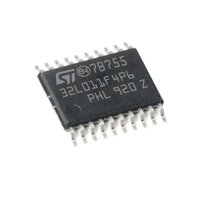
STM32L010F4P6 - 32MHz Cortex-M0+ 16KB MCU | STMicroelectronics
STM32L010F4P6

STM32L010F4P6 - 32MHz Cortex-M0+ 16KB MCU | STMicroelectronics

The STMicroelectronics STM32L010F4P6 is an ultra-low-power 32-bit microcontroller with an Arm Cortex-M0+ core operating at 32 MHz, 16 KB of embedded Flash memory, 2 KB of SRAM, and a 20-pin TSSOP package. The device is designed for compact, low-cost embedded systems that require efficient control, analog measurement, and low-power operation. A microcontroller is a programmable integrated circuit that combines a processor core, nonvolatile program memory, volatile data memory, and peripherals on one semiconductor die. The STM32L0 family belongs to the broader hierarchy of embedded processors, 32-bit RISC microcontrollers, and energy-efficient embedded systems. Its Cortex-M0+ architecture provides a compact instruction set suitable for real-time control, while integrated timers, ADC, RTC, and watchdogs reduce the need for external components. Key features include a 12-bit analog-to-digital converter with hardware oversampling, two general-purpose 16-bit timers, one low-power timer, one real-time clock, and SysTick. The device also includes two watchdog mechanisms: an independent watchdog with window capability and a window watchdog based on the bus clock. These resources support periodic sensing, reliable timekeeping, motor or actuator control, and autonomous low-power operation in a single 20-pin TSSOP device. The STM32L010F4P6 uses the Arm Cortex-M0+ 32-bit RISC core and operates at a maximum frequency of 32 MHz. Its 16 KB Flash memory provides sufficient space for compact applications, while the 2 KB SRAM supports working variables, stack space, and modest real-time data processing. The 12-bit ADC with hardware oversampling improves effective input-signal resolution and can reduce the demands placed on an external measurement front end when the firmware performs appropriate averaging and calibration. Typical applications include compact sensor nodes, building controls, appliance interfaces, battery-powered instruments, industrial monitoring modules, and low-cost motor-control products. The separate low-power timer and RTC are especially useful when a product must preserve timing information or wake periodically from a low-energy operating state. Its small package also supports designs where board area is constrained. When laying out the PCB, use the manufacturer pin-description and package-outline information to assign power, ground, reset, debug, clock, and GPIO functions. Place decoupling capacitors close to the supply pins, keep the NRST path free of disruptive switching nodes, and route the SWD programming signals consistently with the package pinout. Firmware should also configure unused pins deliberately to avoid unnecessary current consumption. This product page combines the official STM32L010F4/K4 datasheet information, manufacturer product-page details, and engineering guidance focused on memory sizing, peripheral use, low-power behavior, pin assignment, and practical replacement decisions for compact STM32L0 designs.

Запрос цены Контакты
STM32L010K4T6 - 32MHz Cortex-M0+ MCU 16KB | STMicroelectronics
STM32L010K4T6

STM32L010K4T6 - 32MHz Cortex-M0+ MCU 16KB | STMicroelectronics

The STMicroelectronics STM32L010K4T6 is an ultra-low-power value-line 32-bit ARM Cortex-M0+ microcontroller integrating 16 KB of Flash, 2 KB of SRAM, and 128 bytes of user EEPROM in a 32-pin LQFP 7x7 mm package. The device operates up to 32 MHz from a 1.65 V to 3.6 V supply and includes a 12-bit ADC, two general-purpose 16-bit timers, one low-power timer (LPTIM), one RTC, SysTick, two watchdogs (independent and window), and standard STM32 communication peripherals such as I2C, SPI, and USART. What is an ultra-low-power microcontroller? An ultra-low-power MCU (often called ULP MCU) is a microcontroller architected around deep sleep modes in which most analog and digital peripherals are gated off, the CPU is stopped, and current consumption can drop to the nanoampere range. These parts target battery-powered and energy-harvesting designs where the average sleep current, not the active current, dominates battery life. The STM32L010 sits at the entry level of the STM32L0 family, descending from STMicroelectronics' broader STM32 32-bit MCU family that also includes mainstream (F0/F1/F3), high-performance (F4/F7/H7), and wireless (WB/WL) lines. Key features that differentiate the K4 from siblings in the L0 line include the inclusion of 128 bytes of true EEPROM (rare for STM32 and useful for storing calibration or user settings without page-erase wear on Flash), 4 KB of usable SRAM after bootloader reservation, an extended temperature range of -40 C to +85 C, and four low-power modes (Sleep, Low-power sleep, Stop with RTC, and Standby). The integrated 12-bit ADC supports hardware oversampling, enabling up to 16-bit equivalent resolution for sensor measurements in slow-moving signals such as temperature, light, or battery voltage. At the architectural level, the Cortex-M0+ core uses the Thumb-2 instruction subset optimized for code density, single-cycle I/O via the ARMv6-M architecture, and a Nested Vectored Interrupt Controller (NVIC). The part is supplied in a 32-pin LQFP package (7x7 mm body) which keeps the PCB footprint compact while leaving enough GPIO for typical embedded designs. The K4 suffix maps to a 32-pin LQFP package; the F4 variant ships the same die in a 20-pin TSSOP for tighter boards. Typical applications include battery-powered IoT sensor nodes, smart meters, wearables, remote controls, and any ultra-low-power embedded design that needs true 32-bit performance with sub-microamp standby. The compact 32-pin LQFP footprint and ST-supplied ecosystem (CubeMX, HAL, STM32CubeIDE, and the X-CUBE-ULP Expansion Package) reduce time to prototype. When designing with this part, pay attention to the stop-mode current budget and decoupling. Two 100 nF ceramic caps must be placed within 2 mm of VDD/VDDA, plus a 1 uF bulk cap on the regulator input; the NRST pin requires a 10 kohm pull-up and a 100 nF cap for a reliable reset, and the BOOT0 pin must be tied low for normal Flash boot. Estimated power-down current in Standby with RTC running is typically under 1 uA, allowing coin-cell designs to last years. This page synthesizes distributor pricing, drop-in alternatives within the same 32-pin LQFP footprint, and practical design notes not assembled in the ST datasheet alone.

Запрос цены Контакты
STM32L010K8T6 - 32MHz Cortex-M0+ 64KB MCU | STMicroelectronics
STM32L010K8T6

STM32L010K8T6 - 32MHz Cortex-M0+ 64KB MCU | STMicroelectronics

STMicroelectronics STM32L010K8T6 is an ultra-low-power 32-bit Arm Cortex-M0+ microcontroller rated at 32 MHz, with 64 KB of Flash memory, 8 KB of SRAM, and 256 bytes of EEPROM in a 32-LQFP 7 x 7 mm package. It combines a compact RISC core with a 12-bit ADC, multiple timers, an RTC, and two watchdog mechanisms for embedded control designs. A microcontroller is a programmable semiconductor that integrates a processor core, memory, and peripherals into one device. Within the embedded-control hierarchy, this part belongs to the STM32L0 value-line family of low-power MCUs and belongs to the broader Arm Cortex-M microcontroller ecosystem. Its small LQFP package supports compact PCB layouts while retaining individually accessible pins for prototyping, inspection, and mixed-signal designs. The STM32L010K8T6 provides a 12-bit ADC with hardware oversampling, two general-purpose 16-bit timers, one low-power timer, one real-time clock, and SysTick capability. Independent-clock and window watchdog functions add monitoring and recovery options for embedded systems. Its 64 KB Flash supports firmware and application code, while 8 KB SRAM accommodates working data and stack operations without requiring external memory in compact designs. The Arm Cortex-M0+ architecture uses a 32-bit RISC instruction set and operates up to 32 MHz. This combination is appropriate for control tasks that need predictable embedded processing without a high-performance application processor. The STM32L010K8/R8 family also includes several analog features, allowing a design to combine digital control, sensor acquisition, timing, and low-power peripheral management in one device. Typical uses include battery-powered sensor nodes, compact industrial controllers, building-access peripherals, low-power monitoring equipment, motor-control helpers, and small instrument-control systems. The ADC supports analog measurement, while the timers and RTC support periodic sampling, timekeeping, and event handling. For designs needing more communications or processing, the family can be paired with dedicated interface transceivers and power-management components. The principal design consideration is that this MCU is a general-purpose embedded controller rather than a high-pin-count system processor. Confirm the complete LQFP-32 pin assignment, peripheral alternate functions, and application-specific timing requirements in the manufacturer datasheet before final routing. Place decoupling capacitors close to the supply pins and assign unused pins according to the device recommendations in that datasheet. This page combines manufacturer specifications, package and pin information, sourcing guidance, application patterns, and a same-package replacement comparison to support faster engineering evaluation. Review every peripheral, electrical limit, and qualification requirement against the latest STMicroelectronics documentation before production release.

Запрос цены Контакты
STM32L010R8T6 - 32MHz Cortex-M0+ 64KB MCU | STMicroelectronics
STM32L010R8T6

STM32L010R8T6 - 32MHz Cortex-M0+ 64KB MCU | STMicroelectronics

STMicroelectronics STM32L010R8T6 is an ultra-low-power 32-bit Arm Cortex-M0+ microcontroller with 64 KB of Flash memory, an operating frequency of 32 MHz, and a 64-pin LQFP package measuring 10 mm by 10 mm. It operates from a 1.8 V to 3.6 V power supply across a -40 °C to 85 °C temperature range, making it suitable for compact, energy-conscious embedded systems. A microcontroller is a programmable semiconductor that integrates a CPU core, memory, peripherals, and communication interfaces on one device. The STM32L010 belongs to the STM32L0 value line, a low-power branch of the STM32 family of 32-bit embedded processors. Its Cortex-M0+ architecture provides a simple instruction set and deterministic interrupt handling for control, measurement, communications, and low-energy sensor applications. Low-current operation is a central benefit of the STM32L010R8T6. The manufacturer identifies 0.27 µA in Standby mode with two wakeup pins, 0.4 µA in Stop mode with 16 wakeup lines, and 0.8 µA in Stop mode with the real-time clock and 8 KB of RAM retained. The documented running-current figure reaches 88 µA per MHz, helping designers estimate battery life when active-processing duty cycle is controlled. The device combines 64 KB of Flash with 8 KB of SRAM and executes code at up to 32 MHz. This combination is appropriate for compact control systems that need more program space than a basic 8-bit controller but do not require a higher-end Cortex-M processor. Its low-power modes allow the processor to remain dormant between external events, reducing unnecessary energy consumption in battery-operated products. Typical uses include low-power sensor nodes, building-access peripherals, compact industrial controls, portable measurement equipment, and connected products that wake periodically to sample data. The 64-pin LQFP package also provides a practical choice for prototype boards, cost-sensitive production assemblies, and designs requiring a broad selection of exposed GPIO and peripheral connections. Designers should treat the 1.8 V to 3.6 V range as the operating boundary and confirm every external peripheral voltage before connection. Low-power performance also depends on firmware: disable unused peripherals, select the lowest suitable clock configuration, and use the documented wakeup sources rather than polling continuously. Board-level leakage, pull-up resistors, sensor standby current, and regulator quiescent current can dominate battery life in a complete product. This page consolidates manufacturer specifications, package details, application guidance, design considerations, and confirmed replacement information for engineers evaluating the STM32L010R8T6. It also distinguishes true footprint-compatible replacements from parts that merely use similar microcontroller features, helping prevent unsuitable substitutions in an existing 64-LQFP design.

Запрос цены Контакты
STM32L010RBT6 - Ultra-Low-Power ARM Cortex-M0+ MCU | STMicroelectronics
STM32L010RBT6

STM32L010RBT6 - Ultra-Low-Power ARM Cortex-M0+ MCU | STMicroelectronics

The STM32L010RBT6 is an ultra-low-power 32-bit microcontroller from STMicroelectronics, based on the ARM Cortex-M0+ core. It operates at a maximum frequency of 32 MHz and provides 128 KB of Flash memory and 20 KB of SRAM. The device is housed in a 64-pin LQFP package (LQFP64) and is designed for a wide range of battery-powered and energy-efficient applications. What is a microcontroller? A microcontroller (MCU) is a compact integrated circuit designed to govern a specific operation in an embedded system. It contains a processor core, memory (Flash and SRAM), and programmable input/output peripherals on a single chip. Microcontrollers are the brain of countless electronic products, from household appliances to industrial control systems. The STM32L010 series belongs to the STM32L0 family, which is part of the broader STM32 portfolio of 32-bit ARM Cortex-M based MCUs. This family is optimized for ultra-low-power operation, making it ideal for applications where energy efficiency is critical. Key features of the STM32L010RBT6 include multiple low-power modes (Sleep, Low-power run, Low-power sleep, Stop with RTC, Stop without RTC, Standby with RTC, Standby without RTC), a 12-bit ADC with up to 16 channels, multiple communication interfaces (I2C, SPI, USART), and a variety of timers. The device supports a supply voltage range of 1.8V to 3.6V and operates over a temperature range of -40°C to +85°C. It is RoHS compliant and available in a lead-free package. From a technical depth perspective, the STM32L010RBT6 leverages the ARM Cortex-M0+ core, which is known for its energy efficiency and small code footprint. The device includes a nested vectored interrupt controller (NVIC), a SysTick timer, and a memory protection unit (MPU) for enhanced reliability. The ultra-low-power design is achieved through advanced power management techniques, including dynamic voltage scaling and multiple low-power modes that allow the MCU to consume as little as 0.29 µA in Standby mode with RTC. Typical applications include battery-powered sensors, IoT devices, wearable electronics, smart home controllers, and industrial monitoring systems. The STM32L010RBT6 is particularly well-suited for applications that require long battery life, such as wireless sensor nodes and portable medical devices. Its rich set of peripherals and low-power capabilities make it a versatile choice for embedded designers. When designing with this MCU, it is important to consider the power supply decoupling and the selection of appropriate low-power modes to maximize battery life. The device supports a wide range of clock sources, including an internal RC oscillator and external crystals, allowing designers to optimize for cost and performance. Proper PCB layout, including a solid ground plane and short traces for high-frequency signals, is recommended for reliable operation.

Запрос цены Контакты
STM32L011D3P6 - 32MHz Cortex-M0+ 8KB MCU | STMicroelectronics
STM32L011D3P6

STM32L011D3P6 - 32MHz Cortex-M0+ 8KB MCU | STMicroelectronics

The STMicroelectronics STM32L011D3P6 is an ultra-low-power 32-bit Arm Cortex-M0+ microcontroller with a 32 MHz maximum clock frequency, 8 KB of flash memory, and a 14-pin TSSOP package. It belongs to the STM32L0 access-line family, combining a compact general-purpose MCU architecture with low-power operation for cost-sensitive embedded products. The STM32L011D3P6 provides an economical platform for control, communication, sensing, and low-duty-cycle sensing applications. A microcontroller is a programmable semiconductor that integrates a processor core, memory, and peripherals on one device. It belongs to the embedded-processing hierarchy and executes firmware that reads inputs, performs control calculations, and drives outputs. An Arm Cortex-M0+ MCU such as the STM32L011D3P6 provides a compact 32-bit RISC architecture suited to real-time control, while the STM32L0 family emphasizes low-power operation for battery-operated and energy-conscious equipment. The STM32L011D3P6 combines its 32 MHz Cortex-M0+ core with 8 KB of flash program memory in a 14-TSSOP package. Its compact package reduces PCB footprint requirements, while the 8 KB embedded program area supports compact control firmware, boot logic, and application code. The STMicroelectronics product family description identifies reset and supply-management functions and positions the STM32L011x3/4 devices as access-line ultra-low-power microcontrollers. The device uses the Arm Cortex-M0+ architecture, a 32-bit RISC design intended for efficient embedded instruction execution. Operating at up to 32 MHz gives designers additional timing headroom for peripheral activity, control loops, and communication tasks compared with lower-frequency microcontroller solutions. The exact RAM, peripheral configuration, voltage range, and electrical limits should be confirmed against the manufacturer documentation for the selected ordering code before schematic and firmware release. Typical uses for the STM32L011D3P6 include low-power sensor nodes, compact industrial controllers, building-access controls, small consumer products, portable accessories, and embedded measurement modules. Its 8 KB flash budget favors applications whose firmware can remain compact, while its 32-bit processing core supports modern C-based embedded development. Low-duty-cycle operation can also help reduce energy consumption in battery-powered installations. Designers should base PCB pin assignments and decoupling on the manufacturer pinout and application guidance for STM32L011x3/4 devices. Confirm programming, boot, reset, clock, and supply connections against the exact package variant, and validate firmware timing and peripheral use with the manufacturer’s device documentation. The 14-TSSOP footprint also requires a land pattern compatible with the specified lead pitch and body dimensions. This product page combines the manufacturer family information with exact distributor-identifiable device attributes, package guidance, sourcing answers, and practical comparisons. It highlights the STM32L011D3P6’s 32 MHz Cortex-M0+ performance and 8 KB flash configuration while separating those confirmed facts from characteristics that require selection-specific verification.

Запрос цены Контакты
STM32L011D4P6 - 32MHz 16KB Flash Cortex-M0+ | STMicroelectronics
STM32L011D4P6

STM32L011D4P6 - 32MHz 16KB Flash Cortex-M0+ | STMicroelectronics

The STMicroelectronics STM32L011D4P6 is an ultra-low-power 32-bit microcontroller based on the Arm Cortex-M0+ core, operating up to 32 MHz with 16 KB of Flash memory in a 14-pin TSSOP package. It combines a compact 4.81 mm by 4.81 mm footprint with embedded reset and supply-management functions for cost-sensitive embedded systems. A microcontroller, or MCU, integrates a processor core, Flash program memory, RAM, peripherals, and I/O into one package. The STM32L0 family belongs to the hierarchy of embedded processors, 32-bit microcontrollers, Arm Cortex-M devices, and ultra-low-power embedded controllers. These devices are intended to execute firmware for sensing, control, communications, and low-power monitoring functions without requiring an external processor or discrete memory. The STM32L011D4P6 provides 16 KB of Flash and runs at up to 32 MHz. Its 14-pin TSSOP package exposes 12 GPIO pins in the standard STM32L011 configuration, together with power, ground, reset, and clock-related connections. The device supports surface-mount assembly and occupies considerably less board area than most leaded microcontroller packages, making it suitable for compact instruments, embedded modules, and secondary control nodes. The Cortex-M0+ architecture uses a compact instruction set and a simplified exception model for efficient embedded execution. Its 32-bit processing path supports modern control software while the STM32L011 feature set targets low-power operation, autonomous sensing, and basic connectivity functions. The manufacturer describes the STM32L011x3 and STM32L011x4 devices as an access-line family within the ultra-low-power STM32L0 portfolio. Typical uses include low-power sensor nodes, building-automation endpoints, compact motor-control modules, battery-powered instruments, and industrial monitoring devices. A design can assign the available GPIO to serial communications, digital inputs, indicator outputs, or control signals, then use the Cortex-M0+ core to manage sampling, state machines, and low-power duty cycles. PCB design should preserve the recommended decoupling and clock layout from the manufacturer datasheet. Keep the power pins and ground-return structure compact, route sensitive clock lines away from fast-switching nodes, and confirm that the selected TSSOP footprint has suitable solder-paste and assembly clearances. Firmware development should also use the device-specific pin definitions and startup support included in the STM32Cube ecosystem. This product overview consolidates the core identity, package, memory configuration, purchasing guidance, and verified drop-in replacement information for engineers evaluating the STM32L011D4P6. It also emphasizes the controls needed to move from datasheet selection into a manufacturable, low-power embedded design.

Запрос цены Контакты
STM32L011D4P7 - 32MHz 16KB Flash Cortex-M0+ MCU | STMicroelectronics
STM32L011D4P7

STM32L011D4P7 - 32MHz 16KB Flash Cortex-M0+ MCU | STMicroelectronics

The STMicroelectronics STM32L011D4P7 is an ultra-low-power 32-bit microcontroller based on the Arm Cortex-M0+ core, operating up to 32 MHz with 16 KB of Flash memory and housed in a 14-pin TSSOP package. It belongs to the STM32L0 access-line family, combining a compact footprint, low-power operation and a Cortex-M0+ instruction set for compact control systems. A microcontroller is an integrated circuit that combines a processor core, program memory, data memory and peripheral interfaces into one programmable device. The STM32L0 family sits within the broader hierarchy of embedded processors, where the Cortex-M0+ core provides a small, efficient architecture for cost-sensitive control, sensing and communication applications. The STM32L011D4P7 provides 16 KB of Flash memory and runs at up to 32 MHz. Its 14-TSSOP package is suitable for compact PCB layouts, while the STM32L011x3/4 family is positioned for low-power embedded applications. The exact RAM size, peripheral complement, voltage range and temperature limits require confirmation in the manufacturer datasheet. The Cortex-M0+ core supports efficient control-oriented firmware rather than high-compute workloads. STM32L0 devices are commonly used for low-power sensor nodes, simple user interfaces, small motor-control functions and compact battery-powered products. The manufacturer describes the STM32L011x3/4 family as an access-line ultra-low-power family with reset and supply-management features. Typical designs use the microcontroller to supervise sensors, drive indicators, manage a communications interface or sequence power rails. Designers should account for the device's operating voltage, peripheral requirements and pin multiplexing before laying out a board. The 14-pin TSSOP footprint should be checked against the exact pin assignment in the manufacturer datasheet. The main engineering trade-off is that the STM32L011D4P7 prioritizes a small, low-power MCU with limited Flash capacity rather than a high-pin-count or high-memory device. Applications requiring larger firmware images, more GPIO or faster arithmetic may need another member of the STM32 family. This page focuses on the specified 14-TSSOP STM32L011D4P7 configuration and provides practical sourcing and design guidance. This product summary combines the manufacturer product-page information, distributor technical listings and structured engineering guidance. It helps engineers confirm the 32 MHz Cortex-M0+ architecture, 16 KB Flash configuration, TSSOP package and low-power positioning before requesting a quote or beginning a schematic and PCB layout review.

Запрос цены Контакты
STM32L011F3P6 - 32MHz Cortex-M0+ 8KB Flash MCU | ST
STM32L011F3P6

STM32L011F3P6 - 32MHz Cortex-M0+ 8KB Flash MCU | ST

The STMicroelectronics STM32L011F3P6 is an ultra-low-power 32-bit microcontroller built around an Arm Cortex-M0+ RISC core, operating at up to 32 MHz with 8 KB of Flash memory in a 20-pin TSSOP package. Its compact architecture supports 1.8 V, 2.5 V, and 3.3 V operating voltages, making it suitable for embedded controls, battery-powered instruments, connected sensors, and compact consumer equipment where board area and energy efficiency are important. An ultra-low-power microcontroller is a semiconductor designed to execute application software while minimizing active energy consumption and sleep-state leakage. The STM32L0 family combines an Arm Cortex-M0+ processor, embedded memory, low-power peripherals, and reset and supply-management functions within one device. This places the MCU in the wider hierarchy of embedded processing components: Arm Cortex-M0+ core, 32-bit microcontroller, integrated circuit, and embedded semiconductor. The STM32L011F3P6 provides a 32 MHz maximum CPU frequency and 8 KB of Flash program memory in the STM32L011x3 access-line family. The manufacturer describes the family as ultra-low-power and includes reset and supply-management functions. Its 1.8 V, 2.5 V, and 3.3 V operating-voltage options allow operation from common low-voltage rails. The 20-pin TSSOP format supports surface-mount assembly while reducing PCB footprint requirements compared with larger leaded packages. The Arm Cortex-M0+ architecture provides a compact instruction set suited to control tasks, peripheral configuration, communication, and simple signal processing. The STM32L011F3P6 integrates the processor and application resources into a small device, reducing the number of external components needed for basic embedded systems. Firmware development can use the STM32 family ecosystem, while designers must confirm peripheral availability, pin multiplexing, and electrical limits against the manufacturer documentation before assigning a function to each package pin. Typical applications include low-power sensor nodes, battery-operated measurement instruments, compact motor and actuator controllers, appliance controls, and small industrial control modules. The MCU is particularly relevant when a design needs more processing capability than a basic logic device but must retain a small package and low-voltage operation. For connected products, peripheral availability and communication requirements should be checked against the exact device variant before schematic capture. PCB planning should reserve the manufacturer-specified decoupling capacitors, oscillator components when required, programming access, and exposed ground connections for the selected 20-pin TSSOP footprint. Power rails must remain within the supported voltage range, and unused inputs should be configured appropriately to avoid unintended current consumption. Firmware should exercise the low-power modes only after clocks, peripherals, and wake sources have been validated. This product page organizes the key STM32L011F3P6 characteristics, sourcing information, package considerations, application guidance, and documented substitute constraints. It also distinguishes the target device from related STM32 variants so engineers can assess memory, package, voltage, and peripheral differences before committing a design to production.

Запрос цены Контакты
STM32L011F4P6 - 16KB Flash Cortex-M0+ MCU 32MHz | STMicroelectronics
STM32L011F4P6

STM32L011F4P6 - 16KB Flash Cortex-M0+ MCU 32MHz | STMicroelectronics

The STMicroelectronics STM32L011F4P6 is an ultra-low-power 32-bit ARM Cortex-M0+ microcontroller operating at up to 32 MHz, with 16 KB of Flash memory and 2 KB of SRAM, housed in a 20-pin TSSOP package. What is a microcontroller? A microcontroller (MCU) is a compact integrated circuit that combines a processor core, memory, and programmable input/output peripherals on a single chip. Within the embedded-systems hierarchy, an MCU sits above simple logic ICs but below application processors, offering a balance of performance, power efficiency, and cost for dedicated control tasks. The STM32L011F4P6 belongs to ST's STM32L0 access line, the entry point of the STM32 ultra-low-power family. Key features include a 12-bit ADC with up to 1 Msps sampling, multiple communication interfaces (I2C, SPI, USART), a rich set of timers, a real-time clock (RTC), a low-power UART (LPUART), and a 96-bit unique device ID for security and traceability. The device runs from a wide 1.8V to 3.6V supply, operates from -40C to +85C, and is built on ST's ultra-low-power process technology. Multiple low-power modes - Sleep, Low-power Run, and Stop - deliver typical current as low as 0.23 uA in Stop mode with RTC running, making it suitable for coin-cell and energy-harvesting designs. The flexible clock tree supports internal MSI/HSI/LSI sources plus an external 32.768 kHz crystal for precise RTC timing. Typical applications include portable medical devices, smart sensors, IoT battery nodes, and industrial monitoring systems, where the small TSSOP-20 footprint and microamp-level sleep currents extend battery life dramatically. Design consideration: achieve the lowest sleep currents by using the internal LSI for the RTC and configuring unused GPIOs to analog mode; every external clock source adds standby current. This page synthesizes distributor pricing (as of 2026-09-06), pin-compatible alternatives, and practical design notes not found in the manufacturer datasheet alone.

USD $0,46 Контакты