Микросхемы памяти
Подкатегории
Товары (875)

M88MX5891 - CXL 2.0 Memory Expander | Montage
Montage Technology M88MX5891 is a Type 3 Compute Express Link (CXL) memory eXpander controller, commonly abbreviated MXC, for high-speed, low-latency connectivity between host processors and CXL-based memory devices. The verified data identifies support for a PCIe 5.0 interface and CXL 2.0 operation, while published expansion-board implementations pair two M88MX5891 controllers with four DDR4 3200 MT/s RDIMMs. The controller expands a server's effective memory capacity without presenting every memory location as conventional local DDR channels. CXL is built on the PCIe physical layer and uses a cache-coherent interconnect protocol to decouple, expand, and potentially share processor and memory resources. A CXL memory eXpander controller belongs to the broader memory-controller and data-center interconnect hierarchy. Unlike a standalone memory controller attached only to local DRAM, an MXC combines a CXL host-facing interface with downstream memory-controller functions. This makes it a platform component for AI servers, general-purpose servers, memory expansion, and memory-pooling systems. The Type 3 designation is central because the complete system design must also satisfy host, protocol, firmware, and device-support requirements that cannot be inferred from a distributor description alone. The M88MX5891's principal verified features are CXL 2.0 compatibility, a PCIe 5.0 interface in the cited CXL 2.0 expansion-board design, and support within a dual-controller platform for four DDR4 3200 MT/s RDIMMs. These figures describe the referenced board configuration rather than a universal maximum for every M88MX5891 design. Board topology, DIMM organization, signal integrity, firmware, CPU support, and operating-mode configuration determine the usable capacity, bandwidth, and latency in a deployed server. CXL 2.0 can improve flexibility when a system must add memory behind an existing processor platform or centralize memory resources across multiple devices. For generative-AI and large-language-model servers, the broader Montage MXC family is positioned to address capacity and bandwidth bottlenecks. However, this does not mean that fitting an M88MX5891 guarantees higher application performance. Workloads must be memory-capacity constrained, software must support the selected CXL topology, and the host must provide the required protocol and device support. The cited dual-M88MX5891 expansion board demonstrates four DDR4 3200 MT/s RDIMM support and a PCIe 5.0 interface compliant with CXL 2.0. A matching board listing gives a physical board size of 167.65 x 111.15 mm, but that is a board-system dimension and must not be interpreted as the IC package size. Controller package dimensions, ball map, power rails, thermal limits, and exposed-pad requirements were not supplied in the verified sources and therefore require direct confirmation from Montage documentation. System integration requires more care than ordinary memory placement. A board designer should preserve the high-speed CXL and PCIe signal paths, provide compliant power delivery, validate connector and DIMM reach, and implement the required reference clocks and isolation or retiming where specified. Firmware must enumerate the expander correctly, while the operating system must support the intended CXL memory mode. Thermal design must account for controller dissipation, adjacent DIMMs, airflow restrictions, and sustained server workloads. This page separates verified M88MX5891 facts from unavailable implementation details and combines protocol positioning, board-level capacity evidence, sourcing guidance, and integration cautions. It is intended to help engineers evaluate memory expansion and pooling architectures, identify validation work, and contact XAIPART for current quotation, availability, lifecycle, and package information without treating unverified estimates as manufacturer specifications.
M88MX6852 - CXL 3.2 Memory eXpander Controller | Montage Technology
The Montage Technology M88MX6852 is a Memory eXpander Controller (MXC) chip compliant with the CXL 3.2 Type 3 specification, integrating a CXL controller, dual DDR5-8000 memory controllers, two RISC-V processor subsystems, and an on-chip PVT sensor. The device supports both CXL.mem and CXL.io protocols and uses a PCIe 6.2 physical interface to deliver data rates up to 64 GT/s over eight PCIe lanes, providing high-bandwidth, low-latency memory expansion and pooling for data-intensive workloads. A Memory eXpander Controller (MXC) is a type of CXL-attached memory controller that sits between a host CPU and DDR5 memory devices, translating CXL.mem and CXL.io transactions into native DDR5 commands. In the broader taxonomy, the MXC belongs to memory controllers -> DRAM interface ICs -> computer platform semiconductors, enabling cache-coherent memory expansion, sharing, and pooling beyond the CPU's locally-attached DIMM slots. By disaggregating memory from compute, MXCs allow data centers to right-size memory capacity per workload, reduce stranded DRAM, and scale memory bandwidth independently of CPU sockets. The M88MX6852 supports DDR5 UDIMMs and RDIMMs as well as DDR5 DRAMs soldered directly on PCBs, exposed behind a CXL 3.2 / 2.0 / 1.1 compliant controller through two independent DDR5 channels each capable of 8000 MT/s. Its eight-lane PCIe 6.2 link supplies 64 GT/s of host-facing bandwidth for memory pooling. An integrated RISC-V management subsystem handles housekeeping, telemetry, and CXL fabric management tasks without burdening the host CPU. Typical applications include CXL memory modules for AI and large-language-model training servers, memory pooling appliances that share DRAM across multiple hosts, hyperscale cloud computing racks that need to expand CPU memory capacity post-deployment, and high-performance computing nodes where DDR5 bandwidth and capacity are the bottleneck. Each use case benefits from transparent CPU-managed memory attached through the standardized CXL coherent fabric. When designing with the M88MX6852, allocate a full x8 PCIe 6.2 host-facing slot and provide two DDR5 channels with the IMVP-appropriate register clocking and PMIC. Thermal management is critical because the 8000 MT/s operation and the PCIe 6.2 SERDES dissipate significant power; designers should validate thermal envelopes at full bidirectional traffic load. Production samples remain in CXL 3.2 trial production as of mid-2026. This page synthesizes manufacturer technical briefs, cross-reference search results, CXL ecosystem coverage, and design guidance for engineers evaluating the M88MX6852 for next-generation CXL-attached memory subsystems - information not consolidated on any single source page.

M95040-DRMN3TP/K - 4Kbit SPI EEPROM | STMicroelectronics
The M95040-DRMN3TP/K is a 4-Kbit (512 x 8) serial EEPROM from STMicroelectronics, featuring an SPI (Serial Peripheral Interface) bus interface. It operates with a supply voltage range of 1.8V to 5.5V, making it suitable for a wide range of low-power and battery-operated applications. The device is offered in the compact SO-8N package, which is ideal for space-constrained designs. An EEPROM (Electrically Erasable Programmable Read-Only Memory) is a non-volatile memory that can be electrically erased and reprogrammed. It retains data when power is removed, making it essential for storing configuration parameters, calibration data, and small amounts of firmware in embedded systems. EEPROMs are part of the memory IC hierarchy, which includes ROM, PROM, EPROM, and flash memory, with EEPROM offering byte-level erase and write capability. Key features of the M95040-DRMN3TP/K include a clock frequency of up to 10 MHz, a write cycle time of 5 ms, and a write protection mechanism using a hardware Write Protect (W) pin and a Status Register. The device supports both SPI modes 0 and 3, and features a page write capability of 16 bytes. It also provides a software write protection option via the Status Register's BP0 and BP1 bits. The M95040-DRMN3TP/K is built using STMicroelectronics' advanced CMOS technology, ensuring low power consumption with a maximum standby current of 2 µA and an active current of 2 mA at 5.5V. The device is qualified for industrial temperature range (-40°C to +85°C) and is RoHS compliant. It is also available in automotive grade (AEC-Q100) variants, such as the M95040-DRMN3TP/K, which is specifically designed for automotive applications. Typical applications include automotive body control modules, industrial sensors, smart meters, and consumer electronics where reliable non-volatile storage is required. The SPI interface allows easy integration with microcontrollers, and the small SO-8N package fits into compact PCB layouts. When designing with this device, ensure proper decoupling capacitors on the supply pins and consider the write cycle time when updating data. The Write Protect pin should be tied to a known state to prevent accidental writes during power-up.
M95080-DRMN3TP/K - 8Kbit SPI EEPROM | STMicroelectronics
The M95080-DRMN3TP/K is an 8-Kbit (1 Kbyte) serial EEPROM from STMicroelectronics, organized as 1024 x 8 bits and accessed via a standard SPI (Serial Peripheral Interface) bus. It operates from a 1.8V to 5.5V supply, making it suitable for a wide range of low-power and battery-operated applications. The device is offered in the compact SO-8N package, which is pin-compatible with industry-standard EEPROM footprints. An EEPROM (Electrically Erasable Programmable Read-Only Memory) is a non-volatile memory that retains data when power is removed, and can be electrically erased and reprogrammed in-system. It sits within the memory hierarchy between volatile RAM and permanent storage like flash, offering byte-level write granularity and high endurance. In embedded systems, EEPROMs are used to store configuration parameters, calibration data, device IDs, and small logs that must survive power cycles. Key features of the M95080-DRMN3TP/K include a 10 MHz SPI clock frequency, write protection using a hardware Write Protect (W) pin and a Status Register's Block Protection bits, and a Write Enable Latch (WEL) that prevents accidental writes. The device supports both byte and page write modes (up to 16 bytes per page), and has a self-timed write cycle with a typical write time of 5 ms. It also features a Software Write Protection mechanism via the Status Register, and a hardware Write Protect pin for additional security. The M95080 uses a standard SPI interface with four signals: Serial Clock (C), Serial Data In (D), Serial Data Out (Q), and Chip Select (S). The device supports SPI modes 0 and 3, and includes a Status Register that provides information on the Write In Progress (WIP) bit and Block Protection (BP1, BP0) bits. The memory array is organized into 16 pages of 64 bytes each, and the page write operation allows up to 16 bytes to be programmed in a single cycle, reducing programming time for multi-byte updates. Typical applications include smart meters, industrial sensors, medical devices, automotive electronics (e.g., odometer and configuration storage), and consumer electronics such as set-top boxes and printers. The wide voltage range and low power consumption make it ideal for battery-powered IoT nodes and portable instruments. The SO-8N package is widely used and easy to solder, and the device is RoHS compliant and halogen-free. When designing with this device, ensure that the Chip Select (S) pin is held high during power-up and power-down to avoid spurious writes. The Write Protect (W) pin should be tied to VCC if not used, and the Hold (HOLD) pin (if present) must be handled correctly to avoid unintended operations. For applications requiring high data integrity, consider using the Block Protection bits to lock critical memory regions.
M95256-DRMF3TG/K - 256Kbit SPI EEPROM | STMicroelectronics
The M95256-DRMF3TG/K is a 256-Kbit (32 Kbyte) serial EEPROM from STMicroelectronics, organized as 32,768 x 8 bits and accessed via a standard SPI bus. It operates from a 1.8V to 5.5V supply, supports clock frequencies up to 20 MHz, and is offered in the compact 8-pin MLP (DFN) package (2x3 mm). This device is designed for low-power, high-reliability data storage in a wide range of industrial, automotive, and consumer applications. A serial EEPROM is a non-volatile memory that retains data when power is removed, using a serial interface (SPI, I2C, or Microwire) to communicate with a host microcontroller. In the memory hierarchy, it sits between volatile RAM and mass storage, providing byte-level programmability and endurance of up to 4 million write cycles. The SPI interface offers a balance of speed and simplicity, making it ideal for applications requiring frequent updates of configuration parameters, calibration data, or small logs. Key features of the M95256-DRMF3TG/K include a wide voltage range (1.8V to 5.5V), a 20 MHz SPI clock, write protection via a hardware pin (WC), and a status register with WIP (Write In Progress) and WEL (Write Enable Latch) bits. It also supports page write mode (up to 64 bytes per page) and a self-timed write cycle of 5 ms typical. The device is RoHS compliant and halogen-free, meeting modern environmental standards. Technically, the M95256-DRMF3TG/K uses a floating-gate CMOS process, providing endurance of 4 million write cycles and data retention of 100 years. The SPI interface supports modes 0 and 3, and the device includes a write-protect pin (WC) that, when held high, prevents write operations to the entire memory array. The MLP package offers a small footprint (2x3 mm) with a thermal resistance of approximately 100 C/W, suitable for space-constrained designs. Typical applications include industrial automation (parameter storage), automotive electronics (calibration data), smart meters (data logging), and IoT devices (device configuration). The wide voltage range and low power consumption (1 uA standby current) make it suitable for battery-powered equipment. When designing with this device, ensure the SPI lines are properly terminated and the WC pin is tied to a known logic level (e.g., via a pull-up resistor) to avoid unintended writes. Also, consider the write cycle time (5 ms) when planning system timing, and use the WIP bit to poll for write completion.
M95256-DWDW4TP/K - 256Kbit SPI EEPROM | STMicroelectronics
The M95256-DWDW4TP/K is a 256-Kbit (32K x 8-bit) serial EEPROM from STMicroelectronics, featuring an SPI bus interface and operating from a 1.8V to 5.5V supply. It is housed in a compact 8-pin TSSOP package, making it suitable for space-constrained designs. The device supports SPI clock frequencies up to 20 MHz, enabling fast data transfer for configuration storage, parameter logging, and firmware updates. An EEPROM (Electrically Erasable Programmable Read-Only Memory) is a non-volatile memory that retains data when power is removed, and can be electrically erased and reprogrammed. It is a type of non-volatile memory (NVM) that sits within the broader memory hierarchy, bridging the gap between volatile RAM and permanent storage like flash. EEPROMs are used for storing small amounts of configuration data, calibration constants, and device parameters that require occasional updates. Key features include a wide voltage range (1.8V to 5.5V), 20 MHz SPI clock, byte and page write modes (up to 64-byte page), write protection via hardware pins, and a status register for write-in-progress and write-enable latch. The device also offers a high endurance of 4 million write cycles and data retention of 200 years, ensuring reliable long-term operation. The TSSOP-8 package provides a small footprint with a thermal resistance of approximately 150 C/W, suitable for moderate temperature environments. The M95256-DWDW4TP/K uses a standard SPI interface with four signals: Serial Clock (SCLK), Serial Data In (SDI), Serial Data Out (SDO), and Chip Select (CS). It supports both read and write operations with a simple command set, including READ, WRITE, WREN, WRDI, RDSR, and WRSR. The device includes a write-protect (W) pin and a hold (HOLD) pin for additional control, allowing the host to pause communication without losing data. Typical applications include industrial automation for parameter storage, smart meters for calibration data, automotive electronics for configuration settings, and IoT devices for device identity and network credentials. The wide voltage range and high endurance make it ideal for applications requiring frequent updates and long service life. When designing with this device, ensure proper decoupling with a 100nF capacitor near the VCC pin and connect all ground pins to a solid ground plane. The HOLD pin should be tied high if not used, and the W pin should be controlled to prevent accidental writes. For high-reliability systems, consider using the write-disable command to protect critical data.
M95640-DRMN3TP/K - 64Kbit SPI EEPROM | STMicroelectronics
The M95640-DRMN3TP/K is a 64-Kbit (8 Kbyte) serial EEPROM from STMicroelectronics, organized as 8192 x 8 bits and accessed via a standard SPI bus. It operates from a 1.8V to 5.5V supply, supports clock frequencies up to 20 MHz, and is offered in the compact SO-8N package. This device is designed for low-power, high-reliability data storage in a wide range of industrial, automotive, and consumer applications. An EEPROM (Electrically Erasable Programmable Read-Only Memory) is a non-volatile memory that retains data when power is removed, and can be electrically erased and reprogrammed in-system. It sits within the memory hierarchy between volatile RAM and permanent storage like flash, offering byte-level write granularity and high endurance. In embedded systems, EEPROMs are used to store calibration data, configuration parameters, device IDs, and small logs that must survive power cycles. Key features of the M95640-DRMN3TP/K include a wide operating voltage range (1.8V to 5.5V), a 20 MHz SPI clock, a 32-byte page write buffer, and a write protection scheme using a hardware pin (W) and status register bits. It also features a software write protection (BP0, BP1) and a hardware write protect pin, ensuring data integrity. The device supports both sequential and random read operations, and its low standby current (typically 2 uA) makes it ideal for battery-powered applications. The M95640-DRMN3TP/K is fabricated using ST's advanced CMOS technology, providing high endurance (4 million write cycles) and 200-year data retention. The SPI interface simplifies integration with microcontrollers, requiring only four signals: Serial Clock (C), Serial Data In (D), Serial Data Out (Q), and Chip Select (S). The device is available in the SO-8N package, which is widely used and easy to solder, and is RoHS compliant. Typical applications include smart meters, industrial sensors, automotive electronics (e.g., odometer, battery management), medical devices, and IoT nodes where reliable non-volatile storage is required. The wide voltage range and low power consumption make it suitable for both 3.3V and 5V systems. When designing with this device, ensure proper decoupling on the supply pin and respect the write cycle time (typically 5 ms) after each write operation. The hardware write protect pin should be tied to a known state to prevent accidental writes during power-up.
M95M01-DFMN6TP - 1Mbit SPI EEPROM, 10MHz | STMicroelectronics
The M95M01-DFMN6TP is a 1-Mbit (128 Kbyte) serial EEPROM from STMicroelectronics, organized as 131,072 x 8 bits and accessed via a high-speed SPI bus. It operates from a single 1.8V to 5.5V power supply, making it suitable for a wide range of low-power and industrial applications. The device is offered in an 8-pin SO-8 (MN) package with a -40°C to +85°C operating temperature range, and is available in tape and reel packaging. An EEPROM (Electrically Erasable Programmable Read-Only Memory) is a non-volatile memory that retains data when power is removed, and can be electrically erased and reprogrammed. It is a type of non-volatile memory (NVM) that sits within the broader memory hierarchy, bridging the gap between volatile RAM and permanent storage like flash. EEPROMs are used for storing configuration parameters, calibration data, device IDs, and small amounts of firmware that require in-system updates. Key features of the M95M01-DFMN6TP include a 10 MHz SPI clock frequency, byte and page write modes (up to 256 bytes per page), write protection via a hardware pin, and a status register for programming control. The device supports both sequential and random read operations, and features a write cycle time of 5 ms typical. It also includes a software write protection mechanism and a hardware write control pin (W) for additional security. The M95M01-DFMN6TP is built on ST's advanced EEPROM technology, offering high endurance of 4 million write cycles and data retention of 200 years at 55°C. The SPI interface allows for simple integration with microcontrollers and SoCs, requiring only four signal lines (C, D, Q, and S). The device is fully RoHS compliant and halogen-free, meeting modern environmental standards. Typical applications include industrial automation for parameter storage, smart meters for calibration data, automotive electronics for configuration storage, and IoT devices for device identity and network credentials. The wide voltage range and high speed make it versatile across battery-powered and line-powered systems. When designing with this device, ensure proper decoupling on the power supply and keep the SPI traces short to minimize signal integrity issues at 10 MHz. The write protect pin should be tied to a known state if not used, and the hold pin (not present on this package) is not available, so ensure the SPI master does not require hold functionality.
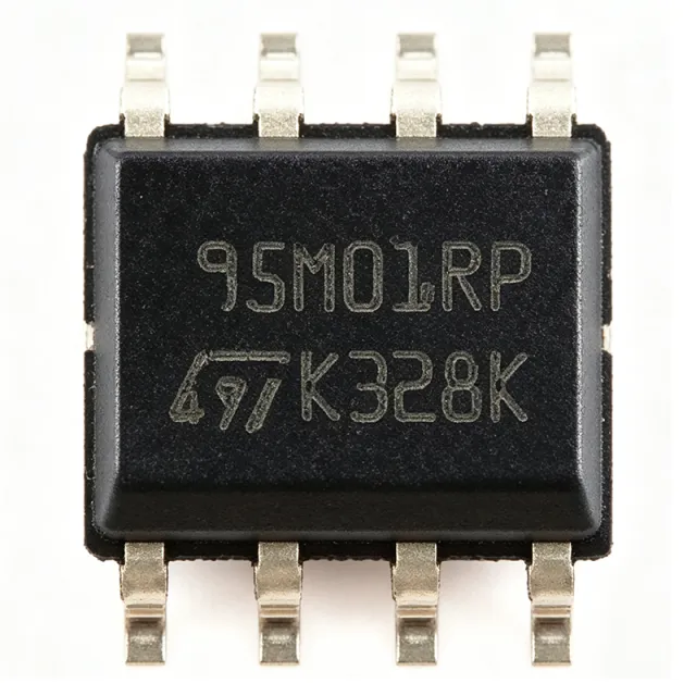
M95M01-RMN6TP - 1Mbit SPI EEPROM | STMicroelectronics
The M95M01-RMN6TP is a 1-Mbit (128 Kbyte) serial EEPROM from STMicroelectronics, organized as 131,072 x 8 bits and accessed via a high-speed SPI bus. It operates from a single 2.5V to 5.5V power supply, supports clock frequencies up to 16 MHz, and is housed in a standard 8-pin SOIC (SO-8N) package. Data verified as of 2026-08-05. An EEPROM (Electrically Erasable Programmable Read-Only Memory) is a non-volatile memory that retains data when power is removed and can be electrically erased and reprogrammed in-system. It sits within the memory hierarchy as a type of non-volatile memory, below flash memory in density but offering byte-level erase/write granularity and higher endurance for frequent small updates. In the product taxonomy, EEPROM is a subclass of memory ICs, which fall under integrated circuits, ultimately part of the broader semiconductor category. Key features include a 16 MHz SPI interface (SPI-compatible modes 0 and 0), a write time of 5 ms typical, and a write endurance of 4 million write cycles per byte. The device also offers a 200-year data retention at 55°C, a page size of 256 bytes, and a self-timed programming cycle with automatic address increment. The SO-8N package is widely used and footprint-compatible with many industry-standard EEPROMs, enabling drop-in replacement in existing designs. The M95M01 uses a standard SPI protocol with Chip Select (S), Serial Clock (C), Serial Data Input (D), and Serial Data Output (Q) pins. It includes a Write Protect (W) pin and a Hold (HOLD) pin for suspending communication without resetting the device. The memory array is organized into pages, and the device supports sequential read and write operations across page boundaries, simplifying firmware design. Typical applications include industrial automation parameter storage, smart metering data logging, medical device calibration data, and automotive electronics (non-safety-critical) where reliable non-volatile storage is required. The wide voltage range and high endurance make it suitable for frequent data updates in embedded systems. When designing with this device, ensure the SPI bus is properly terminated and that the Write Protect pin is controlled to prevent accidental writes. The HOLD pin should be pulled high if unused. For high-reliability applications, consider the device's 4 million write cycle endurance and 200-year data retention specifications. This page synthesizes distributor pricing, drop-in alternatives, and practical design notes not found in the STMicroelectronics datasheet, providing engineers with a comprehensive resource for selecting and using the M95M01-RMN6TP.
M95M02-DRMN6TP - 2Mbit SPI EEPROM | STMicroelectronics
The M95M02-DRMN6TP is a 2-Mbit (256 Kbyte) serial EEPROM from STMicroelectronics, organized as 262,144 x 8 bits and accessed via a high-speed SPI bus. It operates from a 1.8V to 5.5V supply, supports clock frequencies up to 20 MHz, and is housed in a compact SO-8N package. This device is designed for applications requiring reliable, non-volatile data storage with low power consumption and high endurance. An EEPROM (Electrically Erasable Programmable Read-Only Memory) is a type of non-volatile memory that can be electrically erased and reprogrammed. It retains data without power, making it essential for storing configuration parameters, calibration data, and small amounts of firmware in embedded systems. EEPROMs are part of the broader memory IC hierarchy: EEPROM -> serial EEPROM -> SPI EEPROM -> non-volatile memory -> semiconductor memory. The SPI interface provides a simple, high-speed serial connection using just four wires (SCK, MOSI, MISO, CS), reducing pin count and PCB area compared to parallel EEPROMs. Key features of the M95M02-DRMN6TP include a 20 MHz maximum clock frequency, byte and page write modes (up to 256 bytes per page), and a write time of 5 ms per page. It offers a write endurance of 4 million write cycles and data retention of 100 years, ensuring long-term reliability. The device also includes a hardware write-protect pin (WC) and a status register with a Write-In-Progress (WIP) bit for software polling. The SO-8N package is industry-standard, enabling drop-in compatibility with many other 2-Mbit SPI EEPROMs. Technically, the M95M02-DRMN6TP uses a floating-gate transistor architecture, which is standard for EEPROM technology. The SPI interface supports modes 0 and 3, and the device is compatible with both 3-wire and 4-wire SPI configurations. The memory array is organized into 1024 pages of 256 bytes each, allowing efficient block writes. The device also features a deep power-down mode that reduces current consumption to 1 uA, ideal for battery-powered applications. Typical applications include industrial automation for storing calibration and configuration data, smart meters for logging consumption data, and automotive electronics for storing VIN and diagnostic information. The wide voltage range and high endurance make it suitable for harsh environments. In IoT devices, it stores device credentials and sensor calibration data. When designing with this device, ensure the SPI bus is properly terminated and the CS pin is held high when the device is not selected. Use a 0.1 uF decoupling capacitor close to the VCC pin. For write operations, poll the WIP bit or wait 5 ms before initiating the next command to avoid data corruption.
MAP1001 - Gen3x4 NVMe SSD Controller | MAXIO
MAXIO Technology MAP1001 is a DRAM-based NVMe SSD controller developed around PCIe Gen3x4 connectivity and eight NAND channels. The verified source describes up to 3.5 GB/s sequential read, 3.0 GB/s sequential write, and 800,000/600,000 read/write IOPS. Its package and pin configuration are not provided in the available material. An NVMe SSD controller is a semiconductor that coordinates a host interface, NAND flash, DRAM, error correction, and data movement inside a solid-state drive. Within the storage hierarchy, it sits between the PCIe/NVMe host interface and NAND media, combining protocol handling, flash translation, wear management, and Agile ECC functions. The verified controller PDF identifies MAP1001 as part of MAXIO's DRAM-based SSD-controller family and positions it for high-performance client and edge-computing SSDs. The controller uses a Gen3x4 PCIe interface and provides eight NAND channels, distinguishing it from MAP1003, which is described as a four-channel mainstream solution. Agile ECC adds advanced correction and adaptive functionality intended to accommodate evolving NAND flash requirements. This makes the architecture relevant to SSDs requiring high throughput, interface bandwidth, parallel NAND access, and software-managed flash reliability. Typical applications include high-performance client SSDs, edge-computing storage, desktop PCs, laptops, and other PCIe-based systems that use NVMe storage. The published performance claims target sequential transfers and random IOPS, but sustained real-drive results depend on NAND type, DRAM configuration, firmware, thermal design, and workload. The eight-channel topology can improve parallelism, while the controller's PCIe generation limits the interface to the capabilities of its Gen3x4 link. A complete SSD design must account for power sequencing, high-speed PCB signal integrity, NAND and DRAM routing, thermal dissipation, firmware, ECC behavior, and validation across supported flash densities. Engineers should use the manufacturer's controller documentation for electrical limits, supported NAND devices, reference schematics, firmware requirements, and package pin assignments; those details are unavailable in the supplied sources. This page consolidates the verified MAP1001 controller identity, interface generation, NAND-channel count, architecture, and reported performance while separating documented facts from missing design data. It also records that no package, pinout, pricing, lifecycle, or verified drop-in replacement could be substantiated from the supplied evidence.
MAP1202 - PCIe 3.0 x4 NVMe SSD Controller | Maxio
The Maxio MAP1202 is a DRAMless NVMe solid-state-drive controller with a PCI Express Gen3 x4 host interface and a four-channel NAND interface supporting up to four CE devices per channel. The verified controller PDF describes the MAP1202-I as part of Maxio’s MAP1002-I, MAP1202-I, and MAP1602-I controller family. It is intended for client and edge-computing SSD designs rather than conventional discrete-logic or analog components. A DRAMless SSD controller is a semiconductor that coordinates communication between a host computer and NAND flash while supplying the data-management, error-correction, and firmware functions needed for reliable storage. In the storage hierarchy, MAP1202 is an SSD controller, which is a form of flash-storage controller and semiconductor. Its PCIe interface connects the SSD to the host, while its NAND interface connects the controller to flash devices mounted on the SSD module. Verified information identifies PCI Express Gen3 x4 host connectivity, four NAND channels, and support for as many as four devices per channel. The MAP1202-I family description also identifies Smart Cache architecture, Fusion multi-core technology, hardware/firmware co-design, and power-consumption optimization. A separate product listing identifies MAP1202 as an NVMe SSD controller, but the supplied data does not provide operating voltage, package dimensions, pin count, maximum NAND capacity, throughput figures, ECC endurance, or supported temperature grades. Typical design uses include M.2 NVMe client SSDs, edge-computing SSDs, and compact embedded storage systems requiring PCIe Gen3 x4 connectivity. The four-channel NAND interface provides a defined path for integrating multiple flash devices, but actual SSD performance depends on the selected NAND, firmware, PCB layout, thermal design, and PCIe link configuration. MAP1202 is therefore a platform component, not a complete SSD module. Engineers should verify the exact package, pinout, NAND compatibility, firmware support, and electrical limits against the applicable Maxio technical document before layout or production. Because the verified material does not establish a public, unambiguous pinout for MAP1202, this page does not infer one. It also does not treat generic controller pages or uncross-referenced parts as proof of drop-in replacement. Design decisions should use the exact controller marking and SSD reference platform.
MAP1806 - PCIe 5.0 NVMe Controller | Maxio
The Maxio MAP1806 is a PCIe Gen5 NVMe SSD controller reported with up to 14.8 GB/s performance, an 11 mm × 14.5 mm die, eight NAND channels, and four chip-enable signals in the verified search results. It is a semiconductor storage-controller component intended for high-speed solid-state drives rather than an automotive manifold-pressure sensor or unrelated catalog item with the same identifier. The available information identifies a PCIe 5.0 x4 interface and support for NAND Flash operation up to 3,600 MT/s; several electrical, package, thermal, endurance, and lifecycle values remain unavailable in the supplied data. An NVMe SSD controller is a type of semiconductor interface controller that coordinates a host PCIe link, NAND flash channels, command processing, data transfer, and storage-management functions. It sits within the hierarchy of solid-state-drive controller, storage semiconductor, PCIe interface device, and semiconductor. MAP1806 is relevant to high-capacity, high-speed NVMe SSD designs where the controller must aggregate multiple NAND devices into a reliable storage subsystem. The verified search results report eight channels with four CEs, NAND Flash speeds up to 3,600 MT/s, and a maximum SSD performance figure of 14.8 GB/s. One result associates the MAP1806A-F2C variant with a Lexar NM990 PCIe 5.0 x4 SSD, while another describes the MAP1806 as a consumer PCIe Gen5 SSD controller. These reports are useful application context, but they do not establish the complete electrical specification, pinout, package outline, or qualified replacement status. Typical uses include client PCIe 5.0 NVMe SSDs, high-speed desktop storage, workstation storage, and external storage systems that use an appropriate enclosure and thermal design. The controller should be selected only after confirming the exact package, firmware support, NAND compatibility, power requirements, signal integrity, and thermal constraints with the manufacturer. A key design consideration is that controller performance depends on the complete storage path, including NAND type, channel population, PCIe link behavior, firmware, and thermal management. Do not infer guaranteed SSD throughput from the controller headline alone. Verify the final design against the manufacturer’s current documentation and qualification information. This page separates the verified MAP1806 controller references from unrelated results that reuse the identifier for sensors, cutting tools, and hardware. It also distinguishes reported technical observations from missing datasheet data. Pricing, stock, pinout, package details, compliance, and drop-in alternatives are not established by the supplied search results and should not be treated as purchase-ready facts.
MAS0901 - SATA 6Gb/s SSD Controller | Maxio
The Maxio MAS0901 is a SATA 3.2 solid-state drive controller supporting a 6 Gb/s interface, compatibility with 2D and 3D NAND in MLC, TLC, and QLC formats, and SSD capacities up to 2 TB. The verified technical source describes Agile ECC error correction with adaptive functionality, but it does not disclose the controller package, pin count, operating voltage, process technology, or pinout. A solid-state drive controller is the central semiconductor inside an SSD. It coordinates communication between a host computer through SATA and nonvolatile NAND flash storage. Within the product hierarchy, the MAS0901 is an SSD controller, a storage semiconductor, and a data-processing IC. Its SATA link supplies command and data transfer functions, while its NAND-management and Agile ECC functions help maintain data integrity as NAND structures evolve. The principal verified capabilities are a SATA 6 Gb/s interface, support for 2D/3D MLC, TLC, and QLC NAND, and a maximum stated SSD capacity of 2 TB. The manufacturer page identifies the related MAS0901-C as a DRAM SSD controller family member designed for mainstream high-performance PC client SSDs. The independent technical PDF associates MAS0901 with DRAM-based SATA SSDs and states that Agile ECC provides advanced correction and adaptive functions. Typical MAS0901 use cases include SATA client SSDs, desktop and notebook storage upgrades, edge-computing storage, and cost-sensitive consumer systems. NAND qualification remains essential because controller firmware, flash timing, ECC behavior, and power rails must match the selected NAND package. The verified material says compatible 3D NAND is broad, but it does not provide a definitive NAND compatibility list. A critical design step is obtaining the official package drawing, pin definitions, electrical limits, reference firmware, and validation guidance before PCB release. Because those documents are not available in the supplied data, engineers should not infer a footprint or assume that a MAS0902-family device is pin-to-pin compatible. This page consolidates the verified SATA, NAND, ECC, and capacity information while explicitly identifying missing electrical, mechanical, lifecycle, and pricing data. It also separates documented capabilities from unverified drop-in alternatives, preventing an SSD-controller substitution from being treated as safe without package and firmware validation.

MB85RS256A - 256Kbit SPI FRAM Memory, 25 MHz | RAMXEED
The RAMXEED (formerly Fujitsu Semiconductor) MB85RS256A is a 256-Kbit (32,768 words × 8 bits) nonvolatile FRAM (Ferroelectric Random Access Memory) chip that communicates over an SPI bus at up to 25 MHz, housed in an 8-pin SOP (8-SOP / 150 mil) package. It uses the ferroelectric process and silicon-gate CMOS process technologies for the nonvolatile memory cells, retaining data without a back-up battery and supporting up to 10^10 read/write cycles per cell. An FRAM (Ferroelectric Random Access Memory) is a type of nonvolatile RAM that combines the fast write speed and unlimited endurance of SRAM with the data-retention behaviour of flash or EEPROM. FRAM cells store data as the polarisation state of a ferroelectric capacitor, so writes occur at bus speed (no erase/program delay) and the technology slots into the same hierarchy as SRAM -> nonvolatile memory -> memory IC -> semiconductor. This makes FRAM useful wherever systems must log data continuously without wearing out the storage medium. Key features include an operating voltage range of 2.7 V to 3.6 V (extended 2.0 V to 3.6 V for lower-speed operation), 4.5 mA active read current at 25 MHz, 2.6 uA standby current, page-mode write capability up to 32 bytes, and hardware-controlled write protection via the /WP pin. The device also supports SPI Mode 0 (CPOL=0, CPHA=0) and Mode 3 (CPHA=1), making it compatible with most microcontroller SPI peripherals. Data retention is specified at 10 years. The MB85RS256A uses a standard SPI instruction set with eight instructions (WREN, WRDI, READ, WRITE, RDSR, WRSR, FSTRD, SLEEP) and a built-in 8-byte SRAM write buffer that enables byte-aligned writes at full bus speed. Compared with EEPROM, the absence of a write cycle time means that wear-levelling firmware is unnecessary. Compared with serial flash, the device does not require an erase-before-write sequence, simplifying firmware and shortening worst-case commit latency. Typical applications include data logging for smart meters and industrial sensors, black-box event recorders, PLC/industrial automation parameter storage, medical devices requiring frequent log writes, and gaming-console cartridge save storage (the part is widely used in the Game Boy / non-volatile cart community). The wide voltage range and low standby current also suit battery-backed IoT endpoints. When designing with this part, note that the /WP pin must be tied high (inactive) for normal SPI operation, and decoupling of at least 0.1 uF should be placed within 5 mm of the VDD pin. Unlike EEPROM, FRAM has no internal charge pump and no page-write time, so write throughput equals read throughput when the buffer is kept full. This page synthesises distributor pricing, drop-in alternatives, and practical design notes not found in the manufacturer datasheet alone, helping engineers compare the MB85RS256A against newer MB85RS256B revisions and cross-brand SPI FRAM from TI, Cypress, and ROHM.
MEM-DR532MD-ER48 - 32GB DDR5-4800 ECC RDIMM 2Rx8 Server Memory | Supermicro
The Supermicro MEM-DR532MD-ER48 is a 32 GB registered ECC DDR5-4800 RDIMM server memory module rated at 4800 MT/s (PC5-38400), CL40, 1.1 V, with a 288-pin RDIMM form factor and 2Rx8 dual-rank organization. It is sold as a Supermicro OEM branded module with both Samsung and Micron DRAM variants available on the market, depending on supply. A RDIMM (Registered DIMM) is a type of server-class memory module that places a register buffer between the DRAM chips and the memory controller. This buffering reduces electrical load on the controller, enabling higher module counts per channel than unbuffered memory. Within the server memory hierarchy: DRAM chip -> DIMM -> RDIMM (buffered, ECC) -> server memory module. RDIMMs are required for most enterprise CPUs and are incompatible with consumer desktops that lack register-buffer support. Key features include 32 GB capacity in a single module, DDR5-4800 data rate (38.4 GB/s peak per module), on-module ECC for single-bit error correction, integrated PMIC for stable 1.1 V power delivery from the host, and JEDEC JESD79-5 compliance. The 2Rx8 dual-rank x8 organization provides two independent ranks of x8 DRAM devices, optimizing bandwidth on multi-channel server platforms. DDR5 RDIMMs are used in mainstream 1P and 2P server motherboards based on Intel Sapphire Rapids / Emerald Rapids and AMD EPYC 9004 (Genoa / Bergamo). Typical applications include virtualization hosts, AI inference nodes, in-memory databases, and high-density VDI clusters. When sizing platforms, ensure the host CPU memory controller supports DDR5-4800 (PC5-38400) and that the motherboard BIOS recognizes 2Rx8 32 GB RDIMMs in the validated QVL for reliable operation.

MR0A08BCYS35 - 1Mb 3.3V 35ns Parallel MRAM | Everspin TSOP-II-44
The Everspin Technologies MR0A08BCYS35 is a 1-Mbit (128K x 8) parallel Magnetoresistive Random-Access Memory (MRAM) device organized as 128K words of 8 bits each, with 35 ns asynchronous read/write access time and a single 3.3 V power supply. The part is housed in a 44-pin TSOP-II (Type II) surface-mount package and is qualified for industrial-grade temperature operation. An MRAM (Magnetoresistive Random-Access Memory) is a non-volatile memory technology that stores data in magnetic storage elements rather than electric charge. Within the broader memory taxonomy, MRAM sits between SRAM and DRAM in speed while offering non-volatility comparable to flash. MR0A08BCYS35 belongs to the parallel MRAM category, which means it uses a parallel address and data bus similar to asynchronous SRAM, allowing direct drop-in replacement for many SRAM designs where non-volatility is desired. Unlike flash, MRAM has unlimited read/write endurance and byte-level write capability without erase cycles. Key features of the MR0A08BCYS35 include a 35 ns access time equal to standard 3.3 V SRAM, byte-wide data bus, simple SRAM-like asynchronous interface (CE, OE, WE control), unlimited endurance (>10^16 cycles), 20-year data retention, and instant non-volatile write with no battery backup required. The TSOP-II-44 footprint matches standard 44-pin 1Mb / 512Kb SRAM packages used in legacy industrial designs. Internally, the MR0A08B series uses a 1-transistor, 1-magnetic-tunnel-junction (1T-1MTJ) bit cell with parallel-sense architecture that delivers SRAM-equential read latency while writing data by switching the MTJ free layer through current pulses. The result is a true random-access, non-volatile memory that requires no charge pump for writes and no wear-leveling for endurance. Typical applications for MR0A08BCYS35 include industrial control PLCs and HMIs, factory automation loggers, smart-meter data retention, gaming terminals, point-of-sale terminals, medical monitoring equipment, and any embedded system that previously used battery-backed SRAM (BB-SRAM) or NVSRAM modules. Designers migrating from CY62256, CY7C128, or similar SRAM get non-volatility without footprint changes. When designing with MR0A08BCYS35, treat it as a 35 ns SRAM: add a 0.1 uF decoupling capacitor near VCC and route CS, OE, WE with the same timing discipline as asynchronous SRAM. Note that MRAM writes are non-volatile but slightly slower than SRAM writes, and byte-write masking requires the WE-controlled protocol described in the datasheet. This page synthesizes distributor pricing from Mouser, DigiKey, LCSC, and Octopart, drop-in same-package alternatives from the Everspin MR0A08B family, and practical design notes not found in the manufacturer datasheet alone.
MR2A16ACYS35 - 4Mb 3.3V 35ns Parallel MRAM | Everspin TSOP-44
The Everspin Technologies MR2A16ACYS35 is a 4-Mbit parallel Magnetoresistive RAM (MRAM) organized as 256K words x 16 bits, housed in a 44-pin TSOP-II surface-mount package and specified for industrial-temperature operation from -40C to +85C. Key parameters are 4,194,304 bits of non-volatile storage, 35 ns read/write access time, and 3.0 V to 3.6 V (3.3 V nominal) single supply operation, in a 44-TSOP2 package. The device retains data for >20 years without power and offers SRAM-compatible asynchronous timing with unlimited read/write endurance. What is MRAM? MRAM (Magnetoresistive Random Access Memory) is a non-volatile memory technology that uses magnetic tunnel junctions (MTJs) to store each bit. MRAM sits in the hierarchy: memory IC -> non-volatile memory -> MRAM. Unlike Flash, MRAM writes without high-voltage charge pumps and unlike SRAM, MRAM retains data through power loss, combining SRAM speed with FRAM/EEPROM persistence. Key features include 35 ns read and write cycle time (effectively zero write latency versus the millisecond-class erase cycles of Flash or EEPROM), byte/word controlled write enable (/BW), chip enable (/E1, /E2), and output enable (/G) signals that emulate a standard asynchronous SRAM bus, and a low standby current typical for battery-backed designs. Data is non-volatile for >20 years and the part offers unlimited read/write endurance, eliminating the wear-out mechanisms that limit Flash. The MR2A16ACYS35 uses Everspin's field-switched Toggle MRAM cell with a parallel asynchronous interface that drops onto SRAM pinouts. Architecture is a 256Kx16 array with internal address latch, write driver, and sense amplifiers; the parallel interface supports 16-bit data bus and 18-bit address bus with /LB and /UB byte controls. Performance is SRAM-equivalent for reads (35 ns) with the bonus of instant non-volatile writes (also 35 ns). Typical applications include industrial data logging where power-loss immunity is mandatory, factory automation with battery-backed SRAM replacement, RAID controller write journals, point-of-sale terminals, smart-meter event buffers, and automotive subsystems requiring -40C to +85C temperature range. The Everspin MR2A16A datasheet documents a 20-year data-retention specification. When designing with this device, plan for a single 3.3 V supply and place a 0.1 uF decoupling capacitor close to the VDD/VSS pins. Toggle MRAM does not require the long programming delays of Flash or the wear leveling required by EEPROM, but the bus timing must respect the 35 ns tAVAV cycle time when running at full speed.
MT16LSDT3264AG-10E - 256MB PC100 SDRAM DIMM | Micron Technology
The Micron Technology MT16LSDT3264AG-10E is a 256 MB (32 Meg x 64) unbuffered, non-ECC 168-pin SDRAM Dual In-line Memory Module (DIMM) operating at 100 MHz, conforming to the JEDEC PC100 specification. The module uses a single +3.3V ±0.3V power supply and is fully synchronous to the system clock, with all signals referenced to the rising clock edge. It is organized as dual-rank and targets cost-sensitive desktop and entry-server memory upgrades that were mainstream in the PC100 era. An SDRAM DIMM (Synchronous DRAM Dual In-line Memory Module) is a printed-circuit-board assembly that places multiple SDRAM chips on a small PCB with a standardized edge-finger connector so the memory subsystem can be upgraded or replaced without soldering. SDRAM succeeded earlier asynchronous DRAM (FPM/EDO) by synchronizing all operations to the system clock, which improved burst-read/write efficiency; PC100 is the JEDEC-standard speed grade that guarantees correct operation at a 100 MHz external bus clock with a CAS latency of 2. In the broader taxonomy, SDRAM -> DRAM -> volatile memory -> semiconductor memory, sitting below non-volatile NAND/NOR flash and above SRAM in the cost/density curve. Key feature highlights for this Micron module: 100 MHz bus frequency (PC100 compliant), CAS latency 2, 168-pin unbuffered DIMM form factor, 32 Meg x 64 organization yielding 256 MB, single +3.3V ±0.3V supply, fully synchronous operation, and a dual-rank PCB assembly. The module is compatible with motherboards that expose a standard SDRAM DIMM socket (Intel 440BX, VIA Apollo Pro 133 and earlier chipsets) and supports an initial 100 µs pause followed by two AUTO REFRESH commands after power-up. The architecture is built from discrete 125/133 MHz-capable SDRAM components mounted on a multi-layer PCB with all address, control and data nets length-matched and terminated to support the 100 MHz command and data rate. Because the module is unbuffered and non-ECC, signal loading is at the minimum, which keeps the design simple but means it cannot be used in registered-memory systems such as high-end server boards of the era. Typical applications include legacy desktop PC memory upgrades, PC100-era workstation memory expansion, embedded industrial PCs, point-of-sale terminals, legacy telecom/datacom line cards, and hobbyist retro-computing projects. The combination of 256 MB density and PC100 timing keeps the module useful for reviving industrial controllers and older office PCs that still require a JEDEC-standard 168-pin SDRAM DIMM. When designing with this module, ensure the host chipset supports PC100 timing and 168-pin unbuffered DIMMs; mixing it with PC133 modules will down-clock the bus to 100 MHz. ESD handling during insertion and a proper power-supply ramp-up sequence (VDD and VDDQ must rise together) are essential for reliable initialization per the Micron datasheet. This page synthesizes distributor pricing, drop-in alternatives, and practical design notes not found in the manufacturer datasheet, giving procurement and design engineers a single decision-ready reference for legacy SDRAM DIMM selection.
MT25QL128ABA1ESE-0SIT - 128Mb SPI NOR Flash, 133MHz | Micron
The Micron MT25QL128ABA1ESE-0SIT is a 128-Mbit (16 MiB) serial NOR Flash memory with SPI/Quad-SPI bus and a maximum clock frequency of 133 MHz, housed in an 8-pin SOP2 (208-mil SOIC) surface-mount package. It operates from a single 2.7 V to 3.6 V supply, supports Quad I/O and Dual I/O transfer modes, and delivers fast read throughput suitable for code-storage and execute-in-place (XIP) applications. The device is industrial-grade (-40 °C to +85 °C), supplied in tape-and-reel packaging, and uses Micron's 65 nm NOR process technology. A Serial NOR Flash is a non-volatile memory that stores data persistently without power and exposes a low pin-count serial interface (SPI). Within the broader memory hierarchy, NOR Flash occupies the 'execute-in-place' tier - between SRAM (volatile, fastest) and NAND Flash (high-density, sequential). It offers random byte-level read access with deterministic latency, making it ideal for boot ROM, firmware storage, and data logging in embedded systems. NOR's byte-alterable erase architecture (4 KB, 32 KB, 64 KB sectors) simplifies software wear-leveling compared with NAND's block-only structure. Key features include 133 MHz single-I/O SPI clock rate, Quad I/O read throughput up to 532 Mbit/s (4 x 133 MHz), uniform 4 KB subsector erase granularity, and 100K program/erase cycle endurance per sector. The device includes a 256-byte security register with one-time-programmable (OTP) lock, hardware write-protect pin, and a deep power-down mode that drops quiescent current to a few microamps for battery-powered designs. Architecture combines a NOR cell array with a serial command state machine and an integrated 3-byte address counter supporting 24-bit addressing (16 MB). The part implements JEDEC-standard SFDP (Serial Flash Discoverable Parameters) tables for automatic device identification, plus manufacturer and device ID registers accessible via standard 9Fh/90h read commands. Status register 1/2/3 flags power-up, program/erase, and block-protect state. Typical applications include industrial IoT firmware storage, automotive infotainment boot flash, networking equipment configuration memory, and consumer device firmware. The wide operating voltage range allows direct connection to 3.3 V MCUs and SoCs without level shifters, and the small SOIC-8 footprint fits hand-held and wearable form factors. When designing with this part, place a 0.1 µF decoupling capacitor within 5 mm of the VCC pin and keep the SCK trace short (< 25 mm) to avoid ringing at 133 MHz. Use the Quad SPI mode for firmware boot to minimize XIP latency; verify CS# setup/hold timing against your host controller's reference manual. This page synthesizes distributor pricing, drop-in alternatives, and practical design notes not found in the manufacturer datasheet - useful for engineers sourcing or second-sourcing 128 Mb serial NOR Flash for embedded designs.
MT25QL128ABA1ESE-0SIT-TR - 128Mb Serial NOR Flash SPI/Quad | Micron
The Micron MT25QL128ABA1ESE-0SIT-TR is a 128 Mbit (16 MB) Serial NOR Flash memory IC supporting SPI, Dual-SPI, and Quad-SPI interfaces with a clock frequency up to 133 MHz, housed in an 8-pin SOIC (SOP2-8) package rated for 2.7 V to 3.6 V single-supply operation. This is the tape-and-reel packaging variant of the MT25QL128ABA1ESE-0SIT, sharing the same die and pinout but supplied in T&R format for high-volume SMT assembly. What is a Serial NOR Flash? A Serial NOR Flash is a non-volatile memory that stores data persistently and connects to a host processor over a low-pin-count serial interface (SPI). It belongs to the broader category of flash memory (non-volatile storage) -> NOR flash -> serial NOR flash -> SPI NOR flash. Unlike parallel NOR, serial NOR uses few pins (typically 4 to 8), making it ideal for space-constrained embedded designs. It offers fast random read access (typically tens of nanoseconds), byte-level program/erase granularity, and execute-in-place (XiP) capability, distinguishing it from NAND flash which uses sequential page access. Key features of the MT25QL128ABA1ESE-0SIT-TR include 128 Mbit density organized as 32M x 4 / 16M x 8 / 8M x 16, support for Single I/O, Dual I/O, and Quad I/O SPI modes, an industry-standard 8-pin SOIC (SOIC-8 wide-body) footprint, JEDEC JESD216-compliant SFDP register, and configurable 4 KB, 32 KB, and 64 KB sector erase sizes for flexible memory partitioning. The device uses Micron's proprietary NOR cell architecture and supports standard SPI command set including read, page program, sector/block erase, chip erase, status register read, and JEDEC ID. The Quad SPI mode enables up to 4x faster read throughput compared to standard SPI, which is critical for boot-from-flash and XIP (execute-in-place) applications in performance-sensitive embedded systems. Typical applications include firmware storage and boot ROM in networking equipment, IoT edge devices, industrial PLC controllers, automotive infotainment, set-top box firmware, and consumer electronics bootloaders. The wide 3V supply range and industrial-grade temperature support make it suitable for both consumer and industrial environments requiring reliable non-volatile code storage. When designing with this device, ensure proper PCB layout to maintain signal integrity on the SPI clock and data lines, especially at 133 MHz Quad SPI clock rates. A 0.1 µF decoupling capacitor close to the VCC pin and a 4.7 kΩ to 10 kΩ pull-up on the /CS line are recommended for reliable operation across temperature. This page synthesizes distributor pricing, drop-in same-package alternatives, and practical design notes not found in the manufacturer datasheet alone, including same-footprint Micron variants (MT25QL128ABA1ESE-0SIT base part) and validated cross-brand SPI NOR Flash equivalents.

MT25QL128ABA8ESF-0SIT - 128Mbit SPI/Quad-SPI NOR Flash | Micron
The Micron MT25QL128ABA8ESF-0SIT is a 128 Mbit (16 MB) serial NOR flash memory with SPI/Quad-SPI interface, supporting clock rates up to 133 MHz in a 16-pin SOIC (SO-16) package. Operating from 2.7V to 3.6V, it uses single-bit, dual, and quad I/O modes, with a 6 ns access time enabling fast random-read throughput for boot, code-shadowing, and data-logging tasks. A NOR flash memory is a non-volatile storage technology where each cell behaves like a MOSFET with a floating gate, giving byte-level random read access and faster read latency than NAND, at the cost of lower density and slower write/erase. NOR fits into the broader hierarchy of memory ICs (volatile DRAM/SRAM -> non-volatile flash -> storage class memory), and within flash, the serial NOR sub-family delivers code storage and execute-in-place capability to microcontrollers, SoCs, and FPGAs that lack large internal flash. Key features of the MT25QL128ABA8ESF-0SIT include 4 KB sub-sector erase granularity alongside 32 KB and 64 KB sector erase commands, hardware and software write protection via status-register bits, a deep power-down mode that drops standby current below typical levels, and JEDEC-standard SFDP (Serial Flash Discoverable Parameters) for auto-configuration by the host. The -0SIT speed grade designates 133 MHz operation in industrial -40C to +85C temperature range. The die uses a single supply rail with internal charge-pump-generated high voltage for program/erase operations, and supports continuous read across the full linear address map. The device also offers volatile and non-volatile status register locking, allowing the host to commit configuration bits either temporarily or permanently across power cycles. Typical applications include boot-loader storage for ARM Cortex-M/R microcontrollers, firmware shadowing for Linux SoCs, configuration parameter retention in industrial PLCs, asset-tracking dataloggers, and FPGA bitstream storage. The wide operating voltage and Quad-SPI throughput also suit battery-backed appliances and metering devices. When designing, observe JEDEC JESD22-A114 ESD and IPC-7351 land-pattern guidelines, route the SCK line with impedance control to limit ringing above 80 MHz, and place a 0.1 uF decoupling capacitor within 3 mm of the VCC pin. Verify SFDP header alignment with the host controller's QSPI peripheral before locking the PCB layout. This page consolidates verified Micron datasheet data, distributor pricing, same-package drop-in alternatives, and design considerations that go beyond the datasheet's typical-application section, helping engineers select and source this part quickly.
MT25QL128ABA8ESF-0SIT-TR - 128Mb Serial NOR Flash, SPI/Quad, 16-SO | Micron
The Micron MT25QL128ABA8ESF-0SIT-TR is a 128 Mbit (16 MB) serial NOR Flash memory organized as 32M x 4, fabricated in CMOS SLC technology and housed in a 16-pin SOIC (SO-16, 300 mil) package supplied on Tape and Reel. It supports a single 3V supply (2.7V to 3.6V) and provides a clock frequency of 133 MHz maximum in Single Transfer Rate (STR) mode and 90 MHz maximum in Double Transfer Rate (DTR) mode across the SPI bus and its extended variants. The interface supports Single I/O, Dual I/O, Quad I/O, QPI, and the Micron Extended SPI protocol for a maximum throughput of 90 MB/s in DTR Quad mode. Page-program granularity is 256 bytes, sector erase is 4 KB and 32 KB, and full chip erase is supported via dedicated commands. The device is specified over the industrial -40C to +85C temperature range. A NOR Flash is a non-volatile memory that supports random-byte read access and execute-in-place (XIP) operation, sitting in the memory hierarchy between ROM and serial NAND Flash. Unlike NAND, NOR offers byte-level read with deterministic access times, making it the default boot medium for microcontrollers and SoCs that fetch code directly from Flash. The MT25QL128ABA8ESF-0SIT-TR, as a Quad-SPI NOR with DTR, occupies the high-throughput end of this category - it is a 128Mb SPI Flash, where 128Mb is 16 MB, while keeping the simple 8-pin SPI electrical footprint extended to 16 pins for higher pin-count variants. Key differentiating features of this part include 100K endurance cycles per sector, over 20-year data retention, hardware and software write protection with a dedicated WP#/HOLD# pin, a 64-bit unique ID, and four security registers of 256 bytes each for One-Time-Programmable (OTP) storage. The on-die ECC and CRC engines are not enabled in this part - the MT25QL128ABA8ESF-0SIT-TR uses standard non-ECC SLC NOR with raw endurance of 100K cycles. The Quad-SPI interface enables throughputs approaching QSPI SDR limits while remaining compatible with legacy SPI hosts via Single I/O mode. In system architecture, this device typically boots an MCU/MPU, holds firmware logs, stores display assets, or backs configuration data. Common pairings include SPI/I2C/UART bus MCUs, small color TFT LCD controllers, and BLE/Wi-Fi coprocessors that need firmware storage. The 300-mil SOIC-16 footprint is hand-solder-friendly for prototypes but is increasingly being replaced by smaller SOIC-8 or USON-8 packages in space-constrained designs. Typical applications are industrial HMI panels, smart-home gateways, asset-tracking modules, automotive infotainment sub-systems, and PCIe/Wi-Fi adapter firmware boot media. The 16-pin SO-16 footprint gives a generous 0.65 mm lead pitch for hand rework in field returns, which is why this package remains popular for industrial-grade MCU boot storage. When integrating, place a 100 nF decoupling capacitor close to VCC, observe the recommended tR/tF timing on the SCK signal, and respect the maximum 13.5 mA active read current on the VCC rail. According to Micron datasheet mt25q_qlhs_L_128_ABA (Rev. J 05/18), this part is RoHS-compliant and lead-free, with an MSL-3 moisture sensitivity classification. This page consolidates distributor pricing, drop-in alternatives, and practical design notes not found in the manufacturer datasheet alone - a synthesis intended to support engineers during part selection and second-source qualification.
MT25QU256ABA1EW7-0SIT - 256Mb 1.8V Quad SPI NOR Flash | Micron
The Micron MT25QU256ABA1EW7-0SIT is a 256 Mbit (32 MB) Serial NOR Flash memory organized as 64M x 4 / 32M x 8 / 16M x 16, supporting standard SPI, Dual SPI, Quad SPI, and Octal (DTR) I/O protocols in an 8-pin W-PDFN (6x5 mm, MLP8) package. It operates from a 1.7 V to 2.0 V supply with a 133 MHz clock in Quad I/O mode and provides 6 ns initial access latency, making it well-suited for code-storage and execute-in-place (XiP) designs. A NOR Flash is a non-volatile memory that stores bits in a parallel NOR array, giving true random-read access (byte/word addressable, like SRAM) but slower writes than NAND. It sits at the boot/ROM layer of the storage hierarchy above raw NAND (NSID) and managed NAND (eMMC/UFS), and is preferred for firmware, BIOS, FPGA bitstreams, and IoT boot images where deterministic read latency and high reliability matter more than density-per-dollar. Key features include 256 Mb density, 1.8 V single supply (1.7 V min), 133 MHz Quad SPI throughput, 6 ns access time, hardware/software write protection, a 256-byte security register with OTP bits, and 100K program/erase endurance per sector with 20-year data retention. The 8-WPDFN package exposes an EP thermal pad that doubles as the VSS reference, enabling compact board layouts under 50 mm². Architecturally, the device uses a 65 nm NOR process with a uniform 4 KB sector granularity and three flexible erase sizes (4 KB, 32 KB, 64 KB), supporting the JEDEC JESD216 SFDP register for auto-discovery. Micron's MT25Q family extends the legacy M25P/JS28 command set with extended 4-byte addressing for the >128 Mb densities. Typical applications include industrial IoT gateways requiring fast secure boot, networking switches storing firmware images, automotive infotainment boot ROMs, FPGA configuration memory for Xilinx 7-Series and Intel Cyclone families, and consumer wearables running RTOS images from external flash. The -40 °C to +85 °C industrial temperature range (-SIT suffix) makes it appropriate for harsh environments without AEC-Q100 qualification. When designing, place a 0.1 µF decoupling capacitor within 2 mm of the VCC pin and observe PCB trace length matching on CLK/IO0 to keep rise times below 2 ns. The HOLD# and WP# pins require pull-ups if unused, per the Micron reference schematic; otherwise Quad SPI boot on certain MCUs will not enumerate the device correctly. This page synthesizes distributor pricing as of 2026-10-05, drop-in alternatives, and application notes not collated on a single manufacturer page, with explicit [DATA_NEEDED] markers where the verified web data did not disclose a parameter.