Микросхемы памяти
Подкатегории
Товары (875)

M29F800FT55N3F2 - 8Mbit 5V NOR Flash 55ns | Micron
The Micron M29F800FT55N3F2 is an 8 Mbit (1 Mbit x8 / 512 Kbit x16) parallel NOR Flash memory operating from a single 5V supply, with a 55 ns access time, housed in a 48-pin TSOP package supplied in tape and reel (T/R). Parallel NOR Flash is a non-volatile memory technology that connects directly to a microprocessor's address and data buses, allowing code to be executed in place (XIP) without first copying to RAM. Within the memory hierarchy, NOR Flash sits alongside SRAM and DRAM in embedded systems as the primary boot and code-storage medium, complemented by NAND Flash and serial SPI Flash for bulk data storage. Its random-access architecture, with access times measured in nanoseconds, is what distinguishes NOR from block-oriented NAND devices. Key features of the M29F800FT55N3F2 include dual organization (1M x8-bit or 512K x16-bit, selectable via the BYTE pin), a fast 55 ns access time suitable for zero-wait-state microprocessor interfacing, single 5.0V supply for both read and write/erase operations, and a top boot block architecture (T suffix) that places the protected boot code block at the top of the memory map. The device is programmed in-system using the standard 5.0V VCC supply; no separate 12V VPP is required for program or erase operations. The memory array is organized into uniformly sized blocks with hardware sector-protection capability, block erase, and fast word/byte programming. The 48-pin TSOP surface-mount package keeps the footprint compact for embedded CPU boards, and the tape-and-reel suffix (T/R in the N3F2 ordering code) supports automated pick-and-place assembly in volume production. Typical applications include boot code storage for industrial controllers, telecom line cards, networking equipment, set-top boxes, and legacy 5V embedded systems where in-place code execution and long-term data retention are required. The 5V-only operation makes it a direct fit for older microprocessor families that run on 5V rails. When designing with this device, verify whether your boot code must reside in the top or bottom of the address map: the FT (top boot) and FB (bottom boot) variants share the same package and pinout but differ in block ordering. Always confirm block organization against your linker map before substituting. This page synthesizes distributor pricing, same-family drop-in alternatives, and practical design notes not found in the manufacturer datasheet, with pricing referenced as of 2026-09-05.
M29W064FB70N3F - 64Mb NOR Flash 70ns AEC-Q100 | Micron Technology
The Micron Technology M29W064FB70N3F is a 64 Mbit (8M x8 / 4M x16) parallel NOR flash memory with 70 ns access time, 2.7V to 3.6V supply range, and AEC-Q100 automotive qualification, housed in a 48-pin TSOP package supplied on tape and reel. Parallel NOR flash is a non-volatile memory technology that connects directly to a processor's address and data buses, allowing random access to any byte or word for in-place code execution (XIP). In the memory hierarchy, NOR flash sits alongside SRAM and SDRAM as a code-storage medium: it does not offer the density of NAND flash, but its fast random read access and high reliability make it the default boot and firmware memory for embedded systems. Key features of the M29W064FB70N3F include the x8/x16 bus-width selectable architecture via the BYTE# pin, a 70 ns access time suitable for zero-wait-state operation at moderate bus frequencies, and block-protected boot-block sector organization (FB = boot block bottom). The device supports single 3V/3.3V supply operation, fast program and erase operations with status polling, and an operating temperature range of -40C to +125C for automotive and industrial environments. Technically, the device uses a page-mode architecture with the array organized as 64 Mbit of floating-gate cells; erase granularity is asymmetric boot blocks plus main blocks, and programming uses the standard command-set interface familiar to users of the M29W family. The RY/BY# output provides hardware status indication without bus polling. Typical applications include automotive ECU boot firmware, telematics and infotainment modules, industrial PLCs, networking equipment code storage, and set-top box firmware. Design consideration: because the part is flagged obsolete in recent distributor parametric data, plan last-time-buy quantities or validate a drop-in M29W064F variant early in the design cycle. This page synthesizes verified distributor pricing, drop-in alternatives, pinout, and practical design notes not found in a single manufacturer datasheet.

M29W128GH70N3F - 128Mb 3V NOR Flash 70ns TSOP-56 | Micron
The Micron M29W128GH70N3F is a 128 Mbit (16 MB) 3V parallel NOR flash memory with a 70 ns access time, -40C to +125C operating temperature range, and a 56-lead TSOP package. A parallel NOR flash memory is a nonvolatile semiconductor storage device that allows random access to any address directly over a parallel address and data bus, distinguishing it from NAND flash and serial (SPI) NOR flash. Within the memory hierarchy, NOR flash sits alongside DRAM, SRAM, and EEPROM as a core memory IC category, and its execute-in-place (XIP) capability makes it the traditional choice for storing boot code and firmware in embedded systems. Key features of the M29W128GH include the 128 Mbit density organized for x8/x16 operation, a fast 70 ns access time that supports zero-wait-state code execution at moderate bus speeds, and an extended industrial temperature range of -40C to +125C suitable for harsh-enough environments in industrial and networking designs. The device operates from a single 3V supply (VCC), simplifying power-tree design compared with dual-rail legacy flash generations. Technically, the M29W family succeeds the STMicroelectronics M29W heritage that became part of Micron via Numonyx. The architecture divides the array into independently erasable blocks, and the command set is compatible with common CFI (Common Flash Interface) JEDEC-style programming flows, enabling reuse of established low-level flash drivers. The H suffix denotes the high-density family member with its specific block organization, while the GL variant offers a mirrored block arrangement. Typical applications include boot firmware storage in industrial controllers, set-top boxes, networking line cards, telecom equipment, and legacy embedded processors with a parallel memory bus that require reliable code storage and field firmware updates. A key design consideration is bus loading: with a parallel interface, the 70 ns access time is only achieved with proper address-line termination and controlled trace lengths, and designers should verify timing against the host controller at the full industrial temperature range. This page synthesizes distributor sourcing data, same-family drop-in options, and practical design notes not consolidated in the manufacturer datasheet, with pricing verified as of 2026-09-05.

M29W128GL70ZA3E - 128Mb NOR Flash 70ns 64-TBGA | Micron
The Micron M29W128GL70ZA3E is a 128 Mbit parallel NOR Flash memory organized as 8M x16 or 16M x8, with a 70 ns access time, operating from a 3V/3.3V supply and housed in a 64-ball TBGA (10x13 mm) package. Parallel NOR Flash is a nonvolatile memory technology in which every cell connects to a bit line, enabling true random access with short read latencies. Within the memory hierarchy, NOR Flash sits as code storage between mask ROM and NAND Flash: unlike NAND, it supports execute-in-place (XIP), allowing a processor to boot directly from the array without copying code to RAM first. It remains the standard boot memory for microcontrollers, DSPs, and FPGAs. Key features of the M29W128GL include the dual x8/x16 bus configuration selected by the BYTE pin, a fast 70 ns access time that supports zero-wait-state reads on many embedded processors, and a 3.0V to 3.6V supply range. The device provides block-protected operation, program/erase via standard command sets, and an industrial operating temperature range of -40C to +125C per Micron product data. Architecturally, the M29W128GL family uses a banked array with boot-block segmentation (the GL suffix denotes the bottom-boot variant; GH denotes top boot), enabling firmware storage with parameter blocks at the boot region. Read, program, and erase operations are controlled through standard bus command sequences with status polling. Typical applications include boot firmware storage for industrial PLCs, telecom line cards, set-top boxes, networking equipment, and automotive-adjacent control modules requiring wide temperature operation. Design-wise, verify VCC decoupling at each supply ball and confirm the BYTE pin is strapped correctly for the chosen bus width, since a floating BYTE pin causes bus contention during boot reads. This page synthesizes distributor pricing, drop-in alternatives, and practical design notes not found in the manufacturer datasheet.

M29W128GL70ZS3F - 128Mb Parallel NOR Flash 70ns | Micron
The Micron M29W128GL70ZS3F is a 128 Mbit parallel NOR Flash memory with a 70 ns access time, organized as 16M x 8 or 8M x 16, powered from a single 3V/3.3V supply and housed in a 64-ball FBGA (11x13 mm) package. Parallel NOR Flash is a nonvolatile memory technology that allows random byte-level access over a wide parallel address/data bus, making it suitable for code storage where the processor executes directly from flash (XIP, execute-in-place). In the memory hierarchy, NOR Flash sits alongside SPI NOR and NAND Flash as a nonvolatile storage class; parallel NOR offers the fastest random read latency and the simplest CPU interface, at the cost of higher pin count compared to serial NOR. Key features of this device include the 128 Mbit density, a fast 70 ns random access time for zero-wait-state code execution on many embedded processors, dual x8/x16 bus organization for bus-width flexibility, and an extended operating temperature range of -40C to +125C. The part is AEC-Q100 qualified and marketed by Micron as automotive grade, supporting design reuse in vehicular applications. The uniform 64/64 block architecture referenced by distributors indicates two symmetric partitions for flexible code and data placement. Technically, the M29W128GL family operates from a single 3V to 3.6V VCC supply, uses block-erase program/erase operations with internal state machine control, and provides status signaling for software polling. The 64-ball FBGA (11x13) surface-mount package minimizes board area while supporting the wide parallel bus required for fast random access. Typical applications include automotive ECU boot code storage, industrial PLC firmware, networking equipment boot loaders, and set-top-box or telecom designs that execute code directly from NOR Flash. A key design consideration is supply-rail integrity: verify that the 3.3V rail tolerance and program voltage requirements in the official datasheet match your system before finalizing the power tree. This page synthesizes distributor pricing, drop-in alternative analysis, application guidance, and FAQ content not found in the manufacturer datasheet alone, based on data verified as of 2026-09-05.
M29W160EB70N3E - 16Mbit NOR Flash 70ns 48-TSOP | Micron
The Micron Technology M29W160EB70N3E is a 16 Mbit (2M x8 / 1M x16) 3V parallel NOR Flash memory with a 70 ns access time, supplied in a 48-lead TSOP (48-TFSOP, 0.724 in / 18.40 mm width) package. It operates from a single VCC supply of 2.7V to 3.6V for program, erase, and read operations. Parallel NOR Flash is a nonvolatile memory organized so the host processor can execute code directly from it (XIP, execute-in-place) over a parallel address/data bus. In the memory hierarchy it sits as a boot/code storage device between mask ROM and serial NOR Flash, offering random access over a wide parallel bus rather than a serial SPI interface. NOR Flash remains the standard choice for MCU and processor boot firmware because of its fast random-access latency and byte-level readability. Key features of the M29W160EB family include a 70 ns access time suitable for zero-wait-state code execution, a block-organized architecture with boot-block arrangement, and a 10 microsecond typical programming time per byte/word. The device supports both byte (x8) and word (x16) organization, letting the designer trade data-bus width against address range without changing the PCB. Technically, the device uses a floating-gate NOR cell array with an on-chip state machine that handles program and erase algorithms, status reporting, and data protection. Command-set operation follows the industry-standard M29W command interface, allowing software drivers to poll status rather than time program/erase cycles. Supply range of 2.7V-3.6V matches common 3.3V logic rails directly. Typical applications include boot-firmware storage in industrial controllers, set-top boxes, networking equipment, telecom line cards, and automotive/white-goods control boards where a legacy parallel NOR footprint must be maintained. Design consideration: on 70 ns access-time parts, ensure address setup and output-enable timing in the host memory controller match the -70 speed grade, and keep VCC within 2.7V-3.6V during erase operations since erase voltage margin is tighter than read margin. This page synthesizes distributor pricing, verified drop-in alternatives, and practical design notes not found in the manufacturer datasheet.
M29W160EB70N3F - 16Mbit NOR Flash, 70ns, 48-TSOP | Micron
The Micron M29W160EB70N3F is a 16 Mbit (2M x8 / 1M x16) 3V parallel NOR Flash memory with a 70 ns access time, bottom boot block architecture, and a 48-pin TSOP (0.724 in / 18.40 mm width) package supplied in tape and reel packing. It operates from a single VCC supply of up to 3.6V for program, erase, and read operations, and carries AEC-Q100 automotive qualification for harsh-environment deployments. Parallel NOR Flash is a non-volatile memory technology in which each cell connects to a bit line, enabling true random-access reads at the byte or word level. In the memory hierarchy, NOR Flash sits as code-storage memory -> non-volatile memory -> solid-state storage; unlike NAND Flash, its execute-in-place (XIP) capability lets microcontrollers boot directly from the array without first copying code to RAM, which is why parallel NOR remains the default boot memory in automotive ECUs, industrial controllers, and telecom line cards. Key features of the M29W160EB70N3F include the 70 ns address-to-output access time (a 90 ns speed grade also exists in the family), a 10 microsecond typical programming time per word or byte, block-erase architecture with bottom boot blocks for reset/interrupt vector storage, and byte-wide (x8) or word-wide (x16) bus configuration selectable via the BYTE# pin. The common flash interface (CFI) lets programmers auto-detect device geometry and timing. The device is part of the Micron M29W160E family, second-generation 3V NOR Flash built on a mature floating-gate CMOS process. Program and erase commands follow a standard command-set interface compatible with common flash programmers, and the RESET# input restores the device to read mode for fast boot recovery. Automotive-grade screening supports extended temperature operation. Typical applications include automotive powertrain and body-control ECU boot code storage, industrial PLC firmware memory, networking equipment configuration storage, and set-top-box software retention. The parallel interface and 70 ns speed make it a direct fit for legacy bus designs tied to classic microcontrollers. Design consideration: at x16 operation all 16 data lines must be routed with matched length where the CPU clock exceeds 50 MHz; decouple VCC with 100 nF ceramic capacitors at each supply pin. This page adds value beyond the datasheet by synthesizing distributor pricing, drop-in alternatives with package-match verification, and practical design notes in one place.

M29W160EB80ZA3SE - 16Mb NOR Flash 80ns TFBGA-48 | Micron
The Micron Technology M29W160EB80ZA3SE is a 16 Mbit (2M x8 / 1M x16) 3V parallel NOR Flash memory with an 80 ns access time, supplied in a 48-ball TFBGA (6x8 mm footprint, 0.8 mm ball pitch) package. It operates from a 2.7V to 3.6V supply for program, erase, and read operations. Parallel NOR Flash is a nonvolatile memory technology in which every byte is directly addressable over a parallel address and data bus, allowing a processor to execute code in place (XIP) without first copying it to RAM. In the memory hierarchy it sits alongside NAND Flash and serial NOR: NAND offers higher density at lower cost per bit, while parallel NOR offers faster random access, simpler interfacing, and superior reliability, making it a staple of the embedded memory and code storage family. Key features of the M29W160EB include its byte-wide (x8) and word-wide (x16) selectable parallel interface, 80 ns random-access time for zero-wait-state code execution from many microcontrollers, and block-protected boot-block architecture that safeguards resident code from accidental erase. Program and erase operations are commanded through standard JEDEC-style command sets, with status polling and suspend/resume capability that lets the CPU service interrupts during slow erase cycles. Technically, the device uses a single 3V supply rail (2.7V to 3.6V) for all operations, eliminating dual-rail programming supplies required by older 12V-programmed Flash generations. Automotive-grade variants of the M29W160EB family carry AEC-Q100 qualification and support operation from -40C up to +125C, addressing under-hood and mission-critical environments. The TFBGA-48 ball-grid package provides low profile, small footprint, and good thermal and mechanical performance for space-constrained boards. Typical applications include automotive ECU boot code storage, industrial PLC firmware, telecom and networking equipment configuration memory, and set-top box or consumer appliance BIOS storage, where in-place code execution and long-term data retention matter more than raw write bandwidth. A key design consideration: layout for the 0.8 mm-pitch TFBGA requires careful escape routing and signal integrity practice on the parallel address bus; also budget erase time (typically hundreds of milliseconds per block) in your firmware scheduler and use suspend/resume to keep the CPU responsive. This page adds value beyond the datasheet by synthesizing distributor pricing (LCSC from $1.3460), drop-in same-package alternatives, comparison tables, and practical design notes in one engineer-ready reference.
M29W160ET70N3E - 16Mb 3V Parallel NOR Flash 70ns TSOP48 | Micron
The Micron M29W160ET70N3E is a 16 Mbit (2 Mbit x8 / 1 Mbit x16) 3V parallel NOR flash memory with a 70 ns access time, housed in a 48-pin TSOP package and qualified to AEC-Q100 for automotive applications. Parallel NOR flash is a nonvolatile memory technology in which the memory array is addressed directly over a parallel address and data bus, allowing a processor to execute code in place (XIP) without first copying it to RAM. Within the memory hierarchy, NOR flash sits alongside DRAM and SRAM as a main-memory-class device and serves as the boot and code-storage medium in automotive ECUs, industrial controllers, and set-top boxes. Its byte-granular random access and long data retention distinguish it from NAND flash, which offers higher density but only page-based access. Key features of the M29W160ET70N3E include the 70 ns random-access speed class for zero-wait-state code execution, a dual 8-bit/16-bit bus configuration selected by the BYTE# pin, and a top boot block architecture (the T in the part number) that places the protected boot code at the top of the memory map. The part number suffix E denotes the RoHS-compliant package with standard packing in tray format. Micron's M29W160E family also offers a bottom boot variant (M29W160EB) for designs whose boot code resides at address 0x000000. Architecturally, the device is organized into uniform blocks with boot blocks, and supports block erase and word/byte program operations with hardware sector protection. The supply operates from a nominal 3V/3.3V rail, and the AEC-Q100 qualification targets the extended temperature ranges typical of under-hood and body-electronics environments. Program and erase automation is handled on-chip, offloading the host microcontroller. Typical applications include automotive ECU boot code storage, industrial PLC firmware, telecom line-card configuration memory, and legacy x16 code-storage upgrades where TSOP48 footprints must be maintained. When designing in this device, verify the boot block location (top versus bottom) matches the processor's reset vector, and confirm the 70 ns access time meets the bus timing at the target VCC corner. This page synthesizes distributor pricing, drop-in alternatives, and practical design notes not found in the manufacturer datasheet.
M29W160ET70N3F - 16Mb 70ns AEC-Q100 NOR Flash | Micron
The Micron M29W160ET70N3F is a 16 Mbit (2 M x 8 / 1 M x 16) 3V/3.3V parallel NOR Flash memory with 70 ns access time, AEC-Q100 automotive qualification, and a 48-pin TSOP package supplied in tape-and-reel packing. Decoding the Micron part-number scheme, M29 denotes parallel Flash, 16 the 16 Mb array, T the top-boot block architecture, 70 the 70 ns speed grade, N3 the 48-pin TSOP, and F the RoHS-compliant tape-and-reel packing option. Parallel NOR Flash is a non-volatile memory technology in which the memory cells are connected in parallel, allowing random access to any address in a single access cycle. Within the memory hierarchy, NOR Flash sits alongside DRAM and NAND Flash as a semiconductor memory device; unlike NAND, NOR offers byte-level random access and high reliability, which is why it has long been the dominant choice for code storage (XIP, execute-in-place) in embedded systems. Key features of the M29W160ET70N3F include the 70 ns access time for fast code execution, the flexible x8/x16 bus configuration that lets designers choose between an 8-bit or 16-bit data path, and the top-boot block organization that protects boot code in the highest address blocks. Supply voltage is specified in the 3V/3.3V range per the part description. The device is built on CMOS technology and is AEC-Q100 automotive qualified, meaning it has passed the automotive industry stress-test standard for reliability, supporting temperature-grade requirements typical of in-vehicle applications. Block protection and program/erase operations follow the standard M29W160E family command set. Typical applications include automotive ECU boot-code storage, industrial control firmware, telecom and networking line-card code memory, and embedded systems requiring execute-in-place code storage from a parallel bus. Design consideration: verify the top-boot versus bottom-boot variant against your boot-vector address mapping, since selecting the wrong boot orientation inverts the location of the protected boot blocks. This page synthesizes distributor pricing context, drop-in alternatives, and practical design notes not found in the manufacturer datasheet.
M29W160FB70N3E - 16Mb 3V Parallel NOR Flash 70ns | Micron
The Micron Technology M29W160FB70N3E is a 16 Mbit (2M x8 / 1M x16) 3V parallel NOR Flash memory with a 70 ns access time, housed in a 48-pin TSOP (0.724 in / 18.40 mm width) package. Parallel NOR Flash is a nonvolatile memory technology that allows random access to any byte via a parallel address bus, making it suitable for code storage (XIP - execute-in-place) in embedded systems. Within the memory hierarchy, it belongs to the Flash memory family, alongside NAND Flash and serial NOR (SPI) devices, and is commonly used as the boot memory of a microprocessor-based system because of its fast random read capability and high reliability. Key features of the M29W160FB include a single 3.0 V to 3.6 V supply (VCC) for program, erase, and read operations, 70 ns access time, boot block architecture, and dual x8/x16 bus configurations selected by the BYTE# pin. Block-protected operation and command-set-programming via standard commands simplify firmware drivers. The device uses Micron's advanced NOR Flash cell technology with internal program and erase state machines. Program and erase operations are monitored via data polling and toggle-bit status, allowing simple software integration. Typical block program times and erase times are specified in the manufacturer datasheet. Typical applications include set-top boxes, networking and telecom equipment boot code, industrial control firmware storage, automotive infotainment modules (non-safety), and legacy embedded processor systems requiring parallel NOR. Design consideration: because this is a mature parallel NOR product family, verify lifecycle status and secure a last-time-buy strategy or pin-compatible second source early in new designs. This page synthesizes distributor pricing, drop-in alternatives within the M29W160 family, and practical design notes not found in the manufacturer datasheet.

M29W320DB80ZA3E - 32Mb Parallel NOR Flash 80ns | Micron
The Micron Technology M29W320DB80ZA3E is a 32 Mbit parallel NOR Flash memory organized as 4M x 8 or 2M x 16, with an 80 ns access time, housed in a 63-ball TFBGA (7x11 mm) package operating from a 2.7V to 3.6V supply. Parallel NOR Flash is a non-volatile memory technology that allows random access to any address, making it ideal for storing boot code and firmware that a processor executes directly in place (XIP). Unlike NAND Flash, NOR offers fast random read access and byte-level addressing, sitting within the memory hierarchy as a code-storage device alongside SRAM and DRAM in embedded systems. Key features of the M29W320DB include non-uniform block architecture with boot block organization (the DB suffix denotes bottom boot block), 64 KByte main blocks plus parameter blocks, and a VCC supply of 2.7V to 3.6V for program, erase, and read operations. An optional VPP pin supports a 12V supply for fast program operations. The 80 ns access time supports zero-wait-state execution from slower buses. The device uses Micron (formerly STMicroelectronics/Numonyx) NOR Flash core technology with command-set compatibility to the industry-standard M29W family, including single-word/byte programming, block erase, and status polling via data or toggle bits. Erase suspend/resume allows the host to interrupt block erasure to service read requests, keeping real-time code execution alive during maintenance operations. Typical applications include set-top boxes, automotive instrument clusters and body controllers, industrial PLCs, networking equipment boot firmware, and medical devices where code shadowing or execute-in-place from a reliable parallel NOR device is required. When designing, respect the 80 ns access-time derating across the full automotive temperature range and provide proper VCC decoupling during program and erase, which draw higher transient currents. This page synthesizes distributor pricing, drop-in alternatives, and practical design notes not found in the manufacturer datasheet.
M29W320DT70N3E - 32Mbit NOR Flash 70ns 48-TSOP | Micron
The Micron M29W320DT70N3E is a 32 Mbit parallel NOR Flash memory organized as 4M x8 or 2M x16 bits, with a 70 ns access time, operating from a single 2.7 V to 3.6 V supply in a 48-pin TSOP I package. A parallel NOR Flash memory is a non-volatile semiconductor memory in which cells are individually addressable over a parallel address/data bus, allowing random access and direct code execution (XIP) by a microprocessor. Within the memory hierarchy, it sits alongside and complements DRAM (volatile working memory) and NAND Flash (bulk storage): NOR provides fast read latency and byte-level random access, which is why boot code, firmware, and parameter storage have historically been placed in NOR devices. Key features of the M29W320DT include its asymmetrically arranged memory blocks, where a boot region of 64 Kbytes is subdivided into a 16 Kbyte boot block, two 8 Kbyte parameter blocks, and one 32 Kbyte small main block, with remaining capacity in large main blocks. The 70 ns access time supports zero-wait-state code execution from many microprocessors. The device supports read, erase, and program operations from the single low-voltage supply, and programming is performed via standard command-set interfaces familiar to legacy M29W-series designers. Technically, the part is a member of the Micron (ex-STMicroelectronics) M29W320D family; the DT suffix denotes top boot-block architecture, versus DB for bottom boot. The N3E ordering code indicates the 70 ns speed grade, 3 V operating range, TSOP I 48-lead package, and lead-free/ECO packaging revision. Peak reflow time is rated at 30 seconds with Moisture Sensitivity Level 3 (168 hours floor life per AIChipLink product data). Typical applications include microprocessor boot firmware storage in industrial controls, set-top boxes, networking equipment line cards, and telecom modules where code shadowing or XIP is required. The parameter blocks suit configuration and calibration data storage alongside the main firmware region. Design consideration: verify supply decoupling and bus turnaround timing, because at 70 ns the read cycle margin is tight with slow external latches; also confirm block orientation (top boot) matches the CPU reset vector mapping. This page synthesizes distributor pricing, drop-in alternatives, cross-reference findings, and practical design notes not found in the manufacturer datasheet.
M29W640GB70N3F - 64Mb 70ns Parallel NOR Flash | Micron
The Micron Technology M29W640GB70N3F is a 64Mb (8 MB) 3V parallel NOR flash memory with x8/x16 data-bus width, 70 ns access time, and an operating voltage range of 2.7V to 3.6V, housed in a 48-lead TSOP I package and qualified to AEC-Q100 for automotive environments with a -40C to +125C operating temperature range. Parallel NOR flash is a nonvolatile memory technology in which every address is directly accessible over a parallel address/data bus, giving deterministic read latency. In the memory hierarchy it sits alongside NAND flash and serial (SPI) flash as a code-storage device; NOR's execute-in-place (XIP) capability and superior random-read speed make it the traditional choice for boot code, firmware, and parameter storage in microcontroller-based systems, whereas NAND targets high-density data storage. Key features of the M29W640GB include the 70 ns access time for fast code fetch, a flexible x8/x16 organization that lets one footprint serve 8-bit or 16-bit buses, 2.7V-3.6V single-supply operation for 3V embedded systems, and automotive AEC-Q100 qualification over the full -40C to +125C temperature span. Block-erase and word/byte program operations are managed via standard command-set interfaces with status polling, easing firmware reuse across the M29W family. Technically, the device uses Micron's floating-gate NOR cell array organized into erase blocks, supporting uniform block architecture (GB variant) suited to in-field firmware update schemes. The parallel interface supports asynchronous reads with CE#, OE#, and WE# control, and the 48-TSOP I surface-mount package keeps the footprint compact for embedded boards. Typical applications include automotive ECU boot flash, industrial programmable logic controller (PLC) firmware storage, telecom and networking equipment code banks, and set-top-box or consumer-appliance firmware memory. When designing with this device, note that the part status is listed as obsolete, so new designs should plan lifetime buy or second-source strategies; verify block-protection and command-set compatibility when substituting family members. This page synthesizes distributor pricing, drop-in family alternatives, and practical design notes not found in the manufacturer datasheet, with pricing verified as of 2026-09-05.
M29W800FT70N3F - 8Mb 70ns Parallel NOR Flash | Micron
The Micron M29W800FT70N3F is an 8 Mbit (1 Mbit x8 / 512 Kbit x16) 3V parallel NOR Flash memory with a 70 ns access time, supplied in a 48-pin TSOP I package with Tape & Reel delivery. It operates from a 2.7 V to 3.6 V supply across an automotive-grade -40C to +125C temperature range, making it one of the last-generation high-reliability code-storage devices still widely designed into legacy platforms. Parallel NOR Flash is a nonvolatile memory category that stores code and data in NOR cells addressable byte-by-byte or word-by-word over a parallel address/data bus. In the memory hierarchy it sits alongside masked ROM and serial Flash as primary boot memory: CPUs and microcontrollers execute-in-place (XIP) directly from its array, which is why NOR remains preferred for firmware storage even as NAND dominates bulk data storage. Key features of the M29W800FT family include the 70 ns random-access time that supports zero-wait-state execution from slow bus clocking, the flexible x8/x16 bus-width organization selected via the BYTE# pin, and block-protected architecture with temporary unprotect for field firmware updates. The asymmetric T (top boot) block map places the boot blocks with CFI (Common Flash Interface) support for software query of erase/program commands and status. Technically, the device uses a 3 V single-supply EEPROM-array NOR core with automatic program and erase algorithms managed on-chip, eliminating external erase-verify loops. Erase suspend/resume allows reading from one block while erasing another, and the reset/power-down pin (RP#) reduces standby current and provides hardware reset during brown-out events. Typical applications include automotive ECU boot code storage, industrial drives and motor-control firmware, networking equipment configuration storage, and set-top-box or telecom line-card firmware where a parallel bus XIP memory is mandated by the legacy design. A key design consideration is lifecycle: this part is marked obsolete, so new designs should plan a drop-in alternative or last-time-buy stock, and legacy designs must qualify substitutes before re-spins. This page synthesizes verified distributor data, cross-reference results, and drop-in alternative analysis not found on any single distributor page, with pricing as of 2026-09-05.
M29W800FT70ZA3SF - 8Mbit NOR Flash 70ns TFBGA48 | Micron
The Micron M29W800FT70ZA3SF is an 8 Mbit (8 megabit) parallel NOR Flash memory IC with a 70 ns access time, operating from a 2.7 V to 3.6 V supply in a 48-ball TFBGA (6 x 8 mm) package. It is the top-boot-block member of the Micron (formerly STMicroelectronics) M29W800FT family of 3 V parallel NOR Flash devices, rated for operation from -40 C to +125 C. Parallel NOR Flash is a non-volatile memory technology that connects directly to a microprocessor's address and data buses, allowing code to be executed in place (XIP, execute-in-place). Within the memory hierarchy, NOR Flash sits alongside SRAM and DRAM as directly addressable memory, distinguished from NAND Flash and serial SPI Flash by its random-access capability and high read reliability. It remains the standard choice for boot code storage in embedded systems. Key features of this device include the 70 ns access time suitable for zero-wait-state execution on many embedded processors, a 2.7 V to 3.6 V single supply compatible with 3.3 V logic, and 8 Mbit of density organized for byte or word access. The uniform block architecture with boot-block arrangement supports flexible code and data partitioning. Architecturally, the M29W800FT family uses floating-gate NOR cell technology with block-based erase and program operations managed through a command interface. Status polling and toggle-bit schemes allow the host processor to monitor program and erase completion without interrupts. The extended -40 C to +125 C temperature rating targets harsh industrial and automotive-adjacent environments. Typical applications include boot-code storage for embedded microcontrollers and microprocessors, industrial automation controllers, networking equipment firmware, set-top boxes, and telecom line cards where in-place code execution is required. Designers should ensure the 3.3 V supply rail is decoupled locally and observe the block-erase and program timing requirements of the command interface when writing drivers. This page synthesizes distributor pricing, same-family drop-in alternatives, and practical design notes not found in the manufacturer datasheet, as of 2026-09-02.
M321R4GA0PB2-CCP - 32GB DDR5-6400 ECC RDIMM | Samsung
The Samsung M321R4GA0PB2-CCP is a 32GB DDR5-6400 ECC registered DIMM (RDIMM) operating at 6400 MT/s (PC5-51200) on a 1.1V supply, packaged as a 288-pin DIMM in a 1Rx4 single-rank x4 configuration. A registered DIMM (RDIMM) is a server memory module that buffers the address and command signals through a register chip before they reach the DRAM devices. This buffering reduces the electrical load on the memory controller, enabling higher module counts per channel and greater total capacity in servers and workstations. RDIMMs sit within the DDR5 SDRAM module hierarchy: DRAM device -> FBGA-packaged die -> registered DIMM -> memory subsystem, and they differ from LRDIMMs (which buffer data as well) and UDIMMs (which have no buffering). Key features of the M321R4GA0PB2-CCP include 32GB capacity organized as 4G x 72 (including 8 bits of ECC per 64-bit word), DDR5-6400 operation at CL52 latency, on-die ECC plus side-band ECC checking, and 1.1V operation aligned with the JEDEC DDR5 standard for reduced power per bit versus DDR4. The module uses twenty 4G x 4 DDR5 DRAM devices in FBGA packages, giving a single-rank x4 topology that the memory controller addresses as one rank. Technically, DDR5 moves the power management from the motherboard to an on-module PMIC (12V to 1.1V conversion), improving signal integrity and power efficiency. Dual 32-bit sub-channels per module improve effective bandwidth and reduce contention. The -CCP speed bin denotes the 6400 MT/s grade, delivering 51.2 GB/s peak bandwidth per channel pair. Typical applications include enterprise servers, edge compute nodes, low virtual-machine-density hosts, workstations, and general-purpose data center platforms from Dell PowerEdge, HPE ProLiant, Lenovo ThinkSystem, and Supermicro using Intel Xeon or AMD EPYC processors with DDR5 memory controllers. A key design consideration: RDIMMs must only be mixed with other RDIMMs of the same generation on a channel; they cannot be combined with UDIMMs or LRDIMMs, and maximum supported speed depends on the CPU memory controller and populated channel configuration. This page synthesizes distributor pricing and availability data, JEDEC-compliant drop-in alternatives from multiple vendors, and practical deployment notes not consolidated in the manufacturer documentation.
M321R4GA3EB0-CWM - 32GB DDR5-5600 ECC RDIMM | Samsung
The Samsung M321R4GA3EB0-CWM is a 32GB DDR5-5600 ECC Registered DIMM (RDIMM) operating at 1.1V with CL46 latency, housed in a 288-pin DIMM form factor. This dual-rank x8 (2Rx8) module delivers PC5-44800 bandwidth and is organized as 4Gx72 with twenty FBGA-packaged 2Gx8 DDR5 DRAM devices plus a registering clock driver for server-grade reliability. A Registered DIMM (RDIMM) is a server memory module that buffers address and command signals through a registering clock driver (RCD), reducing electrical load on the memory controller and enabling higher capacities and densities than unbuffered UDIMMs. RDIMMs sit within the DDR5 SDRAM family, which itself belongs to the broader category of volatile DRAM memory used in servers, workstations, and enterprise storage. ECC (Error Correcting Code) functionality detects and corrects single-bit memory errors, which is essential for data integrity in 24/7 datacenter operation. Key features include DDR5-5600 data rate (PC5-44800), 32GB capacity in a dual-rank configuration that balances density and signal integrity, 1.1V operation that lowers power draw versus DDR4's 1.2V, and on-module ECC registered architecture. DDR5's on-die ECC, bank grouping, and dual 32-bit subchannels per DIMM improve effective bandwidth and reliability at speed. Technically, the module uses 20 pieces of 2Gx8 FBGA DDR5 DRAM across two ranks, with a registering clock driver managing command/address traffic. The x72-wide data path (64-bit data plus 8 bits of ECC-style check bandwidth) supports the RDIMM error-handling architecture. Typical applications include Dell PowerEdge C6620, MX760c, R660, and R660xs servers (OEM cross-reference Dell P8XPW), edge compute nodes, low-VM-density hosts, and general-purpose virtualization platforms that list DDR5-5600 RDIMMs on their qualified vendor list. Design consideration: always verify module presence against the server platform's Qualified Vendor List (QVL), since RDIMM speed may train down if the platform only supports lower DDR5 rates. This page synthesizes distributor pricing, drop-in alternatives, and platform compatibility data not consolidated in the manufacturer datasheet.
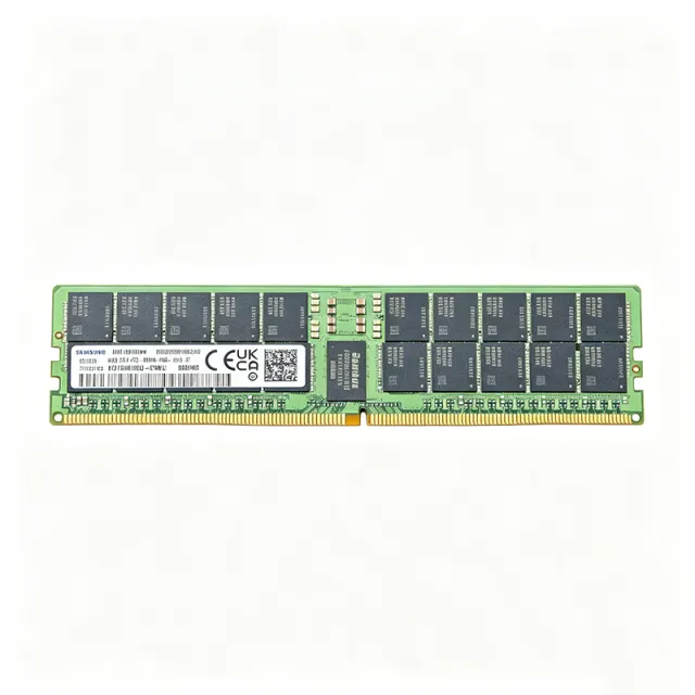
M321R8GA0EB2-CWM - 64GB DDR5-5600 ECC RDIMM | Samsung
The Samsung M321R8GA0EB2-CWM is a 64GB DDR5-5600 ECC registered DIMM (RDIMM) with dual-rank x4 (2Rx4) organization, operating at 1.1V on a 288-pin DIMM module built with Samsung D-die DRAM devices in a (4G x 4) x 40 composition. Registered (buffered) DIMMs are a class of server memory modules in which address, command, and control signals pass through a register chip before reaching the DRAM devices. This buffering reduces the electrical load on the memory controller, allowing servers and workstations to populate more DIMM slots per channel than is possible with unbuffered (UDIMM) memory. RDIMMs sit within the memory module hierarchy: DDR5 SDRAM device -> registered DIMM -> server memory -> enterprise datacenter memory subsystem. On-die ECC plus registered operation makes them mandatory in most multi-socket x86 server platforms. Key features of the M321R8GA0EB2-CWM include 5600 MT/s data rate (2800 MHz clock, PC5-44800 bandwidth class), CAS latency of CL46 at the rated speed, dual-rank x4 organization that improves server memory capacity scaling, and 1.1V operation that lowers power draw versus DDR4 RDIMMs running at 1.2V. The DDR5 architecture also moves the power management IC (PMIC) onto the module and introduces two independent 32-bit subchannels per module, improving memory bandwidth efficiency for multi-core CPUs. Technically, the module uses Samsung D-die 4G x 4 DDR5 DRAM components, 40 of which compose the 64GB (8G x 72 including ECC bits) registered module. The x4 device width combined with registered operation supports strong RAS (reliability, availability, serviceability) characteristics demanded in virtualization and database environments. On-die ECC detects and corrects single-bit errors internal to each DRAM die, while the registered interface maintains signal integrity at high slot counts. Typical applications include Dell PowerEdge, HPE ProLiant, Lenovo ThinkSystem, and Supermicro server platforms, as well as virtualization hosts, in-memory databases, and AI inference servers requiring high-capacity registered memory. Multiple identical modules should be installed in matched sets for optimal multi-channel bandwidth. When designing or upgrading, confirm platform BIOS support for DDR5-5600 RDIMMs, as many platforms default to lower speeds such as 4800 MT/s or 5200 MT/s depending on populated DIMMs per channel. Mixing module speeds causes all modules to run at the slowest common speed. This page synthesizes verified distributor specifications, drop-in alternatives, pricing context, and practical deployment notes not consolidated in the manufacturer datasheet.
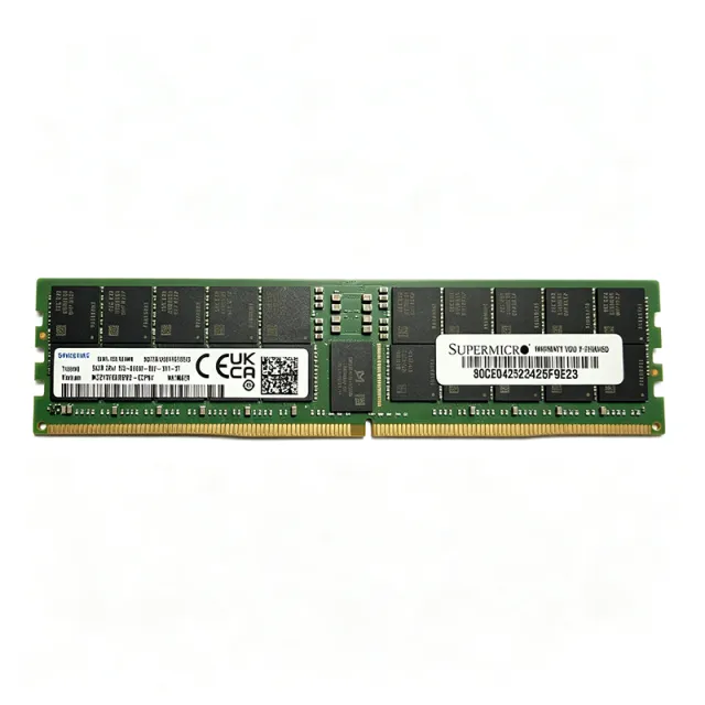
M321RYGA0PB2-CCP - 96GB DDR5-6400 ECC RDIMM | Samsung
The Samsung M321RYGA0PB2-CCP is a 96 GB DDR5-6400 ECC Registered DIMM (RDIMM) server memory module rated at 6400 MT/s (PC5-51200) with 1.1 V nominal operation, organized as 2Rx4 (dual-rank, x4 DRAM) in a 288-pin RDIMM form factor. It is built from 40 FBGA 6Gx4 DDR5 DRAM devices and delivers a 72-bit ECC data path (12GX72 organization) for enterprise servers and workstations. A Registered DIMM (RDIMM) is a server memory module that places a register (RCD) and data buffers between the DRAM devices and the memory controller, reducing electrical load on the command/address bus and enabling higher module densities and higher speeds than unbuffered DIMMs. Within the memory hierarchy, an RDIMM sits above UDIMM and SODIMM in capacity and reliability, and below LRDIMM in load reduction; it is the mainstream choice for two-socket and four-socket x86 servers. DDR5 adds on-module PMIC power management, on-die ECC, and two 32-bit subchannels per module. Key features of the M321RYGA0PB2-CCP include 96 GB capacity in a single module, 6400 MT/s transfer rate, 2Rx4 organization for maximum rank-level interleaving, ECC Registered operation for data integrity, and 1.1 V DDR5 standard voltage. The 96 GB density is achieved with non-binary 24 Gb DDR5 DRAM dies, allowing high capacity without the cost of 3DS stacking. Technically, the module uses 40 FBGA 6Gx4 DRAM packages arranged in two ranks of twenty devices each, with a 288-pin edge connector and a 72-bit ECC data path. The on-module PMIC and SPD hub are part of the JEDEC DDR5 RDIMM architecture, and the module is 100% JEDEC compliant per distributor documentation. Typical applications include enterprise rack servers, virtualization hosts, in-memory databases, and high-performance workstations where 96 GB per DIMM enables dense configurations. The 2Rx4 organization and ECC RDIMM design suit memory-bandwidth-bound workloads such as AI inference, analytics, and VDI. When designing or upgrading, verify that the server platform supports 24 Gb non-binary DDR5 DRAM and 96 GB RDIMM densities, and populate DIMMs per the vendor's population rules to maintain rated 6400 MT/s speed. This page synthesizes distributor pricing, drop-in alternatives, and practical design notes not found in the manufacturer datasheet.
M471A2G43AB2-CWE - 16GB DDR4-3200 SO-DIMM | Samsung
The Samsung M471A2G43AB2-CWE is a 16 GB unbuffered non-ECC DDR4 SO-DIMM module rated at 3200 MT/s (PC4-25600), organised as a single 1x16 GB rank in the industry-standard 260-pin SO-DIMM form factor used in laptops, mini-PCs, and small-form-factor systems. A SO-DIMM (Small Outline Dual In-Memory Module) is a compact JEDEC-standard memory module derived from the full-size DIMM but roughly half the height. DDR4 SDRAM is the fourth generation of double data rate synchronous DRAM; it operates at lower voltage (1.2 V) than DDR3 (1.5 V), reaches higher per-pin data rates up to 3200 MT/s at launch, and uses a 288/260-pin edge connector with point-to-point topology. The SO-DIMM variant mounts vertically in laptop sockets and supports up to 2 ranks per module (2DPC in some platforms). Key features include 16 GB density in a 1Rx8 organisation (built from sixteen 1 Gx8 FBGA-78 die), 3200 MT/s transfer rate (PC4-25600), CAS Latency 22 (CL22), 1.2 V typical operating voltage (1.14-1.26 V per JEDEC DDR4 spec), and JEDEC-compliant 260-pin SO-DIMM edge finger geometry. The module is unbuffered, non-ECC, and supports standard SPD timings for plug-and-play compatibility with Intel and AMD mobile platforms. Technically, the module follows the JEDEC DDR4 standard JESD79-4, supporting on-die termination (ODT), command/address parity on qualified platforms, and write CRC for signal-integrity robustness. The 1Rx8 organisation routes a single 64-bit data word through eight x8 DRAM devices per rank, balancing density and signal loading for mobile workloads. Typical applications include laptop memory upgrades, ultrabook and thin-client RAM expansion, mini-PC and small-form-factor workstations, and embedded industrial PCs that require JEDEC-standard SO-DIMM compatibility. The 3200 MT/s rating aligns with mainstream 11th/12th-generation Intel Core and AMD Ryzen mobile platforms. Design consideration: when populating two SO-DIMM sockets, mixing 1Rx8 and 2Rx8 modules downgrades the channel to the slower rank's timings on some chipsets - use matched modules for dual-channel performance. This page synthesises distributor pricing, JEDEC-aligned specifications, drop-in alternatives, and practical upgrade notes not always shown on a single distributor listing.

M48T02-70PC1 - 5V 16Kbit TimeKeeper SRAM RTC | STMicroelectronics
The STMicroelectronics M48T02-70PC1 is a 5.0 V, 16 Kbit (2 Kb x 8) non-volatile TimeKeeper SRAM that integrates an ultra-low-power SRAM, a real-time clock (RTC), and a power-fail control circuit in a single 24-pin DIP Module package (0.600 inch / 15.24 mm). The device is pin and function compatible with the JEDEC-standard 2 Kb x 8 SRAM footprint, allowing direct replacement of a parallel SRAM while adding battery-backed timekeeping. Access time is 70 ns, matching common asynchronous SRAM timing requirements. The on-board lithium coin cell provides a minimum of 10 years of data and clock retention in the absence of external power across the operating temperature range. A real-time clock (RTC) is a dedicated integrated circuit that tracks seconds, minutes, hours, days, dates, months, and years with automatic leap-year compensation. The M48T02 family combines RTC functionality with a non-volatile static RAM, forming a TIMEKEEPER (utility) hybrid module that retains data and time without external backup hardware. Such modules sit in the system hierarchy as Memory ICs > Non-volatile SRAM > RTC + SRAM combination modules, and are widely used when a host MCU needs both configuration storage and wall-clock time across power cycles. Key features include a parallel address/data bus interface (multiplexed to match a standard 2K x 8 SRAM pinout), BCD-formatted clock registers, automatic leap-year correction through 2099, programmable square-wave output, and built-in power-fail write protection that locks the SRAM when VCC drops below the lithium backup threshold. The TIMEKEEPER (utility) architecture means the user simply reads and writes the SRAM address space - clock information is mapped into the upper RAM addresses - so existing SRAM software drivers work with no modification. Typical applications include industrial controllers, point-of-sale terminals, data loggers, metering equipment, security and access-control systems, and any embedded design that needs both battery-backed parameter memory and a calendar-clock. Designers should observe the VCC power-up ramp specifications in the datasheet to ensure the battery switchover circuit latches correctly, and avoid applying external bias to the backup cell. The through-hole DIP-24 module remains popular for legacy boards, prototypes, and field-replaceable designs where socketed parts are desirable.

M48T58-70PC1 - 64Kbit Timekeeper SRAM RTC 70ns | STMicroelectronics
The STMicroelectronics M48T58-70PC1 is a 5.0 V, 64 Kbit (8 Kb x 8) non-volatile Timekeeper SRAM that integrates an 8 Kb x 8 static RAM, a real-time clock, a power-fail control circuit, and a lithium battery in a single 28-pin DIP Module package. It provides 70 ns access time and operates over a 4.75 V to 5.5 V supply range, delivering a battery-backed-up memory and real-time clock solution in one footprint. A Timekeeper SRAM is a hybrid non-volatile memory device that combines the byte-wide random access of a standard SRAM with on-chip battery backup and an integrated real-time clock. It belongs to the broader family of non-volatile RAM (NVRAM) products, sitting between conventional SRAM and serial NVSRAM/FRAM in the memory hierarchy. Compared to standard SRAM, a Timekeeper eliminates external battery-management circuitry and supports BCD-coded year/month/day/date/hour/minute/second read-out. Key features include 70 ns read/write access time, integrated lithium battery with typical 10-year data retention, automatic power-fail/write-protection circuitry, bytewide RAM-like clock access, BCD-coded year/month/day/date/hour/minute/seconds registers, frequency test output for real-time clock, and JEDEC-standard 8 K x 8 SRAM pin/function equivalence. The monolithic chip ships in a special 28-pin DIP Module (CAPHAT) that accommodates the embedded battery cell. The architecture centers on a low-power 8K x 8 SRAM array, a 32 kHz crystal-controlled oscillator for the RTC, and a power-fail comparator that latches the CS/WE/OE write-protect signals when VCC drops below a defined threshold. The internal lithium cell then holds both the SRAM contents and the RTC registers, allowing the device to drop into any JEDEC-standard 8K x 8 SRAM socket without any WRITE-timing constraints. Typical applications include industrial data logging, point-of-sale terminals, metering equipment, factory automation controllers, medical instruments, and any embedded system that requires both non-volatile variables and a wall-clock/calendar without an external backup battery or RTC chip. Designers use it as a one-chip substitute for SRAM + discrete RTC + supercapacitor/cell combinations. When designing with this device, observe the standard 8K x 8 SRAM timing (address setup, CS-to-OE, write-pulse width) and route the VCC decoupling close to the supply pin. Because the lithium cell is non-replaceable in the CAPHAT package, treat the module as a sealed unit; planned end-of-life data retention after VCC removal is on the order of 10 years per the manufacturer. This page synthesizes distributor pricing, verified drop-in alternatives, and practical design notes that go beyond the manufacturer's datasheet, supporting faster component evaluation.

M58BW32FB5T3F - 32Mbit 3.3V NOR Flash, 55ns | Micron
The Micron Technology M58BW32FB5T3F is a 32Mbit parallel NOR Flash memory IC organized as 1M x 32 bits, operating from a single 3.3V supply with a 55 ns access time, housed in an 80-pin PQFP (14x20 mm) package. It is the automotive-grade variant of the M58BW32F family, qualified to AEC-Q100 for use in vehicular and harsh-environment electronic systems. A parallel NOR Flash memory is a nonvolatile semiconductor memory in which memory cells are connected in parallel, allowing random access to any address directly. In the memory hierarchy, NOR Flash sits alongside DRAM, NAND Flash, and EEPROM within the broader flash memory and solid-state storage category. Unlike NAND Flash, NOR Flash supports execute-in-place (XIP), making it the standard choice for storing boot code, firmware, and parameter tables in embedded processors and microcontroller systems. Key features of the M58BW32FB5T3F include the 32Mbit (1M x 32-bit) organization on a 16-bit/32-bit parallel data bus, a fast 55 ns read access time that eliminates the need for processor wait states in many designs, and a single 3.3V supply that simplifies power rail design. The boot block architecture allows protected small sectors at the bottom of the array for reset and exception vectors, while larger sectors store application firmware. Technically, the device belongs to the 16Mb/32Mb 3.3V burst-mode parallel NOR Flash family originally developed by STMicroelectronics and later manufactured by Micron Technology. It supports asynchronous page read as well as burst read modes synchronized to an external clock, enabling high-throughput code fetch for high-performance CPUs. Standard command-set programming and block erase operations are controlled via the memory command interface, with status polled through dedicated signals. Typical applications include automotive telematics and infotainment boot storage, industrial control modules requiring firmware retention, and networking equipment storing configuration images. The AEC-Q100 qualification and temperature-grade ordering suffix (3F) target under-hood and harsh-environment deployments. Design consideration: verify burst-clock timing and wait-state configuration against the 55 ns access time, and respect the sector-erase endurance ratings in firmware update schemes. This page synthesizes distributor pricing, drop-in alternatives, and practical design notes not found in the manufacturer datasheet, with specifications verified against Micron and distributor data as of 2026-09-05.