Управление питанием
Подкатегории
Товары (2819)

AP1661MTR-G1 - 800mA PFC Controller | Diodes Incorporated
The Diodes Incorporated AP1661MTR-G1 is an active boost power-factor-correction controller rated for 0.800 A output and a 14.5 V VIN condition, supplied in an 8-pin SOIC package. The component is intended primarily as a pre-converter in electronic power supplies where correcting input-current phase and improving power factor are priorities. Its boundary-conduction-mode operation, 600 mA to 800 mA current-related ratings, and 2.5 V reference-related information identify it as a compact PFC solution rather than a conventional standalone regulator. A power-factor-correction controller is an integrated circuit that controls the switching stage of a boost converter so the input current tracks the input voltage more closely than a simple linear or rectifier circuit. In the power-management hierarchy, AP1661MTR-G1 belongs to the PFC controller class, supports a boost-converter topology, and is intended to reduce input-current distortion in AC-to-DC power supplies. Its 8-pin SOIC package is surface-mount compatible and suitable for compact power-conversion boards. Verified distributor information identifies AP1661MTR-G1 as an active, RoHS-compliant SOIC-8 device. The listed operating-temperature range is -40 °C to +85 °C. The available technical summary also reports an 800 mA IOUT condition, a 14.5 V VIN condition, boundary-conduction-mode PFC operation, 600 mA and 800 mA current ratings, a 50 µA current-related specification, and a 2.5 V reference-related specification. Other detailed electrical limits, switching frequency, protection thresholds, pin functions, and timing values are not supplied in the verified data and require the manufacturer datasheet. Typical applications include AC-to-DC front ends for industrial power supplies, server or telecom power-supply modules, adapters, chargers, and other systems where near-unity power factor can reduce reactive and harmonic current. In a practical implementation, the controller drives external MOSFETs, rectifiers, inductors, sensing resistors, and protection circuitry; it does not directly provide the final isolated output voltage. The primary design consideration is ensuring adequate voltage headroom, current sensing, switching-node layout, and thermal capacity for the external boost components. Designers should verify the exact AP1661MTR-G1 datasheet and application circuit before finalizing component values, since the supplied web data does not expose a complete pinout or full timing and electrical tables. This page consolidates verified distributor specifications, package and lifecycle information, replacement-search results, and practical design guidance for engineers evaluating AP1661MTR-G1 in power-factor-correction systems.

AP1661P-E1 - 14.5V 0.8A BCM PFC Controller | Diodes Inc.
The Diodes Incorporated AP1661P-E1 is a boundary-conduction-mode power-factor-correction controller rated for 14.5 V supply operation, 0.8 A output, and a -40°C to +85°C temperature range, supplied in an 8-DIP package. It is designed primarily as a boost pre-converter controller for power-supply systems that require active input-current shaping and improved power factor. A power-factor-correction controller is a specialized power-management IC used in the hierarchy power supply control → PFC controller → AC/DC power conversion. In a boost PFC stage, it commands a switching power stage so that input current is drawn with a shape closer to the AC input voltage. That action reduces reactive current and helps the upstream system meet harmonic and power-factor targets while charging a downstream DC bus. Verified source material identifies boundary-conduction mode, 14.5 V supply operation, 0.8 A output, -40°C to +85°C operation, an 8-DIP package, and RoHS compliance. The controller is intended for compact power-supply designs where active PFC is required, including offline AC/DC converters and boost pre-regulators. Its through-hole package supports conventional PCB assembly rather than a surface-mount land pattern. The AP1661 family is associated with a BCM operating approach, allowing the power stage to conduct for a controlled interval during each switching cycle. This can reduce switching losses compared with continuous-conduction operation over part of the operating range, although actual efficiency depends on the switch, inductor, rectifier, input voltage, output voltage, and load. The controller does not provide the complete boost converter; external power-stage components are required. A key design consideration is validating the complete PFC loop with the intended magnetics and switching components. Keep the high-current boost path compact and separate from sensitive control traces, provide suitable input and output capacitors, and verify startup, current-sense limits, gate-drive behavior, and thermal margin over the required line and load ranges. The controller’s -40°C to +85°C specification should be checked against the enclosure’s worst-case ambient temperature. This product page combines verified AP1661P-E1 specifications, sourcing information, cross-reference results, and practical engineering guidance. It distinguishes verified values from unavailable manufacturer details and does not infer pricing, pin assignments, or electrical limits that were not supplied in the source data.

AP2210K-3.3TR - 300mA RF ULDO 3.3V Fixed | Diodes Incorporated
The Diodes Incorporated AP2210K-3.3TR is a 300 mA ultra-low-dropout (ULDO) linear regulator with a fixed 3.3V output, housed in a 5-pin SOT-23 (SOT-23-5) surface-mount package. It provides very low noise, an ultra-low dropout voltage of typically 250 mV at 300 mA, very low standby current of 1 µA maximum, and excellent power supply ripple rejection (PSRR) of 75 dB at 100 Hz. A Low-Dropout (LDO) linear regulator is a type of voltage regulator that maintains a stable output voltage even when the input voltage approaches the output voltage, with the "dropout" specification being the minimum VIN-to-VOUT differential required to sustain regulation. LDOs belong to the broader hierarchy of linear regulators -> voltage regulators -> power management ICs -> semiconductors. Unlike switching converters, LDOs add no switching noise but dissipate the difference (VIN - VOUT) multiplied by load current as heat, making them preferred for noise-sensitive analog and RF rails. Key features of the AP2210K-3.3TR include CMOS process technology, individual logic-compatible enable/shutdown control input, low-power shutdown mode for extended battery life, overcurrent protection, overtemperature protection, and reversed current protection. The 3.3V fixed output is factory-trimmed, eliminating external feedback resistors and reducing the external BOM to two ceramic capacitors plus the EN bypass. The AP2210K-3.3TR uses a P-channel MOSFET pass element in a CMOS architecture, which is what enables the ultra-low quiescent current (typically 1 µA in shutdown) and the very-low reverse-leakage protection path. Its high PSRR at low audio frequencies (75 dB at 100 Hz) is particularly effective at suppressing rectified mains ripple that can otherwise couple into RF signal chains and baseband stages. The internal reference and error amplifier are trimmed at the wafer stage, so no post-package adjustment is needed for output accuracy. Typical applications include battery-powered handsets and PDAs, RF electronics, cordless phones, handheld instrumentation, portable media players, and low-power MCU supply rails. The 3.3V fixed version is a natural match for 3.3V microcontrollers, Bluetooth/Wi-Fi modules, and sensor subsystems that demand clean supply rails. When designing with this part, select ceramic input and output capacitors rated for the lowest expected operating temperature (X5R/X7R dielectric recommended), and keep the loop-trace area small to preserve phase margin. Note that this is the "TR" (tape-and-reel, non-green) packaging variant; the RoHS-compliant equivalent is AP2210K-3.3TRG1. This page synthesizes distributor stock and pricing, drop-in alternatives (including same-brand output-voltage variants and cross-brand replacements), and practical design notes not consolidated on any single manufacturer page.
AP3441SHE-7B - 3A, 1MHz Sync Step-Down DC-DC Converter | Diodes
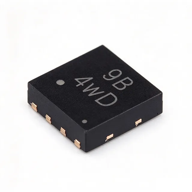
The Diodes Incorporated AP3441SHE-7B is a 3A synchronous step-down (buck) DC-DC converter with a fixed 1 MHz switching frequency and a wide 2.7 V to 5.5 V input range, housed in an 8-pin U-DFN2020-8 (UDFN-8) exposed-pad package. Per the manufacturer datasheet, the device delivers an adjustable output from 0.6 V up to VIN with ±1.5% reference accuracy and supports 100% duty-cycle operation for low-dropout conditions. The synchronous rectifier is integrated on-chip, eliminating the need for an external Schottky diode and simplifying the bill of materials. A buck (step-down) DC-DC converter is a switching regulator that efficiently reduces a higher DC input voltage to a lower DC output voltage by alternately storing energy in an inductor and releasing it into a load. Synchronous buck ICs integrate both the high-side and low-side MOSFETs, replacing the traditional rectifier diode with a low-Rds(on) MOSFET to achieve peak efficiencies above 90%. Within the broader taxonomy, AP3441 belongs to: switching regulator -> DC-DC converter -> power management IC -> semiconductor. It is purpose-built for low-voltage, high-current point-of-load (POL) conversion in portable and space-constrained products. Key features of the AP3441SHE-7B include 55 µA typical no-load quiescent current, sub-1 µA shutdown current, internal soft-start, thermal shutdown, cycle-by-cycle current limit, and constant-frequency PWM control with no required external compensation components. The high 1 MHz switching frequency enables the use of small inductors and ceramic output capacitors, shrinking the total solution footprint to roughly the size of the IC package itself. At heavy loads, the PWM control provides excellent stability and fast transient recovery; at light loads the device automatically transitions to a pulse-frequency modulation (PFM) mode to sustain high efficiency. The architecture uses a peak-current-mode control loop with internal slope compensation and an integrated synchronous MOSFET, allowing stable operation with ceramic output capacitors without ESR-related stability concerns. The exposed thermal pad on the underside of the UDFN-8 package provides a low thermal resistance path to PCB copper, sustaining the 3 A continuous output rating across the -40 °C to +85 °C operating range. Typical applications include single-cell Li+/Li-polymer battery powered systems, USB-powered devices, solid-state drives (SSD), portable media players, point-of-load conversion for FPGAs, ASICs, and DSPs, and distributed 3.3 V/5 V bus regulation in networking and consumer products. The wide input range also makes it suitable for multi-cell alkaline or NiMH battery stacks as well as standard 3.3 V and 5 V rails. When designing, select a 1 µH to 4.7 µH shielded inductor with a saturation rating above the peak inductor current (around 4 A for 3 A loads), place input/output ceramic capacitors as close as possible to the IC, and provide at least four thermal vias under the exposed pad to spread heat. To preserve efficiency, route the feedback trace away from the inductor and switching nodes. This page consolidates tier pricing, drop-in alternatives, and design notes that go beyond the datasheet to accelerate your design-in. This page synthesizes distributor tier pricing, drop-in pin-compatible alternatives, and practical PCB-layout design notes not found in the manufacturer datasheet.

AP61102Z6-7 - 1A Synchronous Buck Converter, 2.3-5.5V | Diodes
The Diodes Incorporated AP61102Z6-7 is a 1 A synchronous step-down (buck) DC-DC converter with a wide 2.3 V to 5.5 V input range and an adjustable output from 0.6 V up to 3.6 V, housed in a compact 6-pin SOT-563 / SOT-666 surface-mount package. The device integrates a 110 mΩ high-side MOSFET and an 80 mΩ low-side MOSFET, providing high-efficiency step-down conversion from common 3.3 V or 5 V supply rails to point-of-load voltages used by SoCs, MCUs, and FPGAs. A buck converter (step-down switching regulator) is a type of DC-DC converter that uses a controlled switch, an inductor, and output capacitance to deliver a lower DC voltage from a higher DC input with high efficiency. Synchronous buck converters replace the conventional Schottky rectifier with a low-side MOSFET, reducing conduction loss and improving thermal performance at moderate-to-high load currents. The AP61102 belongs to the broader hierarchy of DC-DC converters -> switching regulators -> power management ICs, sitting alongside LDOs and charge pumps in modern POL architectures. Key features include a fixed 2.2 MHz switching frequency that allows the use of small inductors and ceramic output capacitors, a Constant On-Time (COT) control architecture that delivers fast transient response, low quiescent current suitable for always-on and partial-power applications, internal soft-start, Power-Good (PG) indication, and full protection with over-current, over-voltage, short-circuit, and thermal shutdown. The 2.2 MHz switching frequency stays above the AM broadcast band, simplifying EMI filtering. The AP61102 uses Diodes' proprietary COT control topology, which eliminates the need for an external compensation network. Compared with traditional voltage-mode or current-mode buck regulators, COT delivers faster transient response to load steps and simpler external BOM with typically only an inductor and two ceramic capacitors required. Typical applications include USB Type-C / 5 V-powered IoT nodes, solid-state drives and storage modules, single-cell Li-ion battery-powered portable electronics, home automation gateways, 3.3 V POL rails for low-power MCUs, and wearables that need a small footprint and high efficiency across light and heavy loads. When designing, keep the input capacitor within 2 mm of the VIN and PGND pins to suppress switching noise, select a 1 µH to 2.2 µH shielded inductor with low DCR for best efficiency, and reserve PG for sequencing or fault monitoring in multi-rail systems. The 6-pin SOT-563 footprint is among the smallest 1 A buck footprints available. This page combines verified distributor pricing, drop-in same-package alternatives, and practical PCB design notes not consolidated in the manufacturer datasheet, giving engineers a single reference for sourcing and second-source decisions.

AP62200TWU-7 - 18V/2A Sync Buck Converter, TSOT-23-6 | Diodes Inc
The Diodes Incorporated AP62200TWU-7 is a 2A synchronous step-down buck converter accepting a wide 4.2V to 18V input range and producing an adjustable 0.8V to 7V output, housed in a 6-pin TSOT-23-6 (TSOT26) package. It integrates a 90mΩ high-side MOSFET and a 65mΩ low-side MOSFET, achieving high-efficiency DC-DC conversion at 750kHz switching frequency with PFM light-load operation. According to the Diodes AP62200 datasheet, this device targets compact point-of-load applications where small PCB footprint and high efficiency are required. A buck converter (step-down switching regulator) is a type of DC-DC converter that uses an internal high-side switch, an external inductor, and synchronous rectification to produce an output voltage lower than its input. It belongs to the switching regulator family within the power management IC hierarchy: buck converter -> switching regulator -> DC-DC converter -> power management IC -> semiconductor. Synchronous buck converters replace the external Schottky diode with an internal low-side MOSFET, dramatically improving efficiency at light loads and shrinking the solution footprint. Key features include 4.2V to 18V wide input range, 2A continuous output current, 0.8V to 7V adjustable output via external resistor divider, 750kHz switching frequency with PFM pulse-skipping at light loads, internal 90mΩ/65mΩ power MOSFETs, and built-in protection including over-current protection (OCP), over-temperature protection (OTP), and under-voltage lockout (UVLO). The TSOT-23-6 package enables designs as small as a few external passive components. The AP62200TWU-7 uses constant-on-time (COT) control architecture, providing fast transient response and simple loop compensation. Compared to traditional voltage-mode or current-mode buck converters, COT architecture requires no external compensation network, reducing BOM cost and PCB area. The integrated synchronous MOSFETs eliminate the need for an external Schottky diode, further simplifying the design and improving efficiency to peak values typically above 90% at moderate loads. Typical applications include distributed 5V/3.3V/1.8V/1.2V rails in set-top boxes, networking equipment, surveillance cameras, IoT gateways, LCD displays, and consumer electronics. The wide 4.2V to 18V input range makes the AP62200TWU-7 suitable for both 5V USB-powered systems and 12V industrial bus systems. When designing with this device, ensure the input capacitor (typically 22µF ceramic) is placed close to the IC pins and the feedback resistor divider uses 1% tolerance resistors for accurate output voltage regulation.
AP62250WU-7 - 2.5A 18V Sync Buck Converter, TSOT-23-6 | Diodes Inc.
The Diodes Incorporated AP62250WU-7 is a 2.5 A synchronous step-down (buck) DC-DC converter with a 4.2 V to 18 V input window, offered in a 6-pin TSOT-23-6 (Thin SOT-23-6) package. It integrates a 75 mΩ high-side MOSFET and a 45 mΩ low-side MOSFET, supports an adjustable output from 0.8 V to 7 V, and uses Constant On-Time (COT) control for fast transient response with a low external component count. What is a buck converter? A buck converter (also called a step-down switching regulator) is a type of switched-mode power supply (SMPS) that converts a higher DC input voltage to a lower DC output voltage with high efficiency. Buck converters sit in the hierarchy: buck converter -> DC-DC converter -> switching regulator -> power management IC -> semiconductor. They are essential in modern electronics because they deliver much higher efficiency than linear regulators, especially when the input-to-output voltage differential is large. Key features include 4.2 V to 18 V input, 2.5 A continuous output current, adjustable output from 0.8 V to 7 V, 75 mΩ high-side / 45 mΩ low-side integrated MOSFETs, low quiescent current, and internal compensation that minimizes external component count. The COT control scheme provides pseudo-fixed switching frequency with excellent line and load transient response, simplifying the FB compensation network. The COT control topology with internal compensation enables a compact PCB footprint using only a small inductor and two ceramic capacitors. The high-side and low-side MOSFETs are fully integrated, so no external Schottky diode or FET is required, which reduces BOM cost and PCB area. The wide 4.2 V to 18 V input range supports both 5 V and 12 V bus systems common in consumer, industrial, and distributed-power architectures. Typical applications include 5 V and 12 V distributed bus step-down points-of-load, set-top boxes, LCD displays, networking equipment, industrial control systems, and battery-powered portable devices where small solution size, high efficiency, and a low external component count are critical. The 2.5 A rating also makes it well-suited for powering FPGAs, SoCs, and high-current digital rails. When designing with the AP62250WU-7, select the output inductor so that ripple current falls in the 20% to 40% range of full load, and place the input/output ceramic capacitors close to the IC to minimize switching-node ringing. The FB resistor divider sets VOUT via VREF = 0.8 V; use 1% resistors for accurate regulation. This page synthesizes Diodes Incorporated datasheet specifications, current distributor pricing, drop-in cross-brand options, and practical layout/design notes that go beyond what is printed on the manufacturer's 21-page data sheet.
AP63200WU-7 - 32V 2A Sync Buck Converter | Diodes Inc | TSOT-23-6
The Diodes Incorporated AP63200WU-7 is a 2A synchronous buck (step-down) DC-DC converter with a 3.8V to 32V wide input voltage range, housed in a 6-pin TSOT-23-6 (TSOT26) package with enhanced EMI reduction. The AP63200WU-7 features an integrated 125mΩ high-side MOSFET plus a low-side synchronous rectifier, providing up to 2A continuous output current at adjustable output voltages from 1.2V up to 12V. A buck converter (also called a step-down switching regulator) is a type of switched-mode power supply (SMPS) that efficiently converts a higher DC input voltage to a lower DC output voltage by rapidly switching an inductor-based energy transfer network. Within the broader hierarchy of power management ICs, buck regulators sit alongside boost (step-up), buck-boost, and linear regulators (LDOs); they offer far higher efficiency than LDOs at large input-to-output voltage differentials because they avoid the linear-regulator I*V dropout loss, replacing it with much smaller switching losses. Synchronous buck regulators additionally replace the traditional Schottky rectifier with a low-side MOSFET, eliminating the rectifier forward-voltage drop and improving light-load efficiency. Key features of the AP63200WU-7 include low quiescent current (low-Iq) operation, integrated high-side and low-side MOSFETs (125 mΩ/typ), a fixed 500 kHz switching frequency, and enhanced EMI reduction techniques that help meet CISPR 25 / CISPR 32 EMI limits in noise-sensitive systems. The device includes internal soft-start, over-current protection (OCP), thermal shutdown, and an enable (EN) input for sequencing. The 500 kHz switching frequency allows small external L/C components while remaining outside the AM broadcast band. The AP63200 architecture uses peak-current-mode control for fast transient response and simplified loop compensation. Synchronous rectification improves efficiency up to ~88% at 12V to 3.3V / 1A, and proprietary frequency-spreading / low-EMI gate-drive techniques reduce input and switch-node ringing. A wide VIN range allows direct operation from automotive 12V/24V buses, industrial 24V rails, or USB-PD / battery sources. Typical applications include automotive infotainment and ADAS power rails, industrial 24V sensor and PLC supplies, distributed 5V/3.3V rails from a 12V or 24V bus, set-top boxes, surveillance cameras, white goods, and any compact point-of-load (POL) supply where a small TSOT-23-6 footprint and minimal external component count are required. When designing with this part, place the input ceramic capacitor (>= 4.7 uF X7R) as close as possible to the PGND/VIN pair and use a low-ESR 4.7 uF to 22 uF ceramic output capacitor. Trace the SW node with the shortest possible loop and keep the feedback divider within 5 mm of the FB pin to avoid noise pickup. This page synthesizes distributor pricing, drop-in alternatives, application context, and practical design notes not found in the manufacturer datasheet alone, delivering a one-stop engineering reference for the AP63200WU-7.
AP63201WU-7 - 2A 32V Sync Buck Converter, 22uA Iq | Diodes Inc
The Diodes Incorporated AP63201WU-7 is a 2 A continuous-output synchronous buck (step-down) DC/DC converter with a 3.8 V to 32 V wide input range, integrated 125 mΩ high-side and 68 mΩ low-side MOSFETs, and a 22 µA ultra-low quiescent current, housed in a 6-pin TSOT-26 (TSOT-23-6 Thin) package. It switches at a fixed 500 kHz with PWM at all loads and adds PFM at light load for high efficiency, while a proprietary EMI-reduction architecture spreads the switching spectrum to ease CISPR 25 / EN 55032 compliance in automotive and industrial systems. What is a synchronous buck converter? A synchronous buck is a switching voltage regulator that steps a higher DC input down to a lower regulated DC output. It replaces the conventional rectifier diode with a low-side MOSFET (the "synchronous" switch), which significantly lowers conduction losses and boosts efficiency at moderate to high loads. Synchronous buck converters are a subset of DC-DC converters within the power management IC family, and they are distinguished from LDOs by their ability to step down large input-to-outlet ratios with high efficiency (typically 85-95%) rather than dissipating the differential as heat. Key features include an adjustable output voltage down to 0.8 V with ±1% reference accuracy, internal loop compensation (18 kΩ/7.6 nF), power-good indicator, thermal shutdown, cycle-by-cycle current limit, and a hiccup-mode overcurrent that recovers once the fault is cleared. The TSOT-26 footprint measures roughly 2.9 mm × 1.6 mm with an exposed thermal pad, enabling compact point-of-load designs. The AP63201 uses peak-current-mode control with internal compensation, which simplifies the external BOM to only input/output capacitors and an inductor. Its 500 kHz switching frequency is high enough for small magnetics but low enough to keep switching losses manageable at 2 A continuous output. The 22 µA quiescent current makes it well suited to battery-powered or always-on subsystems that spend most of their time in standby. Typical applications include 24 V industrial bus step-down to 3.3 V / 5 V / 1.8 V rails, FPGA/DSP/MCU core and I/O supplies, automotive infotainment and body electronics, distributed POL converters in telecom equipment, and general-purpose 12 V-to-low-voltage conversion in appliances and consumer devices. When designing, place the input ceramic capacitor as close as possible to PVIN and PGND, keep the feedback trace away from the inductor, and use a 4-layer PCB with a solid ground plane for EMI. The exposed thermal pad must be soldered to a sufficiently large copper pour to keep junction temperature within the 150 °C shutdown limit. This page synthesizes distributor pricing, same-family Diodes variants (AP63200/AP63203/AP63205), and drop-in cross-brand alternatives from web data, alongside practical design notes not found in the manufacturer datasheet alone.
AP63203WU-7 - 2A, 32V Synchronous Buck, 3.3V Fixed Output | Diodes Inc
The Diodes Incorporated AP63203WU-7 is a 2A synchronous step-down DC-DC buck converter housed in a TSOT-23-6 thin package. It accepts a wide 3.8V to 32V input range and provides a fixed 3.3V output, integrating 125 mOhm high-side and 68 mOhm low-side MOSFETs. The device operates at a 1.1 MHz switching frequency with enhanced EMI reduction and supports continuous 2A output current. What is a synchronous buck converter? A synchronous buck (step-down) converter is a type of switching voltage regulator that uses two MOSFETs (high-side and low-side) to convert a higher DC input voltage to a lower DC output voltage. Synchronous buck designs replace the traditional Schottky rectifier with a low-side MOSFET, improving efficiency especially at high loads. Buck converters sit within the power management IC hierarchy: switching regulator > DC-DC converter > power management IC > semiconductor. They are preferred over linear regulators when VIN-VOUT differentials exceed 1-2V due to dramatically higher efficiency. Key features of the AP63203WU-7 include an ultra-low 22 uA quiescent current, 0.8V +/-1% reference voltage accuracy, fixed 3.3V output, and 1.1 MHz switching frequency. Enhanced EMI performance is achieved through proprietary switching techniques. The 1.1 MHz switching frequency enables small external LC filters. Cycle-by-cycle peak current limiting, hiccup mode short-circuit protection, and thermal shutdown provide robust fault handling. The AP63203 employs constant-on-time (COT) control architecture, delivering fast transient response without requiring external loop compensation components. The integrated MOSFETs eliminate the need for an external Schottky diode. The high-side P-channel MOSFET blocks inrush current at startup. Typical applications include industrial 24V bus distributed power systems, USB Type-C PD adapters, home automation IoT nodes, white goods control boards, and FPGA/CPLD auxiliary rails. The wide 3.8V-32V input tolerates voltage transients commonly found in industrial and PoE applications. When designing with this device, place the input capacitor (minimum 4.7 uF ceramic) as close as possible to VIN and GND pins. The output inductor (typically 2.2 uH) and output capacitor (22 uF minimum ceramic) form the FBAR network that sets ripple performance. The EN pin can be tied to VIN for automatic startup or driven by a GPIO for sequencing. This page synthesizes distributor pricing, drop-in alternatives, and practical design notes not found in the manufacturer datasheet.
AP63205WU-7 - 32V, 2A Sync Buck Converter, TSOT-23-6 | Diodes Inc
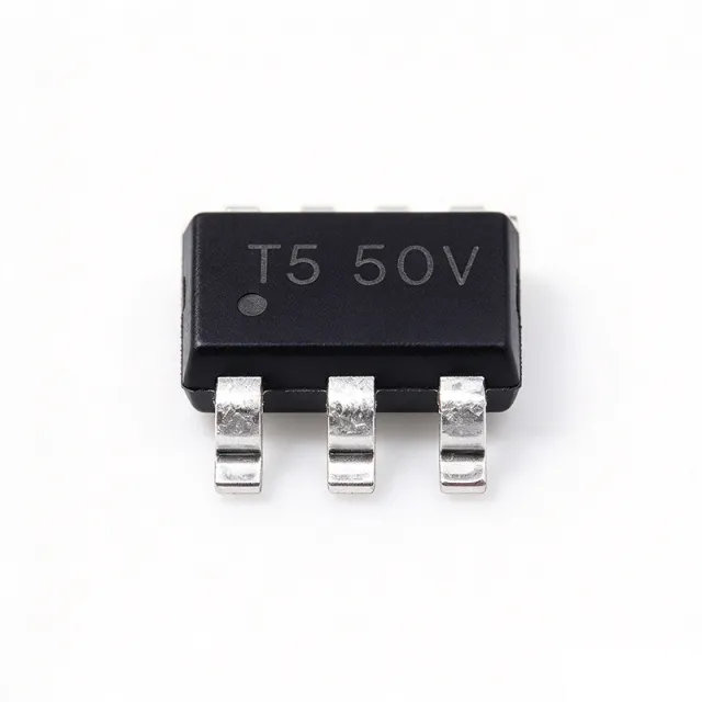
The Diodes Incorporated AP63205WU-7 is a 2 A synchronous buck (step-down) DC-DC converter with an input range of 3.8 V to 32 V and a fixed 5 V output, housed in a 6-pin TSOT-23-6 (TSOT26) package. The device integrates a 125 mΩ high-side MOSFET and a 68 mΩ low-side MOSFET for high-efficiency synchronous rectification, and switches at a nominal 1.1 MHz to enable small inductors and a minimal external component count. The fixed 5 V VOUT makes it a true drop-in point-of-load solution for the common 5 V system rail. A buck converter (also called a step-down switching regulator) is a switched-mode power supply topology that converts a higher DC input voltage to a lower DC output voltage using an inductor, a switch, and a rectifier. Within the broader power-management IC hierarchy, the buck converter belongs to the DC-DC converter family, which is a sub-category of voltage regulators and, ultimately, power management semiconductors. Synchronous versions replace the external Schottky diode with an integrated low-side MOSFET to improve efficiency, especially at light loads and at high step-down ratios. Key features include 22 µA ultralow quiescent current, 0.8 V ±1 % internal reference voltage, PWM control regardless of load, cycle-by-cycle peak current limit, and hiccup-mode overload protection. The AP63205 also incorporates proprietary EMI-mitigation techniques (frequency spread-spectrum or controlled switching-edge shaping) that simplify system compliance with CISPR 25 / EN 55022 in noise-sensitive consumer, industrial, and infotainment applications. Typical applications include 12 V to 5 V point-of-load (POL) conversion for set-top boxes, white goods, eMMC storage rails, distributed 24 V industrial-bus subsystems, USB Type-C / HDMI supply rails, always-on housekeeping supplies, and aftermarket automotive infotainment modules. The TSOT-23-6 footprint and 1.1 MHz switching frequency make it well suited for space-constrained designs that require small inductors and a clean 5 V rail. When designing with the AP63205WU-7, place the input capacitor as close as possible to the VIN and GND pins, keep the feedback trace short to minimize noise pickup, and verify that the chosen inductor saturation current exceeds the device's 2 A peak current-limit threshold. For battery-powered systems, the 22 µA Iq keeps standby drain low, but always include a bootstrap capacitor to ensure the high-side gate drive stays charged. This page synthesizes XAIPART distributor pricing, drop-in alternatives (AP63203WU-7, AP63200WU-7), comparison parameters, and practical design notes not found in the manufacturer datasheet alone.
AP63301WU-7 - 3A, 32V Sync Buck Converter, TSOT-23-6 | Diodes Inc
The Diodes Incorporated AP63301WU-7 is a 3 A synchronous buck (step-down) DC-DC converter with a 3.8 V to 32 V input range and an adjustable output from 0.8 V up to about 28 V, housed in a 6-pin TSOT-23-6 (TSOT26) package. It integrates a 75 mΩ high-side MOSFET and a 40 mΩ low-side MOSFET, supports up to 3 A continuous output current, and provides enhanced EMI reduction through an EMI-optimized gate driver architecture. Typical quiescent current is around 280 µA during light-load operation. A synchronous buck converter is a switched-mode power supply topology that uses pulse-width modulation (PWM) to regulate an output voltage lower than its input, while replacing the external Schottky diode with an internal low-side MOSFET for higher efficiency. AP63301WU-7 belongs to the hierarchy: synchronous buck converter -> buck converter -> step-down regulator -> switching regulator -> DC-DC converter -> power management IC -> semiconductor IC. This category is used wherever a board needs a low-voltage rail (e.g., 3.3 V, 5 V, 12 V) generated from a higher-voltage bus (e.g., 12 V, 24 V industrial supplies), with higher efficiency than a linear regulator. Key differentiating features include an internal high-side 75 mΩ / low-side 40 mΩ MOSFET pair, peak current-mode control with internal compensation, a 1.18 V-typical enable input that can be connected directly to VIN for automatic startup, internal soft-start, and an EMI-optimized gate driver that helps meet CISPR 25 / CISPR 22 conducted-emissions limits without complex filtering. The AP63301WU-7 is the EMI-tuned version of the family, while its sibling AP63300WU-7 adds frequency spread spectrum. Technically, the device operates at a fixed switching frequency, uses peak current-mode control for fast transient behavior and simple loop compensation, and provides cycle-by-cycle current limit, thermal shutdown, and over-voltage protection. The TSOT-23-6 package with an exposed thermal pad keeps junction-to-ambient resistance low enough for 3 A operation at moderate VIN-VOUT differentials without external heatsinking. Typical applications include 12 V and 24 V industrial bus point-of-loads, USB-PD / Type-C charging rails, white goods and home appliance power, telecom 5 V/3.3 V auxiliary supplies, and FPGA/MCU core or I/O rails. Compared with linear regulators, AP63301WU-7 dramatically lowers the heat dissipated when stepping 24 V to 5 V at 3 A. Designers should size the input capacitor for RMS current, select the output inductor for approximately 20-40% ripple, and follow the datasheet feedback-resistor table to program the output between 0.8 V and roughly VIN minus losses. This page synthesizes distributor pricing, drop-in TSOT-23-6 alternatives, and practical design notes not found in the manufacturer datasheet alone.

AP64100SP-13 - 40V 1A Sync Buck DC-DC Converter | Diodes Inc
The Diodes Incorporated AP64100SP-13 is a 1A synchronous buck (step-down) DC-DC converter with a wide 3.8V to 40V input range, 0.8V adjustable output, and an integrated 150 mΩ high-side / 80 mΩ low-side MOSFET pair, packaged in an 8-pin SOIC with exposed pad (SO-8EP). It uses peak current-mode control for fast transient response and simplified loop compensation, and operates at an adjustable switching frequency up to 2.2 MHz to keep passive components small. A buck converter (also called a step-down switching regulator) is a DC-DC topology that uses a power switch, an inductor, and a rectifier to convert a higher input voltage into a lower output voltage with high efficiency, typically 85-95%. The AP64100 belongs to the synchronous buck family, meaning it replaces the conventional Schottky diode with a low-side MOSFET, eliminating diode conduction loss. This places it within the broader hierarchy of switching voltage regulators -> DC-DC converters -> power management ICs -> semiconductors. Key features of the AP64100SP-13 include a 22 µA typical quiescent current suitable for battery-powered or always-on systems, internal compensation that removes the need for an external compensation network, programmable soft-start via an external capacitor, and a power-good indicator for sequencing. The SO-8EP package provides a low thermal resistance path through the exposed pad, supporting full 1A output at elevated ambient temperatures with minimal PCB copper area. Technically, the device uses peak current-mode control with internal slope compensation, providing cycle-by-cycle current limit and inherent input-voltage feed-forward. The high-side MOSFET RDSon of 150 mΩ (typical) and low-side 80 mΩ (typical) keep conduction losses low at 1A, while the 40V absolute maximum input voltage offers significant transient headroom for 12V and 24V industrial buses. Typical applications include 12V/24V distributed power rails in industrial automation, smart-meter and HVAC controllers, white goods and appliance subsystems, battery-powered portable equipment, eMMC/SSD storage rails, and general-purpose 5V/3.3V point-of-load conversion. Its 40V input tolerance makes it especially attractive in 24V industrial environments where voltage transients on the bus can exceed nominal levels. When designing with the AP64100SP-13, place the input bypass capacitor as close as possible to the PVIN and PGND pins, and use a continuous ground plane under the exposed pad for thermal dissipation. The feedback resistors should use 1% tolerance to maintain output voltage accuracy; the soft-start capacitor value sets the inrush current profile and should be sized to avoid triggering the UVLO threshold during startup. This page synthesizes distributor pricing, drop-in alternatives, and practical design notes not found on the manufacturer datasheet alone, providing engineers with a single source for component evaluation, sourcing, and design-in.
AP64352SP-13 - 3.5A 40V Sync Buck Converter | Diodes Inc
The Diodes Incorporated AP64352SP-13 is a 3.5A synchronous step-down (buck) DC-DC switching regulator with a wide 3.8V to 40V input range, housed in an 8-pin SO-EP (SOIC-8 with exposed pad) package. It features adjustable output from 0.8V up to 39V, integrated 75mΩ high-side and 45mΩ low-side power MOSFETs, and low quiescent current operation. The part is offered in -13 tape-and-reel packaging. A buck converter (step-down switching regulator) is a type of switched-mode power supply (SMPS) that efficiently converts a higher DC input voltage to a lower DC output voltage. It belongs to the broader hierarchy: buck converter -> DC-DC converter -> switching regulator -> voltage regulator -> power management IC -> semiconductor. Compared to linear regulators, buck converters achieve much higher efficiency (often >90%) by rapidly switching the input voltage through an inductor, rather than continuously burning excess voltage as heat. The synchronous variant uses a MOSFET in place of the conventional Schottky rectifier, further improving efficiency at high load currents. Key features of the AP64352SP-13 include its wide 3.8V-40V input range suitable for 12V/24V industrial buses, 3.5A continuous output current capability, programmable switching frequency, internal compensation that minimizes external component count, peak current mode control for fast transient response, and integrated soft-start for controlled inrush. The exposed thermal pad on the SOIC-8 package provides a low-resistance path for heat dissipation. Architecturally, the device uses peak current mode control with internal compensation, simplifying loop design and eliminating the need for external compensation components. The 75mΩ/45mΩ integrated MOSFETs reduce both BOM count and PCB footprint, while proprietary light-load management maintains high efficiency across the entire load range. The internal reference is trimmed to 0.8V ±1% for accurate output regulation. Typical applications include distributed power systems, home appliances, white goods, flat-panel TV power, audio systems, network systems, and general-purpose 12V/24V industrial point-of-load (POL) conversion. The wide input range also makes it well-suited for automotive aftermarket and eMobility applications operating from multi-cell battery stacks. When designing with the AP64352SP-13, place the input ceramic capacitor as close as possible to the PVIN and PGND pins to minimize switching noise. The exposed pad must be soldered to a sufficient copper pour (recommended at least 1 square inch) to dissipate heat and provide electrical ground. This page synthesizes distributor pricing, drop-in alternatives, and practical design notes not found on generic component search engines, giving engineers a single source for parametric, application, and sourcing decisions on the AP64352SP-13.

AP7345D-3333RH4-7 - Dual 300mA LDO 3.3V/3.3V X2-DFN1612-8 | Diodes Inc.
The Diodes Incorporated AP7345D-3333RH4-7 is a dual-channel, fixed-output CMOS LDO (Low-Dropout) linear regulator delivering 3.3V at 300mA on each of its two outputs from a single input, housed in a compact 8-pin X2-DFN1612-8 package with an exposed thermal pad. An LDO (Low-Dropout) linear regulator is a type of voltage regulator that maintains a stable output voltage even when the input voltage approaches the output voltage, with dropout voltages typically a few hundred mV. LDOs sit within the broader power management IC hierarchy, above which are switching converters and battery management ICs; LDOs are favored in noise-sensitive rails because, unlike switchers, they introduce no switching ripple into the output. The AP7345D family is specified with high PSRR, low output noise, and low quiescent current, making it ideal for primary-cell-powered systems such as those running from alkaline AA or AAA cells. Each rail is enabled independently, and the chip integrates short-circuit current limit and thermal shutdown protection. The CMOS process delivers a low RDSON pass element that minimizes dropout loss and extends battery life. The two 300mA outputs share the same 3.3V fixed voltage in the -3333RH4-7 variant; the -3333 suffix denotes a 3.3V/3.3V fixed combination. The exposed-pad X2-DFN1612-8 package measures approximately 1.6mm x 1.2mm and offers a thermal path suitable for handheld and IoT power budgets. Enable pins allow individual rail sequencing for multi-supply MCUs and wireless SoCs. Typical applications include portable consumer electronics, IoT sensors and wearables, BLE/Zigbee module supplies, single-cell Li-ion post-regulation rails, microcontroller core and RTC power, and battery-powered measurement devices. Designers often pair the AP7345D with a preceding buck regulator to step down from a USB or 1S Li-ion source before the LDO cleans up the rail. When designing with the AP7345D, place the 1uF ceramic input and output capacitors as close to the pins as possible and use low-ESR X5R/X7R dielectrics to maintain loop stability. Because each output is rated 300mA, ensure that the sum of both loads does not push the package above its thermal limit; in most battery-powered uses, the 300mA per-rail limit is the binding constraint rather than dissipation. This page synthesizes distributor pricing, drop-in same-package alternatives within the AP7345D family, and PCB layout notes not found in the manufacturer datasheet, giving engineers a faster sourcing decision than distributor catalog listings.

AP7350-30CF4-7 - 150mA 3V Ultra-Low IQ LDO | Diodes Inc
The Diodes Incorporated AP7350-30CF4-7 is a 150 mA CMOS low-dropout (LDO) linear regulator with a fixed 3.0 V output, housed in a 4-ball X2-WLB0606-4 wafer-level chip-scale package. It features an ultra-low quiescent current of 0.25 µA typical, an enable pin for power sequencing, and operates from an input voltage of up to 5.25 V with sub-300 mV dropout at full load. An LDO (low-dropout) linear regulator is a type of voltage regulator that maintains a stable output voltage even when the input-to-output voltage differential is very small. LDOs belong to the broader hierarchy of linear regulators, which in turn are a subset of voltage regulators and ultimately power management ICs (PMICs). Unlike switching converters, LDOs dissipate excess energy as heat, making them ideal where low noise, small footprint, and minimal external part count outweigh efficiency concerns. Key differentiating specifications of the AP7350-30CF4-7 include: 0.25 µA typical quiescent current (extend battery life in always-on rails), high output voltage accuracy of ±1% across line/load/temperature, integrated active-high enable for sleep-mode gating, and built-in short-circuit and thermal protection. The CMOS process enables a tiny quiescent current that is orders of magnitude lower than bipolar LDOs in the same load class. Architecturally, the AP7350 uses a CMOS pass element paired with a precision bandgap reference and feedback loop, delivering clean, low-ripple regulation without the high-frequency noise that switching regulators generate. The X2-WLB0606-4 wafer-level package (0.6 mm × 0.6 mm × 0.4 mm height) is one of the smallest LDO footprints in the industry, allowing the regulator to fit beside an IC pad rather than under it. Typical applications for the AP7350-30CF4-7 include wearable fitness bands, BLE beacons, IoT sensor nodes, hearing aids, and battery-powered data loggers. The 3.0 V fixed output is well-matched to Li-ion chemistries (3.0 V mid-discharge) and to low-power MCUs that operate from a 2.7–3.6 V supply such as the M0+ class. When designing with this device, add a 1 µF X7R ceramic input/output capacitor and route the EN pin to the host MCU GPIO so that the regulator can be placed in 0.25 µA Iq shutdown between active windows. Keep input trace inductance low to preserve load-transient response. This page synthesizes distributor pricing (LCSC, Heisener, DigiKey, Mouser), drop-in pin-compatible alternatives in the same X2-WLB0606-4 footprint, and practical design notes not found in the manufacturer's datasheet.

AP7365-SNG-7 - 600mA, Low IQ LDO, Adj 0.8V-5V, U-DFN2020-6 | Diodes Inc
The Diodes Incorporated AP7365-SNG-7 is a 600 mA low-dropout (LDO) linear regulator with an adjustable output range of 0.8 V to 5 V and a 2 V to 6 V input range, housed in a compact 6-pin U-DFN2020-6 exposed-pad package. It delivers 65 dB PSRR at 1 kHz, 600 mV dropout at 600 mA, and only 35 µA quiescent current, with built-in over-current, short-circuit, and thermal-shutdown protection. Operating temperature spans -40°C to +85°C. A low-dropout (LDO) regulator is a type of linear voltage regulator that maintains a stable output even when the input voltage approaches the output voltage. LDOs sit within the broader family of linear regulators, which are themselves a subset of voltage regulators and the parent power-management IC (PMIC) category. Unlike switching regulators, LDOs do not introduce switching noise, making them preferred for noise-critical rails in mixed-signal systems. Key features of the AP7365-SNG-7 include its 600 mA continuous output capability, low 35 µA quiescent current that preserves battery life, 65 dB PSRR at 1 kHz for ripple rejection from upstream converters, and a fixed soft-start characteristic that prevents input current surges during turn-on. The exposed thermal pad (EP) on the bottom of the U-DFN2020-6 package enhances heat dissipation and enables higher sustained current without a heatsink. The AP7365-SNG-7 uses a P-channel MOSFET pass element, which is the architectural choice that allows the very low 35 µA quiescent current (PNP-based LDOs typically draw 1-10 mA). The trade-off is slightly higher dropout voltage versus an N-channel architecture with a charge pump, but in most 3.3 V or 5 V rail applications this dropout is comfortably met. Typical applications include single-cell lithium-ion battery-powered portable electronics, USB peripherals, wireless sensor nodes, IoT edge devices, and post-regulation stages following DC-DC converters where a clean, low-noise rail is required. When designing with this device, place 1 µF ceramic input and output capacitors as close to the IC as possible, choose X5R or X7R dielectric for stable temperature performance, and use the exposed pad to drop thermal resistance to approximately 60°C/W on a 1 oz copper pour. This page consolidates drop-in cross-references, side-by-side parameter comparison tables, and engineer-level application notes that go beyond the manufacturer datasheet alone.
AP7370-33W5-7 - 300mA, 3.3V Fixed ULDO Regulator | Diodes Inc
The Diodes Incorporated AP7370-33W5-7 is a 300 mA ultra-low-dropout (ULDO) linear regulator with a fixed 3.3 V output, housed in a 5-pin SOT-25 surface-mount package. Designed for wide input operation from 3.2 V to 18 V, it delivers high-accuracy regulation with low dropout, current-limit protection, reverse-current protection, and ultra-low quiescent current. An LDO (Low-Dropout) linear regulator is a type of voltage regulator that maintains a stable output voltage even when the input voltage is very close to the output voltage, dissipating only the difference (VIN - VOUT) multiplied by load current as heat. The AP7370 belongs to the ULDO sub-family — regulators optimized for sub-100 mV dropout at full load — and sits inside the broader hierarchy of linear regulators, voltage regulators, power-management ICs, and semiconductors. Key features of the AP7370-33W5-7 include a fixed 3.3 V ±1% output accuracy, typically 200 mV dropout at 300 mA load, current-limit fold-back protection, reverse-current blocking when the input falls below the output, and ultra-low quiescent current for always-on battery applications. The SOT-25 package measures approximately 2.9 mm × 1.6 mm, with a thermal pad that lowers θJA and enables 300 mA continuous output in compact industrial, USB, and portable-device designs. The architecture uses a PNP pass element driven by a precision bandgap reference and error amplifier. The wide 3.2 V-to-18 V input range lets the regulator accept 5 V, 9 V, 12 V, and 15 V rails directly without a pre-regulator, simplifying USB-powered, 12 V wall-adapter, and multi-cell battery designs. Reverse-current protection guards against back-feeding when VOUT exceeds VIN during plug-in events. Typical applications include USB-powered devices, portable instrumentation, microcontroller and MCU-rail supplies, battery-powered IoT nodes, point-of-load regulation after a switching converter, and industrial sensor modules. Always-on rails in metering and remote-monitoring equipment benefit from the part's sub-µA quiescent current. When designing with the AP7370-33W5-7, place a 1 µF or larger low-ESR ceramic input capacitor close to VIN and a 1 µF ceramic output capacitor close to VOUT. Observe the absolute maximum input voltage of 20 V and derate output current above +85 °C. The EN logic is fixed-on in the -33 variant; if shutdown control is needed, refer to the AP7370-12/15/18/25/28/30 fixed-voltage siblings or pin-compatible ULDO alternatives. This page synthesizes distributor pricing, drop-in alternatives, and practical design notes not found in the manufacturer datasheet.
AP7370-33WR-7 - 300mA, 18V Wide-Input ULDO Regulator, 3.3V Fixed | Diodes Inc
The Diodes Incorporated AP7370-33WR-7 is a 300 mA positive fixed-output ultra-low-dropout (ULDO) linear regulator delivering a factory-set 3.3 V output from a wide 3.6 V to 18 V input range in a 5-pin SOT-25 package. The part is supplied on a 7-inch 3,000-piece reel (suffix -7) and targets USB-powered, portable, battery-backed, and instrumentation applications where high accuracy, low quiescent current, and reverse-current protection are required. A Low-Dropout (LDO) linear regulator is a type of voltage regulator which can maintain a stable output voltage even when the input voltage is only marginally higher than the output. LDOs sit one layer below generic linear regulators in the power management hierarchy (LDO -> linear regulator -> voltage regulator -> power management IC), and unlike switching converters they generate no switching noise, trading place for either north of 5V dropout even at small VIN-VOUT deltas. Key features of the AP7370 include a typical quiescent current of just a few microamperes, an enable pin for power sequencing, integrated current limit and thermal-shutdown protection, and reverse-current blocking for safe operation into pre-biased outputs. Output accuracy is trimmed at the factory to within a few percent of the 3.3 V nominal output, making it suitable as a clean post-regulator after switching converters in mixed-rail systems. The device uses a low-resistance internal P-MOSFET pass element and is internally compensated, so a small ceramic output capacitor is sufficient for stability. The SOT-25 footprint plus wide input tolerance allow the part to drop directly into industrial 12 V/15 V bus designs, USB rails, and point-of-sale targets, replacing discrete transistor-based regulators with a single 5-pin IC. Typical applications include USB-powered devices, portable instrumentation, MCU/FPGA sense rails in 12 V systems, battery chargers, and battery management systems. The fixed 3.3 V variant is a particularly good fit for low-power microcontrollers and Bluetooth/Wi-Fi modules that require a clean post-regulator from a higher bus battery. When designing with this part, ensure that the input-to-output differential never exceeds the absolute maximum rating; this is especially important in industrial 24 V systems where input transients can momentarily exceed the absolute maximum. A small input ceramic bypass capacitor placed close to the VIN pin is recommended, and the exposed tab (if used for heat spreading) must be soldered to a sufficient copper pad. This page aggregates distributor pricing, drop-in alternatives, and practical design notes not found in a single source, giving engineers a one-stop comparison reference for the AP7370 family.
AP7370-50W5-7 - 300mA, 18V, 5V Fixed ULDO Regulator | Diodes Inc
The Diodes Incorporated AP7370-50W5-7 is a 300 mA, fixed 5.0 V output, ultra-low-dropout (ULDO) linear voltage regulator in a 5-pin SOT-25 package, designed for wide-input battery-powered and USB applications. According to the Diodes Incorporated datasheet, it accepts a wide input voltage range up to 18 V (typical operating maximum), maintains regulation with a dropout of roughly 500-550 mV at 100 mA, and consumes only about 2.5 µA of quiescent current, extending battery life in always-on systems. The output is factory-trimmed to 5.0 V and delivered through a 300 mA N-channel MOSFET pass element that yields a low dropout figure without the cost of a P-channel architecture. An LDO (low-dropout) linear regulator is a type of voltage regulator that maintains a stable output voltage even when the input voltage is only slightly higher than the output - the dropout voltage is the minimum VIN-VOUT headroom required for regulation. LDOs are a subset of linear regulators, which in turn belong to the broader family of voltage regulators and power management ICs (PMICs). Unlike switching regulators, LDOs introduce no switching noise, making them the preferred choice for post-regulation after a switching converter, or as a stand-alone rail for noise-sensitive analog/RF loads. Key features of the AP7370-50W5-7 include ±2% output voltage accuracy, integrated short-circuit current limit, thermal shutdown, and reverse-current protection that prevents current backflow when the input rail collapses below the output. The device operates over a -40 °C to +125 °C junction temperature range, is rated to a maximum junction temperature of +150 °C, and is qualified to the JEDEC JESD22-A114 power-cycling and MSL-1 moisture-sensitivity levels. The SOT-25 footprint occupies roughly 2.9 mm × 1.6 mm of board area, making the part one of the densest 300 mA ULDOs available in this voltage class. The AP7370-50W5-7 is built on a CMOS process and uses a bandgap reference trimmed at wafer level. Its 2.5 µA quiescent current is among the lowest in the 300 mA / 5 V fixed class, and reverse-current protection eliminates the need for an external blocking diode when the part is powered from a USB rail that may be removed while the output capacitor holds charge. The output capacitor requires only a small ceramic (1 µF X7R is sufficient per the datasheet), simplifying BOM and reducing PCB area versus LDOs that need bulk tantalum or aluminum-polymer capacitors. Typical applications include USB-powered devices, battery packs, smart meters, IoT sensor nodes, portable instrumentation, and standby rails in consumer electronics where standby current must remain below 5 µA. The wide 18 V input tolerance also makes it well suited to 12 V industrial bus rails and to post-regulation downstream of a buck converter. When designing with this device, place the 1 µF ceramic input and output capacitors as close as possible to the IC pins to ensure loop stability, and verify that worst-case VIN-VOUT × IOUT stays within the SOT-25's thermal limits - for example, at VIN = 12 V, VOUT = 5 V, IOUT = 300 mA, the package must dissipate 2.1 W, which requires thermal copper pours. This page synthesizes distributor pricing, SOT-25 drop-in alternatives (notably the TI TPS70950QDBVRQ1 used as a confirmed drop-in by mass-production designs), and practical thermal and PCB-layout notes that are not found together in the manufacturer datasheet.

AP7383-33Y-13 - 3.3V 150mA Ultra-Low Iq LDO | Diodes Inc
The Diodes Incorporated AP7383-33Y-13 is a fixed 3.3 V positive-output ultra-low-dropout (LDO) linear voltage regulator rated at 150 mA continuous output current in a SOT-89-3 (Y package) surface-mount package. It accepts a wide input voltage range up to 30 V, features a low dropout voltage, high output accuracy, integrated current limit, and ultra-low quiescent current, which makes it ideal for always-on and battery-powered applications. The fixed 3.3 V variant (suffix -33) eliminates external feedback resistors and simplifies BOM cost. An LDO (Low-Dropout) linear regulator is a type of voltage regulator that maintains a stable, low-ripple output voltage even when the input voltage approaches the output voltage. LDOs sit within the broader power management IC hierarchy: linear regulator -> voltage regulator -> power management IC -> semiconductor. Unlike switching converters, LDOs do not generate EMI switching noise, which is essential for USB, audio, and instrumentation supplies. The AP7383's ultra-low Iq extends battery standby time in IoT and portable devices. Key features of the AP7383-33Y-13 include up to 30 V wide input voltage range, low dropout at 150 mA, internal current limit protection, thermal shutdown, and ultra-low quiescent current. The high-accuracy output (typically ±2%) supports powering MCUs, sensors, and analog/RF blocks without additional regulation stages. The SOT-89-3 package provides good thermal performance for its small footprint via an exposed tab, enabling up to 150 mA continuous load without external heatsinking. The AP7383 family uses a low-Iq CMOS architecture with an internal bandgap reference. The wide VIN tolerance (up to 30 V) allows the same part to derive a 3.3 V rail directly from industrial 24 V buses, USB VBUS, or 5 V system rails with substantial transient headroom. The integrated current limit and thermal shutdown form a robust fault envelope for harsh USB-charging or hot-plug scenarios. Typical applications include USB peripherals and chargers, portable/battery-powered devices, instrumentation, IoT sensor nodes, and post-regulation after a switching converter. The wide VIN tolerance makes the AP7383 well suited to industrial 24 V systems stepping down to 3.3 V logic rails. Always-on microcontrollers and wireless MCUs in remote or solar applications benefit from the ultra-low quiescent current. When designing with this part, ensure input and output capacitors are placed as close as possible to the pins and the exposed thermal tab is soldered to sufficient copper pour (typically >= 100 mm^2 of 1-oz copper) to dissipate heat at the rated 150 mA load. Avoid exceeding the absolute maximum input voltage during hot-plug events; add TVS protection on USB VBUS inputs that may see surge transients. This page synthesizes distributor pricing, drop-in pin-compatible alternatives, and practical PCB design notes not found on the manufacturer datasheet alone. Engineers can use the comparison_table to evaluate same-package drop-in options, and the design_notes section provides actionable guidance on capacitor sizing and thermal copper area for reliable operation up to the rated 150 mA load.
APW8706A - 25V 6A DrMOS Power Module | ANPEC
ANPEC APW8706A is a high-performance, high-current DrMOS power module with a 4.5 V to 25 V VIN range, 6 A continuous output current, 8 A peak current, and operation up to 1.5 MHz. It is supplied in the exact package identified as [DATA_NEEDED: package]. The module integrates a high-side N-channel MOSFET and a low-side N-channel MOSFET with adaptive dead-time control. A DrMOS power module is an integrated driver-and-switch-stage device used in high-efficiency DC-DC conversion. It combines power switching elements with control functions in one package, helping reduce external components and simplify synchronous buck, half-bridge, and related converter layouts. The APW8706A belongs to the MOSFET driver and power-management semiconductor hierarchy. The documented features include 4.5 V to 5.5 V operation for VCC and PVCC, adjustable over-current protection, a power-on-reset function monitoring the VCC pin, and a built-in tri-state PWM input. Adaptive dead-time control supports controlled transitions between the integrated high-side and low-side devices, while PWM operation up to 1.5 MHz permits a broad converter design range. The APW8706A is suited to compact, high-current switching systems where integrated high-side and low-side MOSFETs simplify power-stage construction. Its 6 A continuous and 8 A peak output-current ratings are particularly relevant to notebook, computing, graphics, and other compact power-conversion systems, subject to thermal and layout constraints. Designers should account for the difference between VCC/PVCC and VIN supplies, validate the power stage across its full operating range, and provide thermal copper and low-inductance switching paths. The exact package dimensions, pinout, exposed-pad arrangement, switching-loss data, and recommended land pattern are not provided in the verified data and must be checked against the manufacturer datasheet before PCB release.

AS1108WL - 4-Digit LED Display Driver, SPI/QSPI, 20-SOIC
The ams-OSRAM AS1108WL is a compact 4-digit 7-segment LED display driver that integrates a BCD Code-B/HEX decoder and a high-speed SPI/QSPI/Microwire-compatible serial interface, delivered in a 20-pin SOIC wide-body package. The IC combines constant-current segment drivers, individual LED segment control, segment blinking with multi-device synchronization, and a low-power shutdown mode in a single chip, reducing microcontroller GPIO usage while driving up to four 7-segment digits or a 4x8 dot-matrix LED panel. A 7-segment LED display driver is an interface IC that translates a microcontroller's serial or parallel data into the seven segment lines (plus decimal point) required to render numeric or alphanumeric characters on LED displays. The AS1108WL belongs to the LED display driver sub-category of display drivers, which in turn fall under power management ICs (PMIC) and interface ICs; it converts low-voltage logic-level serial data from a host MCU into multiplexed, current-regulated outputs that directly sink or source the high currents needed by common-anode or common-cathode LED displays. Key features include 10 MHz SPI/QSPI/Microwire-compatible serial I/O, individual segment control with hardware blinking (synchronizable across cascaded drivers), hexadecimal or BCD-code with no-decode digit selection, and a 3 µA low-power shutdown mode for battery-aware applications. The integrated digit multiplexers and current-controlled segment drivers offload the LED refresh task from the host MCU, allowing the system processor to enter low-power states between display updates. The AS1108WL includes a serial data output pin for daisy-chaining multiple drivers to expand the display. Typical applications include industrial control panel meters, point-of-sale (POS) terminals, medical instrument readouts, white-goods and appliance front panels, weighing scales, and digital thermometer/clocks. The wide operating voltage range and small SOIC-20 footprint also make it suitable for handheld instruments and consumer devices where PCB area is constrained and a simple 4-wire SPI bus is preferred over parallel drive. When designing with the AS1108WL, observe the supply decoupling guidelines from the manufacturer datasheet: place a 0.1 µF ceramic bypass capacitor close to V+ and a bulk capacitor on the LED supply rail to handle the multiplexed peak segment currents. Use the BLINK register to synchronize blink rate across multiple cascaded AS1108 devices by loading the same configuration and clock frequency. This page synthesizes distributor stock, cross-reference information, and practical LED multiplexing design notes not aggregated in a single place on the manufacturer datasheet.
ATA663254-GAQW - LIN SBC with 5V/85mA LDO | Microchip
The Microchip ATA663254-GAQW is a fully integrated LIN System Basis Chip (SBC) that combines a LIN 2.x/SAE J2602-2 compliant transceiver with a low-dropout voltage regulator delivering 5V at up to 85 mA, housed in an 8-pin SOIC package. Designed per LIN specifications 2.0, 2.1, 2.2, 2.2A and SAE J2602-2, this device targets slave nodes in body-control, sensor, and actuator LIN subnets where a single chip must handle both bus physical-layer communication and the local 5V supply rail. A LIN System Basis Chip (SBC) is a mixed-signal IC that integrates a LIN bus transceiver with an on-board voltage regulator and reset/watchdog functions, reducing the bill of materials in automotive and industrial networking nodes. Within the broader power management and interface hierarchy, an SBC sits between a discrete LIN transceiver plus LDO combination and a full automotive microcontroller; the category tree is: LIN SBC -> system basis chip -> interface IC -> semiconductor. By merging the physical-layer transceiver and a 5V/85 mA LDO in one SO-8 package, the ATA663254 lets designers replace two ICs with one, saving PCB area, cost, and qualification effort. Key features include a 5V/85 mA low-drop voltage regulator with thermal shutdown, integrated LIN transceiver supporting baud rates up to 20 kBaud, low standby current for always-on networks, and a wake-up input for ECU sleep/wake cycling. The device withstands ±8 kV HBM ESD on the LIN bus pin per the LIN 2.x ESD requirement and operates from a wide VBAT supply range commonly seen in 12V automotive systems. The combination of voltage regulator and bus transceiver makes it possible to develop simple but powerful slave nodes in LIN bus systems. Architecturally, the device uses a bipolar LIN physical layer with slew-rate-controlled waveshaping to meet EMC requirements without external filtering, and an LDO regulator topology optimized for low quiescent current. The result is a part qualified for harsh automotive environments while remaining simple to integrate in 8-pin designs. Typical applications include automotive body control modules, LIN sensor interfaces (rain/light/temperature sensors), door/window/seat actuators, HVAC blowers, and industrial LIN slave nodes. Industrial uses include building automation, smart-meter peripherals, and any low-cost 12V/24V distributed sensor network. When designing with this part, ensure the LIN bus master pull-up is correctly biased to VBAT (the ATA663254-GAQW is a slave-only transceiver); the 5V regulator output can power an external MCU and a small sensor cluster directly.