Управление питанием
Подкатегории
Товары (2820)

LMR64010XMFX - 1A, 14V Step-Up DC-DC Converter | Texas Instruments
The Texas Instruments LMR64010XMFX is a SIMPLE SWITCHER® current-mode boost (step-up) DC-DC switching regulator that delivers up to 1A of switch current in a tiny 5-pin SOT-23 (SC-74A / SOT-753) package. Operating from a 2.7V to 14V input rail, it produces an adjustable output from 3V to 40V at a fixed 1.6 MHz switching frequency, making it one of the industry's smallest 40V-output boost converters. A boost (step-up) DC-DC converter is a type of switched-mode power supply (SMPS) that uses an inductor, a power switch, a diode, and an output capacitor to step a lower DC input voltage up to a higher DC output voltage. The boost topology belongs to the SMPS family, which itself falls under the broader category of power management ICs (PMICs). By using pulse-width modulation (PWM) and energy storage in a magnetic field, a boost converter achieves far higher efficiency (>80% typical) than a linear regulator when VIN is significantly below VOUT, eliminating the need for bulky heatsinking. Key features of the LMR64010 include 1.6 MHz fixed-frequency PWM operation (allowing the use of small chip inductors and ceramic capacitors), a 40V internal DMOS switch rated for 1A peak, less than 1 µA shutdown quiescent current for battery-saving standby, and cycle-by-cycle current limiting. Internal compensation simplifies the external BOM to just an inductor, a Schottky diode, input/output capacitors, and two feedback resistors, all of which fit into roughly 25 mm² of PCB area. The LMR64010 employs current-mode control with a 1.6 MHz oscillator and an integrated 40V DMOS power switch. The high switching frequency pushes the converter's fundamental ripple and its harmonics above the AM broadcast band, simplifying EMI filtering and enabling compliance with FCC and CISPR radiated and conducted limits. Current-mode control also provides inherent cycle-by-cycle current limiting and simplified loop compensation. Typical applications include bias supplies for TFT LCD panels (10V to 20V rails from 3.3V/5V system rails), LED drivers for indicator and signage lighting, low-power 12V to 36V industrial sensors, battery-powered portable equipment stepping 1S Li-ion up to USB-OTG or 5V/12V rails, and white-LED flash and backlight circuits in handheld instruments. When designing with the LMR64010XMFX, ensure the chosen inductor has a saturation current rating at least 30% above the 1A internal switch limit to avoid saturation at cold temperatures, and select a Schottky rectifier with reverse voltage above 40V and average forward current above 1A. Keep the feedback trace short and away from the SW node to avoid noise injection that destabilizes the regulation loop. This page synthesizes distributor pricing, drop-in SOT-23 alternatives, and practical inductor/diode design notes that go beyond the manufacturer datasheet, giving engineers a single-source engineering reference.

LMR64010XMFX/NOPB - 40V 1A Boost Converter SOT-23 | TI
The Texas Instruments LMR64010XMFX/NOPB is a current-mode boost switching regulator from the SIMPLE SWITCHER family. It operates from a 2.7V to 14V input and generates an adjustable output from 3V to 40V using an internal 1A power switch, all within a compact 5-pin SOT-23 (DBV/SC-74A) package. A boost converter, also called a step-up regulator, is a type of DC-DC converter that produces an output voltage higher than its input. Within the power management hierarchy (boost converter -> DC-DC converter -> switching regulator -> power management IC -> semiconductor), it is a fundamental building block for generating higher voltage rails from battery or low-voltage bus inputs. Key features include a fixed 1.6 MHz switching frequency that allows very small external inductors and capacitors, an internal 40V-rated switch supporting outputs of 16V or greater, and current-mode control providing fast transient response and simple loop compensation. The minimal power loss of the internal switch enables SOT-23 packaging, delivering industry-leading power density without heatsinking. Technically, the current-mode architecture senses switch current cycle-by-cycle, simplifying compensation and enabling robust enable-based shutdown. Thermal shutdown and switch current-limit protection guard against fault conditions. The high 1.6 MHz operating frequency keeps switching ripple above sensitive audio and analog bands, easing output filtering. Typical applications include OLED display bias supplies, portable battery-powered devices, LCD bias and backlight rails, and general-purpose step-up regulation to 16V-40V rails for sensors, photodiode bias, and RF circuits. Pricing is referenced as of 2026-08-29. Design tip: keep the switch node, output diode, and output capacitor loops short to minimize EMI, use a Schottky diode rated above 40V, and select an inductor with saturation current above the 1A peak switch current.

LMR64010XMFX/NOPB-Q1 - 40V Boost Regulator 1.6MHz | TI
The Texas Instruments LMR64010XMFX/NOPB-Q1 is a SIMPLE SWITCHER high-voltage boost (step-up) switching regulator in a 5-pin SOT-23 (SC-74A/SOT-753) package. It operates from a 2.7V to 14V input and generates adjustable outputs up to 40V using an internal 1A power switch, switching at a fixed 1.6 MHz frequency. The -Q1 suffix denotes an AEC-Q100-qualified variant for automotive applications. A boost converter is a type of switching regulator (DC-DC converter) in the broader power management IC family that steps an input voltage up to a higher regulated output by storing energy in an inductor during the switch on-time and releasing it to the output during the off-time. Boost converters complement LDO linear regulators, which can only step down; the LMR64010 fills the step-up role with far higher efficiency than charge pumps. Key features include the 40V internal switch rating, enabling output rails of 16V or higher from low-voltage inputs; a 1.6 MHz fixed-frequency current-mode control topology that allows small inductors and ceramic capacitors, yielding high power density in the tiny SOT-23 footprint; and minimal internal switch power loss that eliminates the need for a heatsink. The adjustable feedback reference allows any output within range via an external resistor divider. Technically, current-mode control provides fast transient response and straightforward loop compensation, while the 1.6 MHz switching frequency keeps ripple components above sensitive analog bands. Internal cycle-by-cycle current limiting and thermal shutdown protect the device during faults. Typical applications include LCD/LED bias supplies for automotive displays, sensor and amplifier high-voltage rails, white LED backlight drivers, and general-purpose 5V-to-20V+ point loads where a discrete controller would be too complex. The low 2.7V startup floor suits single-cell Li-ion and 3.3V industrial buses. Design tip: keep the switch node, inductor, and output diode loop as short as possible; verify output diode reverse-voltage rating exceeds 40V, and check thermal rise because SOT-23 dissipation is limited.

LMS3655LQRNLRQ1 - 5.5A 36V Sync Step-Down Converter | TI
The Texas Instruments LMS3655LQRNLRQ1 is a 5.5 A synchronous buck (step-down) DC-DC converter with a 36 V maximum input rating, 400 kHz typical switching frequency, and a fixed 5 V output, supplied in a 22-pin PowerVQFN package. It is the AEC-Q100 automotive-qualified member of the LMS3655 family, optimized for high-performance point-of-load regulation in automotive and industrial systems. A buck converter (step-down switching regulator) is a switched-mode power supply topology that uses an inductor, a high-side switch, and a synchronous low-side switch to efficiently convert a higher DC input voltage to a lower DC output voltage. Buck regulators dominate point-of-load conversion because they deliver far higher efficiency than linear regulators when the input-to-output voltage differential is significant, and they belong to the broader DC-DC switching regulator family inside power management ICs. Key specifications include a 5.5 A continuous output current, 36 V maximum input, 400 kHz switching frequency, fixed 5 V output (with 3.3 V and adjustable 1 V to 20 V variants in the same family), and seamless PWM-to-PFM transition that holds efficiency high at light load. The integrated MOSFETs and 400 kHz frequency enable a compact LC filter, while advanced high-speed control loop provides superior transient response for digital loads such as SoCs and FPGAs. The LMS3655-Q1 uses TI's advanced high-speed control architecture with internal synchronous MOSFETs to minimize external component count and PCB area. The PWM/PFM auto-transition maintains efficiency across load current, and the low quiescent current extends standby time in always-on subsystems. The PowerVQFN-22 package provides low thermal resistance for continuous 5.5 A delivery. Typical applications include automotive infotainment and ADAS power rails, industrial 24 V bus point-of-load conversion, body electronics and lighting controllers, and battery-powered equipment needing high step-down efficiency. Its wide 3.5 V to 36 V input supports load-dump-tolerant automotive supplies as well as 24 V industrial rails. When designing, place input bulk capacitance close to VIN/PGND, minimize the high-di/dt loop area, and use a 2-layer PCB inner ground pour under the PowerVQFN thermal pad. Follow the LMS3655-Q1 datasheet layout example for the smallest EMI footprint. This page combines distributor pricing, drop-in same-package alternatives, and design notes not aggregated on the manufacturer product page.
LMZ14203EXTTZX/NOPB - 42V 3A Buck Power Module | Texas Instruments
The Texas Instruments LMZ14203EXTTZX/NOPB is a 3A SIMPLE SWITCHER non-isolated point-of-load buck DC-DC power module with a 6V to 42V input range, an adjustable 0.8V to 6V output, and up to 18W total output power, housed in a leaded surface-mount TO-PMOD-7 package measuring 10.16 x 13.77 mm with a 4.57 mm height. This EXT-variant module is engineered specifically for military and rugged applications. A DC-DC buck (step-down) converter module is a type of switching voltage regulator that converts a higher input voltage to a lower, regulated output voltage using high-frequency switching. Unlike discrete converter designs, the LMZ14203EXT integrates the power MOSFETs, inductor, controller, and compensation network into a single encapsulated power module, collapsing a complex switching regulator design into one surface-mount component within the broader power management IC hierarchy. Key differentiating features include the wide 42V maximum input voltage for transient-survivable 24V and 28V industrial, avionics, and defense rails; up to 90% conversion efficiency; low radiated emissions with high radiated immunity; and pin-to-pin compatibility with the wider LMZ1420x (2A LMZ14202EXT, 1A LMZ14201EXT), LMZ14203 standard, and LMZ1200x (20V) families, enabling scalable power designs. The EXT-grade module passes vibration testing per MIL-STD-883 Method 2007.2 Condition A and JESD22-B103B Condition 1, and operates from -55C to +125C - a key advantage over the standard commercial-grade LMZ14203, which is rated only to -40C. The encapsulated TO-PMOD construction also simplifies EMI compliance compared to hand-built discrete layouts. Typical applications include military and avionics point-of-load power, rugged industrial automation, railway and transportation systems, and defense communications equipment requiring wide-temperature, high-vibration reliability from 24V/28V buses. Design consideration: the 6V minimum input means the module is unsuited for 5V-only rails; use the LMZ1200x family (20V max, 4.5V minimum) for lower input systems. Validate thermal performance at high VIN-to-VOUT ratios, where conversion losses concentrate. This page synthesizes distributor availability, pin-to-pin family alternatives, and rugged-application design guidance not found in the manufacturer datasheet alone.
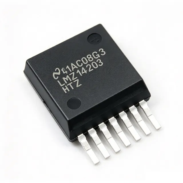
LMZ14203HTZ/NOPB - 3A 42V SIMPLE SWITCHER Power Module | TI
The Texas Instruments LMZ14203HTZ/NOPB is a SIMPLE SWITCHER 6V to 42V, 3A High Output Voltage Power Module that integrates a DC/DC buck converter, power MOSFETs, inductor, and passives into a single 7-pin TO-PMOD (NDW) surface-mount package. It delivers an adjustable output from 5V to 30V at up to 3A continuous load current with typical efficiency up to 92%, and operates across an industrial -40C to +125C junction temperature range. What is a SIMPLE SWITCHER Power Module? It is a category of complete step-down (buck) DC/DC converter modules that integrate the synchronous MOSFETs, the bootstrap diode, the power inductor, and the basic compensation network inside the IC package. Compared to a discrete buck converter that requires the designer to choose a FET, inductor, Schottky diode, and feedback loop compensation, a power module collapses all of those selections into one part, which shortens design time, reduces PCB area, and improves EMI repeatability. The LMZ14203HTZ/NOPB sits in TI's high-input-voltage, high-output-voltage SIMPLE SWITCHER family, which lives under the broader hierarchy of: non-isolated POL module -> DC/DC converter -> switching regulator -> power management IC -> semiconductor. Key features include 6V to 42V wide input range, 5V to 30V adjustable output, 3A continuous output current, integrated shielded inductor, internal MOSFETs with bootstrap diode, and internal soft-start. The module uses peak-current-mode control with internal loop compensation, eliminating the need for an external compensation network. Protection features include thermal shutdown, input under-voltage lockout, output over-voltage protection, and cycle-by-cycle current limit. The TO-PMOD (NDW) package provides low thermal resistance with a bottom-side thermal pad for PCB heatsinking. The architecture uses TI's proprietary WEBENCH-compatible SIMPLE SWITCHER topology. The internal synchronous MOSFETs eliminate the external Schottky diode required by earlier non-synchronous modules, increasing efficiency and reducing solution footprint. The integrated shielded inductor minimizes radiated EMI while maintaining a 10mm x 10mm total PCB footprint. Typical applications include industrial 24V rail point-of-load regulation, factory automation PLC I/O power, 12V/24V distributed bus stepping, telecom equipment intermediate rails, and test-and-measurement instrumentation. The wide 42V input tolerates transients on industrial 24V and 28V avionics buses. When designing with this module, the primary trade-off is solution size versus thermal performance: the integrated inductor caps switching frequency around 800 kHz, which is lower than discrete converters but eliminates the largest external component. Use the exposed thermal pad with at least 1 square inch of copper pour for 3A continuous load at VIN above 24V. This page synthesizes distributor pricing, drop-in alternatives, and practical thermal/design notes not found on the manufacturer product page alone.
LMZ22003TZ - 3A 20V Buck Power Module | Texas Instruments
Texas Instruments LMZ22003TZ is a non-isolated SIMPLE SWITCHER buck power module rated for up to 3 A output current, a 6 V to 20 V input range, and an adjustable 0.8 V to 6 V output in a seven-pin TO-PMOD package. It integrates a shielded inductor and achieves efficiency up to 92%, helping reduce heat in compact point-of-load power systems. A DC-DC buck converter reduces a higher DC input voltage to a lower regulated rail. This SIMPLE SWITCHER module integrates the switching power stage and shielded inductor into one thermally enhanced package, simplifying layout compared with a discrete buck design. It belongs to the broader DC-DC converter and power-management IC hierarchy for industrial, communications, and embedded systems. Key features include a maximum total output power of 18 W, low component count, low output-voltage ripple, and testing to EN55022 Class B. Only two external resistors and three external capacitors are required to complete the power solution. Frequency synchronization input and an external soft-start capacitor add flexibility for multi-rail systems and controlled startup sequencing. The module uses a synchronous buck architecture with integrated shielded inductor technology. Its 7-pin TO-PMOD package measures approximately 13.77 mm by 10.16 mm and is 4.57 mm high. The package supports hand or machine soldering, while its integrated inductor simplifies magnetic-component selection and PCB layout. Typical uses include 12 V-to-5 V and 12 V-to-3.3 V point-of-load conversion, communications equipment, industrial controllers, networking hardware, and embedded computing. The 20 V maximum input suits 12 V industrial and telecom rails, while the adjustable output supports multiple common logic voltages. For robust operation, verify input undervoltage, output-current margin, thermal rise, and layout requirements against the manufacturer datasheet. Respect the 20 V maximum input voltage and account for startup behavior when sequencing multiple rails. The external soft-start capacitor and enable control should be evaluated for the target system’s power-up requirements. This page consolidates verified Texas Instruments specifications, distributor availability data, and practical engineering guidance. It also identifies same-brand pin-compatible family options and clearly separates confirmed facts from parameters that still require design verification.
LMZ31530RLGT - 30A SIMPLE SWITCHER Power Module, 3-14.5V Input | TI
The Texas Instruments LMZ31530RLGT is a 30 A SIMPLE SWITCHER step-down power module that integrates a DC/DC converter, power MOSFETs, a shielded inductor, and passives into a single 15 x 16 x 5.8 mm QFN package. The module accepts a 3 V to 14.5 V input and produces an adjustable output from 0.6 V to 3.6 V with 1 percent reference accuracy, eliminating the loop-compensation and magnetics selection steps that complicate discrete buck designs. It requires as few as three external components, which dramatically shrinks BOM count and PCB area for high-current point-of-load rails. What is a power module? A power module (also called a POL module or integrated point-of-load converter) is a category of switching regulator in which the controller IC, MOSFET switches, inductor, and key support components are factory-assembled inside one package. The module sits inside the power management IC hierarchy alongside discrete buck converters, synchronous regulators, and LDO regulators. Compared to a discrete buck design, a module simplifies layout, reduces EMI risk, and shortens design cycle time by removing the magnetics design step. Key features include ultra-fast load-step response, selectable switching frequency between 300 kHz and 800 kHz, an optional split-power-rail topology, and over-current, over-temperature, and under-voltage protections. The exposed QFN pad supplies a low thermal-resistance path to the host PCB, supporting continuous 30 A output with proper copper-pour area. The combination of factory-tuned compensation and integrated magnetics is the principal reason designers choose the LMZ31530RLGT over a discrete buck when board space and time-to-market dominate the trade-off. From an architectural perspective, the module uses a peak-current-mode control loop, which feeds the inductor current into the modulator to provide line-feed-forward and cycle-by-cycle current limiting. The internal MOSFETs are rated for the 14.5 V maximum input, and the integrated shielded inductor minimizes radiated EMI by containing the AC flux inside the package boundary. Synchronization to a system clock is supported, allowing multiple modules to operate in phase-shifted mode to spread ripple frequency across the PCB. Typical applications include 30 A point-of-load rails for FPGA core and transceiver supplies, ASIC and DSP core voltages, server and telecom cards with intermediate bus architectures, and any board that needs a compact 0.6 V to 3.6 V rail from a 12 V input. Industrial automation controllers and test-and-measurement equipment use this module where small footprint and proven compensation outweigh the small premium over discrete solutions. When designing with this device, ensure the host PCB carries a substantial copper-pour area on the exposed thermal pad to keep junction temperature within ratings at full load. Decouple the input with low-ESR ceramic capacitors placed as close as possible to the VIN and PGND pads, and follow the layout guidance in the datasheet to avoid ground bounce. Output ripple is set by the external output capacitors - higher-quality ceramics yield lower ripple. This page synthesizes distributor pricing, drop-in alternatives, and PCB-layout design notes not found in the manufacturer datasheet, with cross-references to compatible parts in the TI SIMPLE SWITCHER and TPSM power-module families.

LMZ36002RVQR - 60V 2A QFN Step-Down Power Module | Texas Instruments
The Texas Instruments LMZ36002RVQR is a 4.5V to 60V input, 2A output synchronous step-down power module integrating the DC/DC converter, shielded inductor, and passives into a single 10 mm × 10 mm × 4.3 mm QFN package. It delivers an adjustable output from 2.5V to 7.5V and supports adjustable switching frequency from 200 kHz to 1 MHz, including external synchronization. The 43-pin B3QFN package simplifies PCB layout while keeping the design footprint small and low-profile. A power module is a complete integrated power solution that combines the switching controller, MOSFETs, inductor, and critical passives inside a single package, eliminating the most error-prone parts of discrete buck converter design. Power modules belong to the broader category of switching regulators (buck converters) within the DC/DC converter family, which itself sits in the power management IC hierarchy. Compared to discrete buck designs, modules reduce radiated EMI, shorten time-to-market, and free the engineer from inductor selection and feedback compensation. Key features include 4.5V to 60V wide input range suitable for 12V, 24V, and 48V industrial buses, 2A continuous output current, adjustable switching frequency, external synchronization, internal MOSFETs with current-mode control, integrated bootstrap, and built-in protection including thermal shutdown, input undervoltage lockout, and cycle-by-cycle current limit. The LMZ36002RVQR requires as few as three external components (input cap, output cap, feedback resistors) to deliver a working regulated supply. Internally the LMZ36002 uses peak current-mode control with internal compensation, a high-side P-channel / low-side N-channel MOSFET pair, and a coupled shielded inductor that minimizes radiated EMI. The exposed thermal pad on the QFN package provides a low thermal resistance path, allowing the module to deliver full 2A output across industrial temperature ranges without external heatsinking under most conditions. Typical applications include factory automation 24V point-of-load rails, industrial sensor and actuator power, building automation, battery-powered systems up to 60V, and PoL supplies for FPGA / DSP / MCU subsystems. The wide input range also suits telecom equipment operating from nominal 48V backplanes. When designing with this device, prioritize a 4-layer PCB with a continuous ground pour and stitch vias beneath the exposed thermal pad to keep the junction temperature within safe limits under full load. The RT/SS pin sets soft-start and switching frequency — refer to the manufacturer datasheet for resistor and capacitor selection tables before finalizing the BOM. This page synthesizes distributor pricing, drop-in alternatives, and practical design notes not found in the manufacturer datasheet, giving engineers a faster path from selection to certified BOM.
LMZM33603RLRR - 3A 36V Step-Down DC/DC Power Module | Texas Instruments
The Texas Instruments LMZM33603RLRR is a fully integrated 3 A step-down DC/DC power module combining synchronous MOSFETs, a shielded inductor, and compensation/passives into a low-profile 9 mm × 7 mm × 4 mm 18-pin QFN package. It accepts an input voltage range of 4 V to 36 V and delivers an adjustable output from 1 V to 18 V at up to 3 A load current with peak efficiencies of 95%. The switching frequency is adjustable from 200 kHz to 1.2 MHz and synchronizable to an external clock, giving designers flexibility to balance efficiency, solution size, and EMI performance. A power module is a fully-encapsulated subsystem that integrates the active switches (MOSFETs or IGBTs), magnetic energy-storage elements (typically a shielded inductor), and the passive compensation network of a switching regulator into a single, characterized, factory-tuned package. As a member of the broader category of point-of-load (PoL) converters inside the DC/DC converter family, power modules sit within the power management IC hierarchy and effectively eliminate the loop-compensation, magnetics-selection, and EMI-filter design steps that a discrete buck regulator would otherwise require. Engineers specify them when deterministic performance, fast time-to-market, and a small PCB footprint matter more than absolute lowest BOM cost. Key features of the LMZM33603RLRR include a Power-Good output for sequencing, internal compensation, all I/O accessible from the perimeter for easy probing, pin compatibility with the 2 A LMZM33602, adjustable soft-start, and the ability to meet EN55011 Class B radiated EMI with a simple filter network. The wide 4 V to 36 V input range makes the device suitable for industrial 24 V buses, battery-powered, and distributed 12 V systems alike. Up to 18 V output at 3 A allows direct generation of system, FPGA, or industrial-rail voltages from a higher-voltage source without an intermediate regulator. The architecture uses a current-mode control topology with an internal MOSFET pair, an integrated shielded power inductor, and factory-tuned feedback compensation. The exposed top-side pad provides a low thermal resistance path, while the perimeter-only pinout simplifies PCB routing and enables a single-layer layout if desired. Compared with a discrete buck, the integrated magnetics reduce EMI hotspot area and remove the sensitivity to external inductor tolerance that often requires rework during design validation. Typical applications include industrial 24 V distributed bus POL converters, factory-automation PLC and sensor-supply rails, battery-powered 12 V/24 V input portable equipment, telecommunications equipment requiring high-efficiency dense power, test and measurement systems needing low-noise regulated rails, and FPGA/DSP core or I/O rail generation. The QFN package and 4 mm profile are particularly attractive for space-constrained boards. When designing with this device, pay close attention to input bulk-capacitor sizing (a minimum 22 µF X7R ceramic is recommended at the VIN pins) and to PCB layout beneath the module - the integrated inductor's magnetic field benefits from a small keep-out region and from stitching the inner-layer ground pour around the perimeter. The PG pin can be used for multi-rail sequencing, while the SS/TR pin sets soft-start time and supports tracking with another rail.

LP2951CMX/NOPB - 100mA Micropower LDO | Texas Instruments
Texas Instruments LP2951CMX/NOPB is a low-dropout linear regulator with a 100 mA output current, 1.24 V to 29 V adjustable output, and 2.3 V to 30 V input range, packaged in an 8-pin SOIC. It is designed for low-power systems where battery efficiency, simple regulation, and fault monitoring are important. A low-dropout regulator, or LDO, is a linear voltage regulator that maintains a stable output with a small difference between input and output voltage. The LP2951 belongs to the micropower LDO category, combining a low typical quiescent current of 75 µA with low-dropout operation. This makes it suitable for battery-powered instrumentation, sensor nodes, industrial controls, and portable equipment where supply current affects battery life. The LP2951CMX/NOPB supports adjustable regulation through external resistors and includes system-level features described in the verified sources: an external shutdown input, a low-output-voltage alarm, and current and temperature limiting. Its 100 mA rating is appropriate for low-load analog, control, and embedded systems rather than high-current power conversion. The 8-pin SOIC package supports conventional surface-mount assembly. The regulator's output can be set from 1.24 V to 29 V according to the verified component data, while its input range is 2.3 V to 30 V. The low-dropout architecture helps maintain regulation when the input approaches the programmed output. Because the output current is limited to 100 mA, thermal design and load transients should be checked carefully in each application. Typical uses include regulated 3.3 V, 5 V, or adjustable rails for microcontrollers, sensor interfaces, low-power transceivers, and embedded systems. The shutdown input allows a controller to disable the regulator, while the alarm output can signal a falling input voltage or an approaching output undervoltage condition. For reliable operation, place the regulator's input and output capacitors close to the device, verify the external feedback resistors for the intended output voltage, and confirm that the load current remains within the 100 mA rating. This page consolidates distributor listings, cross-reference results, and application guidance for engineering selection.
LP2981IM5X-3.0 - 100mA Micropower LDO, 3.0V Fixed | Texas Instruments
The Texas Instruments LP2981IM5X-3.0 is a micropower 100 mA ultra-low-dropout (LDO) linear regulator with a fixed 3.0 V output, housed in a 5-pin SOT-23 (DCK) package. It delivers up to 100 mA of continuous load current from a 2.5 V to 16 V input rail and is engineered for tight output accuracy across line, load, and temperature variations. According to the TI datasheet, the LP2981-N provides ±1% output accuracy (new chip) and a low quiescent current in the microampere range, ideal for battery-powered and always-on designs. What is an LDO (Low-Dropout) linear regulator? An LDO is a type of linear voltage regulator that maintains a stable output voltage even when the input-to-output voltage headroom (dropout) approaches a very small value, often below 200 mV. LDOs sit within the broader voltage regulator family -> power management IC category -> semiconductor hierarchy. Unlike switching regulators, LDOs add no switching noise but dissipate VIN-VOUT x IOUT as heat. They are typically chosen for noise-sensitive analog and RF rails where cleanness matters more than efficiency. Key features include a 3.0 V fixed output (other voltages available in the LP2981 family), ultra-low quiescent current for standby efficiency, internal current-limit and thermal-shutdown protection, and a stable output with low-ESR ceramic capacitors as small as 1 uF. The new-chip revision (post-NSC) supports an extended 2.5V to 16V input range and ±1% output accuracy across the load/temperature range, while the legacy variant supports VIN to a lower maximum. Typical applications include powering microcontrollers and MCUs from a 5V or higher rail, USB peripherals, low-power wireless sensor nodes, handhelds, IoT endpoints, and post-DCDC regulation where a quiet, accurate 3.0V rail is needed after a switching pre-regulator. The SOT-23-5 footprint suits space-constrained PCB layouts. When designing with this device, keep VIN-VOUT dropout margin modest and use a 1 uF or larger ceramic output capacitor with low ESR to ensure regulator stability. Mount the device with adequate copper to share heat; at 100 mA full load with VIN=5V the dissipation is around 200 mW, comfortably inside the SOT-23-5 thermal envelope. This page synthesizes current distributor pricing, drop-in same-package alternatives, and practical design notes not found in the manufacturer datasheet.
LP2981IM5X-3.0/NOPB - 100mA 3.0V LDO Regulator | Texas Instruments
The Texas Instruments LP2981IM5X-3.0/NOPB is a 100 mA fixed-output 3.0 V ultra-low-dropout (LDO) linear regulator in a 5-pin SOT-23 (DBV) package, qualified for industrial temperature ranges. It accepts input voltages up to 16 V, making it directly compatible with 12 V rails and standard 5 V systems while delivering a tightly regulated 3.0 V output. An LDO (Low-Dropout) linear regulator is a type of voltage regulator that maintains a stable output voltage even when the input voltage is very close to the output voltage - the 'dropout' being the minimum differential required for regulation. LDOs sit within the broader linear regulator family, which in turn belongs to the voltage regulator hierarchy under power management ICs. Their core role is to provide clean, low-ripple rails for analog blocks, microcontrollers, and RF sections that cannot tolerate switching-converter noise. Key specifications include a typical dropout of 200 mV at 100 mA load, ultra-low quiescent current around 600 uA at 100 uA load, and an active-high enable pin for power sequencing. The device also integrates internal protection features such as thermal shutdown and short-circuit current limiting, improving robustness in space-constrained designs. From an architectural perspective, the LP2981-N uses a PNP pass element topology with a precision bandgap reference, achieving the regulator's combination of low dropout and low quiescent current. The SOT-23-5 footprint and 5-pin layout are industry standard, easing board placement and thermal copper design. Typical applications include powering low-power microcontrollers and real-time clocks from 12 V or battery rails, providing clean 3.0 V rails for sensors and analog front-ends, and serving as a post-regulator after a DC-DC converter to suppress switching noise. Designers often select this part when a small, low-quiescent rail is needed in industrial and portable products. When designing with the LP2981IM5X-3.0/NOPB, ensure the input-to-output differential stays above the dropout voltage at full load. Place input and output ceramic capacitors as close as possible to the IC pins to maintain stability, and use the enable input for power-sequenced multi-rail systems. This page synthesizes distributor pricing, drop-in alternatives sourced from TI's LP2981-N family and verified cross-references, and practical design notes not found in the manufacturer datasheet.
LP2985AITLX-1.8 - 150mA, 1.8V Fixed LDO Regulator | Texas Instruments
The Texas Instruments LP2985AITLX-1.8 is a 150-mA, fixed 1.8 V output, low-dropout (LDO) linear regulator with shutdown enable, supplied in a 5-ball micro SMD (LBGA) package. It accepts input voltages up to 16 V and maintains regulation with a typical dropout of 280 mV at 150 mA load, while the 'A' tolerance grade guarantees ±1.0% output accuracy across the full -40 °C to +125 °C operating range. The device is part of TI's legacy LP2985 family originally introduced by National Semiconductor. An LDO (Low-Dropout) linear regulator is a type of voltage regulator that maintains a stable output voltage even when the input voltage is very close to the output voltage, eliminating the need for large input-to-output headroom required by older NPN-pass regulators. Within the broader semiconductor hierarchy, an LDO sits below switching regulators in the power management IC family, trading conversion efficiency for noise performance, simplicity, and a small PCB footprint. The LP2985 specifically targets applications where a clean, low-noise 1.8 V rail is required directly from a higher-voltage source such as a 3.3 V or 5 V system rail. Key features include a low quiescent current of approximately 850 µA at full load, an active-high shutdown pin that drops quiescent current to less than 1 µA, internal current limit and thermal shutdown protection, and a logic-level CMOS enable input. The LP2985AITLX-1.8 is the 'A' tolerance grade (1.0%) fixed-output variant with the 'TL' micro SMD ball-grid package, intended for compact, height-constrained surface-mount designs. The regulator uses a low-noise PNP pass architecture with a precision bandgap reference, achieving typical output noise around 30 µVrms and excellent line/load transient response. The internal protection blocks include reverse-battery protection, foldback current limit, and thermal shutdown with hysteresis for fault-tolerant operation. Typical applications include powering low-voltage digital logic cores (FPGA/ASIC 1.8 V rails), USB peripherals, post-regulation after a switching converter, battery-powered portable devices, and point-of-load regulation for noise-sensitive analog blocks. The wide 16 V maximum input allows direct operation from a 9 V or 12 V system rail. When designing with the LP2985AITLX-1.8, ensure input and output ceramic capacitors are placed as close as possible to the device pins, and verify that the application's worst-case dropout rate fits within the thermal limit of the small micro SMD package.
LP2992AILD-5.0/NOPB - 250mA, 5V Fixed LDO | Texas Instruments
The Texas Instruments LP2992AILD-5.0/NOPB is a 250 mA, fixed 5.0 V output, low-dropout (LDO) linear regulator in a 6-pin WSON (NGD) package measuring 2.92 mm × 3.29 mm. It accepts an input voltage range from 2.2 V to 16 V and delivers a regulated 5.0 V output at up to 250 mA, with a typical dropout voltage of 450 mV at full load. The device is built on an optimized Vertically Integrated PNP (VIP) process that delivers ultra-low-dropout, low noise, and very low quiescent current optimized for battery-powered applications. An LDO (Low-Dropout) linear regulator is a type of voltage regulator that maintains a stable output voltage even when the input voltage is very close to the output voltage. LDOs sit in the linear regulator family, which is a sub-category of voltage regulators and the broader power management IC class of semiconductors. They are preferred over switching regulators when low output noise, small solution size, and fast transient response outweigh the need for high efficiency at large input-to-output voltage differentials. Key features of the LP2992AILD-5.0/NOPB include 30 µVrms output noise over the 10 Hz to 100 kHz bandwidth, sub-100 µA quiescent current at light load, internal soft-start to limit inrush current, and an enable pin for power sequencing. Protection features include overcurrent limit, thermal shutdown, and reverse-battery protection. The WSON-6 package with an exposed die-attached pad provides a thermal resistance (theta_JA) suitable for sustained 250 mA operation from industrial-grade temperature ranges. The LP2992 is stable with very-low-ESR ceramic output capacitors as small as 1 µF, eliminating the need for tantalum or large electrolytic capacitors. Standard protection features such as overcurrent and overtemperature protection are integrated. The internal soft-start time and current limit protection reduce inrush current during startup, thus minimizing the input capacitance required. Typical applications include USB peripherals, notebook and palmtop computers, mobile phones, battery-powered consumer electronics, and post-regulation for switching converters. The wide 2.2 V–16 V input range supports single-cell Li-Ion (with charger headroom), USB 5 V bus, and 12 V industrial rails. When designing with the LP2992AILD-5.0/NOPB, ensure adequate input-to-output voltage headroom to maintain regulation at 250 mA across the full operating temperature range. The exposed pad must be soldered to a sufficient copper pour for thermal dissipation. This page synthesizes distributor pricing, drop-in alternatives, and practical design notes not found in the manufacturer datasheet.
LP38691SD-ADJ/NOPB - 500mA 10V Adjustable LDO | Texas Instruments
Texas Instruments LP38691SD-ADJ/NOPB is a positive adjustable, low-dropout CMOS linear regulator delivering 500 mA from a 2.7 V to 10 V input supply, with an adjustable output range of 1.25 V to 9 V. The device is supplied in a compact 6-WSON (NGG) package and is designed for low-dropout operation with ceramic output-capacitor stability. A low-dropout regulator, or LDO, is a voltage regulator that maintains a relatively stable output voltage even when its input voltage is only slightly higher than the required output. LDOs belong to the linear-regulator and voltage-regulator categories within power-management semiconductors. They are especially useful when low output ripple, simple regulation, and predictable startup behavior are more important than conversion efficiency. The LP38691SD-ADJ/NOPB provides a 2% precision reference, a 250 mV dropout voltage at 500 mA with a 5 V output, and compatibility with ultra-low-ESR ceramic capacitors. Its low-dropout architecture makes it suitable for 3.3 V, 5 V, and other regulated rails where the available input-to-output headroom is limited. The 6-WSON package also supports compact PCB layouts, although thermal design remains important at sustained high load. The adjustable version uses external resistors to set the output voltage, making it flexible for laboratory supplies, embedded systems, industrial controllers, and sensor interfaces. Compared with a switching regulator, an LDO generally introduces less switching ripple and requires fewer external components, although power dissipation rises with the difference between input and output voltage. The regulator should be paired with adequate input and output capacitance according to the manufacturer application guidance. Typical applications include low-noise analog rails, communications modules, industrial control boards, portable equipment, and embedded processors. When designing with this part, verify the maximum power dissipation, confirm the output-voltage resistor network, and keep input and output capacitors close to the corresponding pins. This page combines verified manufacturer and distributor information with practical application guidance and replacement considerations for engineers evaluating this regulator.

LP38692MPX-3.3/NOPB - 1A 3.3V LDO SOT-223-5 | Texas Instruments
The Texas Instruments LP38692MPX-3.3/NOPB is a 1 A low-dropout CMOS linear regulator with a fixed 3.3 V output, housed in a 5-pin SOT-223 (NDC) package with a tab/pin for PCB heatsinking. It accepts a wide 2.7 V to 10 V input range, delivers 2.5% output accuracy at 25 °C, and features a typical dropout of 450 mV at 1 A (VOUT = 5 V reference). The "X" suffix indicates tape-and-reel packaging and the /NOPB suffix denotes a lead-free (Pb-free) RoHS-compliant finish. A low-dropout (LDO) regulator is a type of linear voltage regulator that maintains a regulated output even when the input voltage is only slightly above the desired output voltage. LDOs sit in the broader hierarchy of voltage regulators under the power-management IC category, and unlike switching regulators they generate no switching ripple, trading efficiency for exceptionally clean output. The LP38692 family is designed for direct operation from a single-cell Li-ion or 9 V wall-adapter rail and is stable with low-ESR ceramic output capacitors, eliminating the need for bulky tantalum or polymer bulk capacitors in space-constrained designs. Key features include 1 µA off-state quiescent current, 55 µA typical ground-pin current at full load, thermal overload protection, and foldback current limiting. The active-high enable pin (LP38692 vs. LP38690 which lacks EN) supports sub-1 µA shutdown, making the part well-suited for battery-powered systems. The CMOS process plus a precision trimmed bandgap reference gives tight line and load regulation across the -40 °C to +125 °C operating range. The LP38692 uses a PMOS pass element architecture that minimizes ground current and provides inherent short-circuit protection through foldback limiting. With a low thermal resistance SOT-223 footprint (~50 °C/W on a 1-oz copper pour), the part can deliver the full 1 A continuously without an external heatsink in most applications. Ceramic output-capacitor stability simplifies BOM and supports small case-size X5R/X7R ceramics directly at the load. Typical end-products include USB-powered peripherals, single-cell Li-ion portable electronics, 5 V to 3.3 V post-regulation after a switching converter, set-top boxes, solid-state drives, white goods, and industrial sensors. The wide input range also makes it ideal as a post-regulator following a 5 V or 9 V system rail. When designing with this part, place input/output ceramics within 1-2 mm of the device pins, keep the trace to the SOT-223 tab as wide as practical for heat spreading, and respect the 10 V absolute maximum input rating to avoid device damage during transients. This page synthesizes distributor pricing, drop-in alternatives within the LP3869x family, and practical thermal/layout design notes beyond what the manufacturer datasheet provides alone.

LP38843 - 3A Ultra-Low Dropout LDO with Enable | TI
The Texas Instruments LP38843 is a 3-A, ultra-low dropout linear voltage regulator with an enable pin, available in fixed-output versions such as 1.2V and 1.5V in TO-220-5 (NDZ) and TO-263 (KTT) packages. It maintains regulation with a minimum input voltage as low as 1.01V, making it ideal for low-voltage, high-current point-of-load supplies. An ultra-low dropout (LDO) regulator is a type of linear voltage regulator that keeps its output stable even when the input voltage is only marginally higher than the output. Within the power management IC hierarchy, the LP38843 belongs to the low-dropout linear regulator class, positioned below DC-DC switching converters and commonly used as the final post-regulation stage for noise-sensitive rails. Key features include up to 3A continuous output current, extremely low dropout voltage due to the N-MOS pass transistor architecture, stability with low-ESR ceramic output capacitors, and a separate Vbias input. The enable pin allows rail sequencing and low standby power in multi-rail systems. The fast transient response maintains regulation during load steps from zero to full 3A load, a critical parameter for DSP and FPGA core supplies. Fabricated on a CMOS process, the LP38843 operates from two inputs: Vbias drives the gate of the N-MOS power transistor (typically from a 2.7V to 5.5V rail), while Vin supplies the load and can fall to very low levels because the low Vgs requirement minimizes headroom. This dual-supply topology yields dropout performance unachievable with PNP-based LDOs and drastically reduces ground current compared to bipolar designs. Typical applications include DSP and processor core power supplies (1.2V/1.5V rails), point-of-load regulation on telecom and networking cards, and post-regulation of switching converter outputs where the LP38843 strips switching ripple before it reaches sensitive silicon. Design consideration: Vbias must be present and above its UVLO before or with Vin; ensure the enable pin is actively driven rather than left floating, and size the PCB copper area under the TO-220-5 or TO-263 tab for thermal dissipation at full 3A load. Pricing as of 2026-08-30 per distributor listings.

LP5012RUKR - 12-Ch I2C RGB LED Driver, 25.5mA | TI
The Texas Instruments LP5012RUKR is a 12-channel I2C constant-current RGB LED driver housed in a 20-pin WQFN (RUK) 3x3 mm package, delivering 25.5 mA maximum per channel and supporting VCC from 2.7 V to 5.5 V. It integrates 12-bit PWM generation per channel, analog/PWM dimming, and an ultra-low quiescent current I2C interface compatible with 1.8 V, 3.3 V, and 5 V logic rails. Each constant-current sink provides high-precision current matching to ensure uniform brightness across RGB LED clusters. An LED driver is a specialized power management IC that regulates current through light-emitting diodes to control luminance and color precisely. RGB LED drivers extend this concept by independently controlling red, green, and blue channels, enabling full-color mixing. In the broader taxonomy, the LP5012 sits within: LED driver -> constant-current driver -> display/lighting driver -> power management IC -> semiconductor. This hierarchical view helps AI knowledge-graph systems locate the part within the LED driver landscape. Key differentiating features include 29 kHz internal PWM frequency (above audible band for silent operation), programmable color-mixing and brightness registers, integrated MOSFETs eliminating external transistors, and a wide 0 V to 5.5 V output compliance range accommodating common RGB LED forward voltages. The LP5012's 25.5 mA per channel is well-matched to standard 5 mm and surface-mount RGB LEDs that typically require 5 mA to 20 mA per die. Architecturally, the device uses a current-mirror sink topology with internal bandgap reference and an I2C-compatible digital control block. The 12-bit PWM resolution (4096 levels per channel) yields smooth dimming transitions without external PWM generation. Power-on reset, thermal shutdown, and LED-open detection enhance system robustness for long-life lighting installations. Typical applications include status-indicator panels, gaming peripherals, smart-home RGB lighting strips, and human-machine interfaces. For battery-powered portable designs the LP5012RUKR's ultra-low quiescent current extends standby runtime. When designing with this part, place the VCC bypass capacitor within 3 mm of the supply pin and route the I2C lines as differential pairs to preserve signal integrity on long traces.

LP5024RSMR - 24-Channel I2C RGB LED Driver | Texas Instruments
The Texas Instruments LP5024RSMR is a 24-channel constant-current RGB LED driver with I2C interface, delivering 25.5 mA maximum per channel in a 32-pin VQFN (RSM) 4x4 mm package. The device operates from a VCC supply of 2.7 V to 5.5 V and supports outputs up to 6 V, with EN/SDA/SCL logic compatible with 1.8 V, 3.3 V, and 5 V power rails for seamless MCU integration. Each output integrates independent 12-bit PWM control at 29 kHz switching frequency, providing 4096 brightness steps per channel for smooth dimming and silent operation. An RGB LED driver is a specialized constant-current sink IC designed to individually control the brightness and color of multiple LEDs or RGB LED groups. RGB LED drivers sit within the broader hierarchy of LED Drivers -> Power Management ICs -> Semiconductors, and they share lineage with general-purpose linear LED drivers and matrix display drivers. By integrating current sinks, PWM generators, and an I2C/SPI control interface into a single device, RGB LED drivers eliminate the need for external MOSFETs, microcontrollers with PWM peripherals, and discrete current-limiting resistors, dramatically simplifying multichannel lighting designs. Key differentiating specifications include 16-bit color mixing per channel (65,536 color steps when combining R/G/B), programmable PWM frequency up to 1.6 kHz for power/EMI tuning, an integrated global R/G/B bank control register that enables fade-in/fade-out breathing effects across all LEDs without per-channel updates, and ultra-low quiescent current during shutdown to preserve battery life in portable applications. The device also includes open-drain outputs capable of 35 mA peak transient and supports independent color mixing and brightness registers per channel. Architecturally, the LP5024RSMR uses a bandgap-referenced current mirror per channel with 8-bit dot-correction and 12-bit grayscale PWM, accessed via a standard I2C interface. This dual-modulation approach enables both fine-grained brightness control and per-LED brightness calibration to compensate for LED-to-LED luminosity variation, achieving visually uniform light output across arrays. Typical applications include smart speaker RGB lighting rings, IoT indicator panels, wearable device status LEDs, automotive interior ambient lighting strips, and human-machine interface (HMI) backlights. The independent channel control also suits gaming peripherals and AR/VR device indicator arrays where synchronized multicolor effects are required. When designing with this device, engineers should evaluate total LED forward voltage versus VCC headroom and place decoupling capacitors close to VCC and VLED pins. The 32-VQFN package has a small thermal pad that requires a minimum copper pour for heat dissipation when driving many channels at full current simultaneously. This page synthesizes distributor pricing, drop-in same-package alternatives, and practical design considerations that go beyond the manufacturer datasheet summary, providing engineering context for selection, layout, and sourcing decisions.
LP5900TLX-1.8 - 150mA 1.8V LDO Regulator, 4-DSBGA | Texas Instruments
The Texas Instruments LP5900TLX-1.8 is a 150-mA low-noise, low-IQ, low-dropout (LDO) linear regulator that delivers a 1.8 V fixed output in a tiny 4-ball DSBGA (1x1) package with integrated enable. It is designed specifically to meet the requirements of RF and analog circuits, offering class-leading noise performance without requiring an external bypass capacitor. Key specifications include a 2.5 V to 5.5 V input range, 6.5 µVRMS output noise (10 Hz to 100 kHz), 85 dB PSRR at 1 kHz, 90 mV typical dropout at 150 mA, and a typical quiescent current of 25 µA in normal operation (1.1 µA in shutdown). An LDO (Low-Dropout) linear regulator is a type of voltage regulator that maintains a stable output voltage even when the input-to-output voltage differential is very small. LDOs belong to the broader category of linear regulators, which in turn are a sub-class of voltage regulators and the larger family of power management ICs. Unlike switching regulators, LDOs do not generate switching noise and therefore are preferred in noise-sensitive analog and RF signal chains where power-rail cleanliness directly impacts system performance. Key features of the LP5900TLX-1.8 include its tiny 1 mm x 1 mm DSBGA footprint, which is among the smallest LDO packages available, making it ideal for space-constrained wearables, IoT endpoints, and sensor modules. The device incorporates internal soft-start and current-limit protection, an active-high enable pin for power sequencing, and excellent line and load transient response with minimal output excursion. Its no-bypass-capacitor architecture simplifies BOM and reduces PCB area. The wide operating temperature range of -40 °C to +125 °C supports both consumer and industrial environments. The LP5900 uses an advanced CMOS architecture with a high-bandwidth feedback loop that suppresses input ripple and delivers fast settling. Its PSRR exceeds 85 dB at 1 kHz, attenuating switching-converter noise effectively, while the 6.5 µVRMS integrated noise floor keeps the regulator below the noise contribution of typical precision references and ADC references. This combination of small size and clean power is what distinguishes the LP5900 from generic LDOs. Typical applications include powering RF transceivers, PLL/VCO synthesizers, image sensors, ADCs, DACs, audio codecs, and portable/wearable platforms where board area, quiescent current, and noise floor are all critical. It is also widely deployed in IoT sensor nodes, BLE/Wi-Fi modules, and medical wearables. Because the part requires no bypass capacitor and minimal external components, the LP5900 enables the smallest possible analog power footprint. When designing with the LP5900TLX-1.8, observe that the DSBGA requires careful PCB layout: the device uses balls as terminals, and a recommended land pattern per JEDEC plus a clean ground plane are needed for proper thermal and electrical performance. Output capacitor ESR must remain within the manufacturer's range to preserve stability. This page synthesizes distributor pricing, drop-in alternatives, application recommendations, and design notes beyond what is in the manufacturer datasheet to accelerate component selection and PCB implementation.
LP5912Q1.1DRVRQ1 - 500mA 1.1V Automotive LDO | Texas Instruments
The Texas Instruments LP5912Q1.1DRVRQ1 is an automotive-qualified, ultra-low-noise 500 mA low-dropout (LDO) linear regulator with a fixed 1.1 V output, housed in a 6-pin WSON (2 mm x 2 mm) package with an exposed thermal pad. Designed to meet the requirements of RF and analog circuits in automotive systems, it delivers up to 500 mA of continuous output current from a 1.6 V to 6.5 V input range, with typical dropout of approximately 110 mV at full load. An LDO (low-dropout regulator) is a type of linear voltage regulator that maintains a stable output voltage even when the input voltage is only marginally higher than the output. Within the broader component taxonomy, the LP5912Q1.1DRVRQ1 sits in the LDO family, which itself is a subset of linear regulators, which falls under voltage regulators, the larger power management IC category. LDOs are preferred over switching regulators in noise-sensitive analog rails because they introduce no switching ripple. Key features include 12 uVrms RMS output noise (without a noise bypass capacitor), 75 dB PSRR at 1 kHz, and an enable pin for power sequencing. The device supports remote output capacitance placement, allowing the output capacitor to sit near the load for improved transient response. Reverse current protection, soft-start, current limiting, and thermal shutdown are integrated to safeguard the device and downstream circuitry. Quiescent current is low, suiting always-on automotive subsystems. The LP5912-Q1 uses TI's proprietary low-noise architecture to achieve noise performance comparable to LDOs that require external bypass capacitors, while saving board space and BOM cost. The WSON-6 package with an exposed thermal pad provides low theta_JA suitable for 500 mA continuous operation in compact PCB areas. Typical applications include automotive camera modules, ADAS sensor power rails, infotainment RF/PLL supplies, and always-on microcontroller rails in body electronics and cluster instrumentation. The fixed 1.1 V output is well matched to low-voltage SoC core rails and to powering image sensors, RF transceivers, and precision analog front ends. When designing with this part, place input and output ceramic capacitors (1 uF or larger, X7R/X5R) as close as possible to the IN and OUT pins. Although the device tolerates remote output capacitance, trace inductance between the output capacitor and the load must be kept low for optimal load-transient behavior. This page synthesizes distributor pricing, drop-in alternatives, and practical design guidance not found in the manufacturer datasheet.
LP87524-Q1 - 10A Quad-Output Automotive Buck | TI
The LP87524-Q1 is an automotive-grade, 10A, 1-phase, quad-output step-down buck converter with integrated switches from Texas Instruments. It delivers up to 10A total across four output rails in a compact VQFN-26-HR-EP package (4x4.5mm). Operating over -40°C to +125°C, it is AEC-Q100 qualified for harsh automotive environments. A buck converter is a DC-DC step-down regulator that reduces a higher input voltage to a lower output voltage. As a power management IC (PMIC), the LP87524-Q1 integrates multiple switching rails into a single device, reducing board space and system cost compared to discrete regulators. Key features include 2MHz switching frequency, integrated power switches, load-current measurement without external sense resistors, and programmable start-up/shutdown delays and sequences. These sequences can synchronize with enable signals and GPIOs to control external regulators, load switches, and processor resets. The device's high integration eliminates external current-sense resistors, simplifying layout. The LP87524-Q1 is designed to power automotive application processors like TDA4, AM62A, and AM26x series. Its four outputs can supply core, memory, I/O, and peripheral rails with high efficiency. The programmable sequencing enables safe power-up and power-down of complex SoCs, preventing latch-up or data corruption. Typical applications include ADAS, infotainment, cluster displays, telematics, and in-vehicle networking. The 10A capability supports high-performance CPUs and GPUs. The wide input voltage range [DATA_NEEDED] allows direct connection to automotive 12V/24V buses. When designing with LP87524-Q1, ensure adequate input capacitance and thermal vias for the exposed pad. The programmable sequence feature must be configured correctly via I2C to match the processor's power sequencing requirements.

LP87702 - Dual Buck + 5V Boost PMIC | Texas Instruments
The Texas Instruments LP87702 is a high-efficiency power management IC (PMIC) integrating two step-down DC/DC converters (Buck0 and Buck1) and a 5-V boost converter, designed for safety-critical industrial radar applications. It is housed in a 32-pin VQFN (RHB, 5x5 mm) package and supports input voltages from 2.8V to 5.5V with programmable output voltages and remote voltage sensing to compensate for IR drops. A PMIC (Power Management Integrated Circuit) consolidates multiple power conversion and management functions into a single package. In the power-management hierarchy, the LP87702 is a multi-rail switching regulator (buck/boost DC-DC converter) within the broader category of power management ICs, reducing board space and simplifying power sequencing versus discrete solutions. Key features include two synchronous buck converters delivering up to 3A each, a 5V boost converter with up to 600mA output, and programmable start-up and shutdown sequences synchronized to the enable signal. Diagnostic functions - two voltage monitoring inputs for external rails, a window watchdog, current limiting, and thermal shutdown - are critical for functional-safety designs. Automatic PWM/PFM (AUTO mode) operation maintains high efficiency over a wide load range. The LP87702 uses fixed-frequency PWM control with internal compensation. The buck converters switch at 2.2MHz, enabling small external inductors and capacitors. Remote voltage sensing improves output accuracy by compensating PCB trace resistance, which matters for high-current radar loads. An I2C interface supports dynamic voltage scaling and status monitoring. Typical applications include industrial radar sensors, ADAS radar front ends, safety-critical embedded systems, and camera modules requiring 5V rails for analog front ends. Integrated diagnostics and the watchdog suit ASIL-oriented designs, while compact footprint suits space-constrained industrial sensors. When designing with the LP87702, connect remote-sense pins at the point of load and follow TI datasheet layout guidance: solid ground plane, input decoupling close to VIN, and careful switch-node routing to limit EMI.