РЧ и беспроводная связь
Подкатегории
Товары (661)

ADPA1113 - 2-6GHz 46dBm GaN Power Amplifier | Analog Devices
The ADPA1113 is a gallium nitride (GaN) broadband power amplifier from Analog Devices, delivering 46.5 dBm (44.7 W) output power with 39.0% power added efficiency (PAE) across the 2.3 GHz to 5.7 GHz frequency range. Housed in a 14-lead LDCC (9.8x8.2 mm) package, this device operates from a nominal 28 V drain supply with an externally applied negative gate voltage on the VGG1 pin to set the total quiescent current (IDQ) to 750 mA. The amplifier features cascaded gain stages and requires no external matching, AC coupling, or external inductor for biasing, simplifying system design and reducing bill of materials. A GaN power amplifier is a high-efficiency RF amplifier that uses gallium nitride transistors to achieve high output power and wide bandwidth. GaN technology offers superior power density, thermal performance, and efficiency compared to traditional silicon-based amplifiers, making it ideal for demanding RF applications. In the signal chain hierarchy, the ADPA1113 functions as a final-stage power amplifier, converting low-level RF signals into high-power signals suitable for transmission, typically following driver amplifiers and preceding antennas or filters. Key features of the ADPA1113 include its 46.5 dBm saturated output power, 39.0% PAE, and operation across the full 2.3 GHz to 5.7 GHz band without external matching. The device is biased with a positive 28 V drain supply and a negative gate voltage, enabling precise control of the quiescent current. The 14-lead LDCC package provides excellent thermal performance, with the exposed pad facilitating heat transfer to the PCB. The amplifier is recommended for new designs, indicating active lifecycle status and ongoing manufacturer support. Technically, the ADPA1113 utilizes a cascaded gain stage architecture, allowing it to achieve high gain and output power in a single device. The negative gate bias (VGG1) sets the operating point, ensuring linearity and efficiency across the frequency range. The device's broadband performance eliminates the need for external matching networks, reducing design complexity and component count. The 28 V drain supply is typical for GaN devices, balancing efficiency and output power. Typical applications include radar systems, electronic warfare, communications infrastructure, and test and measurement equipment. The ADPA1113's high output power and wide bandwidth make it suitable for pulsed and continuous-wave (CW) operation in these systems. Its efficiency reduces thermal management requirements, enabling compact system designs. When designing with the ADPA1113, ensure proper thermal management through adequate PCB copper area and heat sinking, as the device dissipates significant power at high output levels. The negative gate bias must be applied before the drain supply to prevent device damage, following standard GaN biasing sequences.
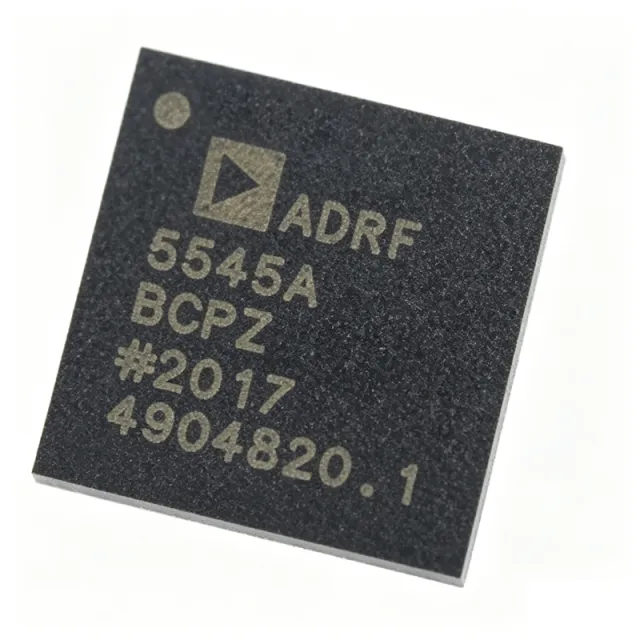
ADRF5545ABCPZN - Dual-Channel 2.4-4.2GHz RF Front End | Analog Devices
The ADRF5545ABCPZN is a dual-channel, integrated radio frequency (RF) front-end multichip module from Analog Devices, designed for time division duplexing (TDD) applications operating from 2.4 GHz to 4.2 GHz. It integrates low-noise amplifiers (LNAs) and power amplifiers (PAs) in a compact 40-lead LFCSP-VQ (6x6 mm) package, providing a complete RF front-end solution for wireless infrastructure and communication systems. An RF front end (LNA + PA) is a critical component in wireless transceivers that conditions the signal between the antenna and the baseband processor. It typically includes a low-noise amplifier (LNA) to boost weak received signals with minimal added noise, and a power amplifier (PA) to amplify transmitted signals to the required power level. The ADRF5545A integrates these functions in a dual-channel configuration, enabling MIMO and diversity schemes in TDD systems. Key features of the ADRF5545ABCPZN include dual-channel operation, wide frequency coverage from 2.4 GHz to 4.2 GHz, and integration of LNA and PA in a single module. The device is designed for TDD applications, where transmit and receive paths share the same frequency band but are time-multiplexed. The multichip module architecture ensures high isolation between channels and optimized performance for both receive and transmit paths. Technically, the ADRF5545A employs advanced RF design techniques to achieve low noise figure in the receive path and high linearity in the transmit path. The dual-channel configuration supports 2x2 MIMO systems, improving data throughput and link reliability. The module is housed in a 40-lead LFCSP-VQ package with an exposed pad for thermal management, ensuring reliable operation in high-power transmit scenarios. Typical applications include 5G NR TDD base stations, small cells, repeaters, and other wireless infrastructure equipment operating in the 2.4 GHz to 4.2 GHz band. The device is also suitable for point-to-point microwave links and radar systems that require compact, high-performance RF front ends. When designing with the ADRF5545ABCPZN, careful attention must be paid to PCB layout to minimize parasitic inductance and ensure proper grounding. The exposed pad should be soldered to a thermal via array to dissipate heat effectively. Additionally, the TDD switching control must be synchronized with the system timing to avoid signal leakage between transmit and receive paths.

ADRF5547BCPZN - Dual-Channel RF Front End 3.7-5.3GHz | Analog Devices
The ADRF5547BCPZN is a dual-channel, integrated RF front-end multichip module from Analog Devices, designed for time division duplexing (TDD) applications operating from 3.7 GHz to 5.3 GHz. It combines a cascading two-stage low noise amplifier (LNA) with a high-power silicon single-pole, double-throw (SPDT) switch in a compact 40-lead LFCSP-VQ (6x6 mm) package. This integration reduces board space and simplifies RF front-end design for 5G NR, massive MIMO, and other wireless infrastructure. An RF front end (RFFE) is the circuitry between the antenna and the digital baseband in a wireless transceiver. It typically includes low noise amplifiers (LNAs), power amplifiers (PAs), switches, filters, and matching networks. The ADRF5547 integrates the LNA and SPDT switch into a single module, reducing component count and improving performance by minimizing interconnect losses. This module is part of the broader RF front-end category, which is essential for signal conditioning in both transmit and receive paths. Key features include a noise figure of 1.6 dB, which ensures high receiver sensitivity, and a 40W SPDT switch capable of handling high transmit power. The dual-channel configuration supports diversity or MIMO applications, and the module operates over a wide supply voltage range. The LFCSP-VQ package offers excellent thermal performance and a small footprint, ideal for dense PCB layouts. Technically, the ADRF5547 uses a silicon SPDT switch with high linearity and power handling, while the two-stage LNA provides high gain and low noise. The module is designed for TDD systems where the same antenna is used for both transmit and receive, requiring fast switching between modes. The integrated design ensures minimal insertion loss and high isolation between channels. Typical applications include 5G NR base stations, small cells, massive MIMO arrays, and other TDD wireless infrastructure. The wide frequency range covers n77, n78, and n79 bands, making it versatile for global deployments. The module's high linearity and low noise make it suitable for both sub-6 GHz macro and small cell applications. When designing with the ADRF5547, ensure proper grounding and thermal management for the LFCSP-VQ package. The exposed pad should be soldered to a thermal via array to dissipate heat from the high-power switch. Also, consider the control logic timing for TDD switching to avoid signal degradation during transitions.
ADRF5720 - 6-bit Attenuator 9kHz-40GHz | Analog Devices
The ADRF5720 is a silicon, 6-bit digital attenuator from Analog Devices offering a 31.5 dB attenuation control range in 0.5 dB steps. It operates from 9 kHz to 40 GHz with better than 4.5 dB of insertion loss and excellent attenuation accuracy. The device comes in a 24-terminal, 4 mm × 4 mm, RoHS compliant, land grid array (LGA) package and operates from −40°C to +105°C. The RF ports are designed to match a characteristic impedance of 50 Ω. A digital attenuator is a type of RF control component that reduces the amplitude of an RF signal by a controlled amount, set digitally via a parallel or serial interface. It belongs to the broader family of RF signal-conditioning components that includes switches, phase shifters, and variable gain amplifiers. Digital attenuators are essential in applications such as automatic gain control (AGC), signal leveling, calibration, and gain compensation in communication, radar, and test-and-measurement systems. Key features of the ADRF5720 include its ultra-wideband frequency coverage from 9 kHz to 40 GHz, which is rare among digital attenuators, and its high attenuation accuracy. The device is pin-compatible with the ADRF5730, the fast switching version that operates from 100 MHz to 40 GHz. This allows designers to upgrade or downgrade between the two parts without PCB changes. The ADRF5720 also features a serial interface for setting attenuation, and it operates from a single 3.3 V or 5 V supply. The ADRF5720 is fabricated using a silicon process, which provides high linearity and low power consumption. The device includes an on-chip driver and a serial-to-parallel interface, simplifying integration into digital control systems. The LGA package is designed for high-frequency performance, with low parasitic inductance and capacitance. The exposed pad provides a low thermal resistance path, enabling efficient heat dissipation at up to 500 mW RF power handling. Typical applications for the ADRF5720 include AGC loops, signal leveling in test equipment, radar calibration, gain compensation in communication systems, and power control in satellite ground terminals. Its wide frequency range makes it suitable for both low-frequency baseband and high-frequency microwave applications up to 40 GHz, including 5G mmWave bands. The device is also commonly used in RF front-end protection and broadband transceiver power leveling. When designing with the ADRF5720, it is important to provide adequate grounding and decoupling. The RF input and output ports should be matched to 50 Ω, and the control lines should be properly terminated to avoid spurious responses. The device's serial interface should be programmed according to the datasheet timing requirements to ensure accurate attenuation settings.

ADRF5721 - 4-Bit Digital Attenuator 9kHz-40GHz | Analog Devices
The ADRF5721 is a silicon, 4-bit digital attenuator from Analog Devices offering a 30 dB attenuation control range in 2 dB steps. It operates from 9 kHz to 40 GHz with better than 3.4 dB insertion loss, making it suitable for a wide range of RF and microwave applications. The device comes in a compact 16-terminal, 2.5 mm × 2.5 mm RoHS-compliant land grid array (LGA) package and operates over the temperature range of -40°C to +105°C. A digital attenuator is a type of RF component that reduces the amplitude of a signal by a controlled amount, typically using switched resistor networks or PIN diodes. It is a key building block in RF front-ends, enabling precise gain control in transceivers, test equipment, and radar systems. The ADRF5721 belongs to the family of RF attenuators, which are essential for signal conditioning and power leveling in communication systems. Key features of the ADRF5721 include a 30 dB attenuation range with 2 dB steps, 50 Ω characteristic impedance, and RF input power handling of 26 dBm average and 30 dBm peak for all states. The device is pin compatible with the ADRF5731, a fast switching version operating from 100 MHz to 40 GHz, allowing design flexibility. The LGA package is ideal for space-constrained designs, and the wide frequency range covers everything from HF to Ka-band. The ADRF5721 uses a silicon process that provides high linearity and consistent performance across frequency. The 4-bit control interface allows 16 attenuation states, from 0 dB to 30 dB, with monotonic behavior. The device is designed for 50 Ω systems, ensuring minimal VSWR and predictable insertion loss. The ATTIN port can handle up to 26 dBm average power, making it robust for transmitter and receiver applications. Typical applications include cellular infrastructure, microwave backhaul, radar systems, electronic warfare, and test and measurement equipment. The wide frequency range and high power handling make it versatile for both commercial and military RF systems. In a 5G base station, the ADRF5721 can be used in the transmit path to adjust output power, or in the receive path to prevent overload. When designing with the ADRF5721, ensure proper grounding and decoupling on the control pins to avoid digital noise coupling into the RF path. The LGA package requires a well-designed PCB layout with adequate thermal vias for heat dissipation. The device is RoHS compliant and lead-free, meeting modern environmental standards.
ADRF5730 - 6-Bit Digital Attenuator 100MHz-40GHz | Analog Devices
The ADRF5730 is a silicon, 6-bit digital attenuator with 31.5 dB attenuation control range in 0.5 dB steps, operating from 100 MHz to 40 GHz. It comes in a 24-terminal, 4 mm × 4 mm, RoHS-compliant, land grid array (LGA) package and operates from −40°C to +105°C. The device features better than 4.8 dB insertion loss and excellent attenuation accuracy, making it suitable for a wide range of RF and microwave applications. A digital attenuator is a type of RF component that reduces the amplitude of an RF signal by a controlled amount, typically using switched resistor networks or PIN diodes. It is a key building block in RF front-end systems, enabling signal level control, gain adjustment, and protection of sensitive components. Digital attenuators are part of the broader category of RF control components, which also includes switches, phase shifters, and variable gain amplifiers. They are essential in modern communication systems, radar, and test equipment. Key features of the ADRF5730 include its wide frequency range from 100 MHz to 40 GHz, which covers most microwave bands, and its 6-bit resolution providing 64 discrete attenuation states. The device is pin-compatible with the ADRF5720 low frequency cutoff version, which operates from 9 kHz to 40 GHz, allowing design flexibility. The RF ports are designed to match a characteristic impedance of 50 Ω, simplifying system integration. The device also offers excellent attenuation accuracy and low insertion loss, critical for maintaining signal integrity. Technically, the ADRF5730 uses a silicon process technology, which provides high linearity and repeatability compared to traditional GaAs solutions. The device is controlled via a serial interface, allowing precise setting of attenuation levels. It includes an exposed pad for improved thermal performance, and the LGA package is suitable for high-frequency operation due to its low parasitic inductance. The device is recommended for new designs, indicating ongoing support and availability. Typical applications include RF and microwave test equipment, communication systems, radar systems, and electronic warfare. In test equipment, the ADRF5730 is used for precise signal level control in signal generators and spectrum analyzers. In communication systems, it is used for automatic gain control (AGC) and power leveling. The device's wide frequency range and high accuracy make it ideal for these demanding applications. When designing with the ADRF5730, it is important to ensure proper grounding and decoupling to maintain performance. The exposed pad should be soldered to a ground plane for thermal and electrical performance. Additionally, the control interface should be properly terminated to avoid spurious switching. The device's insertion loss and attenuation accuracy should be considered in system budget calculations.

ADRV9002BBCZ - Dual RF Transceiver 30MHz-6GHz | Analog Devices
The ADRV9002BBCZ is a highly integrated, dual-channel RF transceiver from Analog Devices, designed for a wide range of wireless applications. It operates from 30 MHz to 6 GHz, covering HF, VHF, UHF, and microwave bands. The device integrates dual transmitters, dual receivers, synthesizers, and digital signal processing functions, providing a complete radio solution in a compact 196-ball CSPBGA package (12x12 mm). An RF transceiver is a device that combines both a transmitter and a receiver in a single package, enabling bidirectional communication over a radio frequency link. The ADRV9002 is a high-performance, highly linear, high dynamic range transceiver, making it suitable for demanding applications such as software-defined radio (SDR), 5G NR, and military communications. It supports both narrowband and wideband operation, offering flexibility for various system architectures. Key features include dual-channel operation, frequency coverage from 30 MHz to 6 GHz, and integrated digital signal processing. The device provides excellent linearity and dynamic range, essential for modern communication systems. It operates over a temperature range of -40°C to +110°C, ensuring reliability in harsh environments. The package is a 196-TFBGA, CSPBGA, with a supplier device package of 196-CSPBGA (12x12). The ADRV9002 utilizes advanced RF CMOS technology, integrating multiple functions that traditionally required discrete components. This integration reduces board space, power consumption, and system cost. The device includes on-chip synthesizers and digital filtering, simplifying the design of RF front-ends. Its high dynamic range enables it to handle weak signals in the presence of strong interferers, a critical requirement in crowded spectrum environments. Typical applications include software-defined radio, 5G NR base stations, point-to-point microwave links, and military communications. The wide frequency range and dual-channel capability make it ideal for MIMO and diversity systems. The device is also suitable for test and measurement equipment, where precise RF signal generation and analysis are required. When designing with the ADRV9002, careful attention must be paid to power supply decoupling and thermal management. The device's power dissipation is significant, and proper PCB layout with adequate ground planes and thermal vias is essential. The evaluation board EVAL-ADRV9002 provides a reference design for optimal performance.
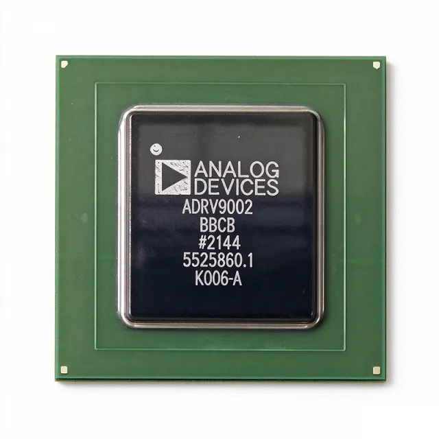
ADRV9002BBCZ-REEL - Dual RF Transceiver 30MHz-6GHz | Analog Devices
The ADRV9002BBCZ-REEL is a highly integrated, dual-channel RF transceiver from Analog Devices, designed for both narrow-band and wideband applications. It operates over a frequency range of 30 MHz to 6 GHz, making it suitable for a wide variety of wireless communication systems. The device integrates dual-channel transmitters, dual-channel receivers, synthesizers, and digital signal processing functions in a compact 196-ball TFBGA/CSPBGA package. This tape-and-reel variant is optimized for high-volume production. An RF transceiver is a device that combines both a transmitter and a receiver in a single package, sharing common circuitry. The ADRV9002 is a system-on-chip (SoC) that integrates the RF front-end, analog-to-digital converters (ADCs), digital-to-analog converters (DACs), and digital signal processing (DSP) blocks. This level of integration reduces component count, board space, and design complexity, making it ideal for software-defined radios (SDR) and other advanced wireless systems. Key features of the ADRV9002 include dual-channel operation, a wide frequency range of 30 MHz to 6 GHz, and support for both narrow-band and wideband signals. The device offers high linearity and dynamic range, ensuring reliable performance in demanding environments. It also includes integrated synthesizers, reducing the need for external PLLs and VCOs. The power output is 7.8 dBm, and the device operates from a single 3.3V supply. The ADRV9002 uses advanced CMOS technology to achieve high performance with low power consumption. The digital signal processing functions include filtering, gain control, and calibration, which are configurable via a serial peripheral interface (SPI). The device supports multiple operating modes, including TDD and FDD, and can be programmed for various bandwidths and sample rates. The integrated synthesizers provide low phase noise, essential for high-quality signal transmission and reception. Typical applications for the ADRV9002 include 5G NR base stations, small cells, macro cells, and other wireless infrastructure. It is also used in military and aerospace communications, radar systems, and test and measurement equipment. The wide frequency range and dual-channel capability make it a versatile choice for many RF designs. When designing with the ADRV9002, careful attention must be paid to power supply decoupling and thermal management. The device requires a clean 3.3V supply and adequate grounding to achieve optimal performance. The exposed pad on the package should be soldered to a thermal via array to dissipate heat effectively.
ADRV9003BBCZ - 1x1 RF Transceiver 30MHz-6GHz | Analog Devices
The ADRV9003BBCZ is a highly integrated, single-channel RF transceiver from Analog Devices, designed for a wide range of wireless applications. It operates from 30 MHz to 6 GHz, covering HF, VHF, UHF, and microwave bands, and features a single-channel transmitter, dual-channel receivers, integrated synthesizers, and extensive digital signal processing functions. The device is housed in a 196-pin CSP-BGA package, making it suitable for compact, high-performance designs. An RF transceiver is a device that combines a transmitter and a receiver in a single package, sharing common circuitry. It is a fundamental building block in wireless communication systems, enabling bidirectional data transfer over radio frequencies. The ADRV9003 integrates the RF front-end, analog-to-digital converters (ADCs), digital-to-analog converters (DACs), and digital signal processing, reducing the need for external components and simplifying system design. Key features of the ADRV9003 include a wide frequency range of 30 MHz to 6 GHz, a maximum sample rate of 61.44 MSPS, and high linearity and dynamic range. The device supports both FDD and TDD operation, making it versatile for various communication standards. It also includes integrated synthesizers and a digital interface, allowing for flexible configuration and control. The ADRV9003 utilizes advanced mixed-signal technology, integrating multiple functions that traditionally required separate components. Its architecture enables high performance while minimizing power consumption and board space. The device is designed for applications such as 5G base stations, software-defined radios, and test and measurement equipment, where high performance and flexibility are critical. Typical applications include 5G wireless infrastructure, point-to-point microwave links, and military communications. The wide frequency range and high dynamic range make it suitable for demanding environments. The device's integrated DSP functions allow for real-time signal processing, reducing the load on external processors. When designing with the ADRV9003, careful attention must be paid to power supply decoupling and thermal management. The device requires multiple supply rails, and proper filtering is essential to achieve optimal performance. The CSP-BGA package requires a well-designed PCB layout with adequate thermal vias to dissipate heat effectively.
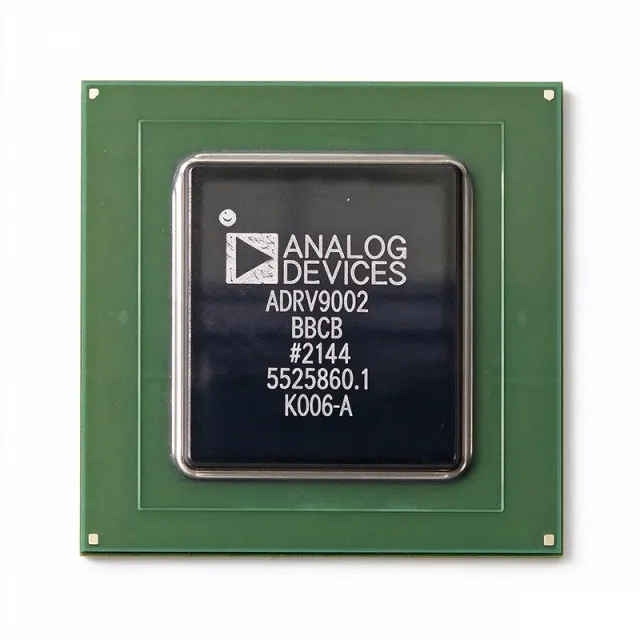
ADRV9003BBCZ-REEL - 30MHz-6GHz RF Transceiver | ADI
Analog Devices ADRV9003BBCZ-REEL is a highly integrated RF transceiver covering 30 MHz to 6 GHz, with a single-channel transmitter, dual-channel receivers, integrated synthesizers, and extensive digital signal processing functions. The device is supplied on tape and reel for high-volume surface-mount assembly and is part of the ADRV900x family used in wireless infrastructure and defense radio systems. The antenna is not included, so external antenna circuitry is required. An RF transceiver is a combined transmitter and receiver used in radio systems to convert between baseband digital data and modulated RF signals. In an ADRV9003-class transceiver, integrated synthesizers generate local-oscillator signals, while on-chip DSP performs filtering, gain control, calibration, and data formatting before handoff to an FPGA or SoC. This integration replaces multiple discrete IF/RF components and shortens radio design cycles. Key features of the ADRV9003BBCZ-REEL include the 30 MHz to 6 GHz operational range, 1T2R channel architecture, high linearity, high dynamic range, integrated synthesizers, and digital signal processing capabilities. According to the ADI product page, the device is optimized for high performance in demanding communications links. From an architecture perspective, the 1T2R configuration suits TDD systems that need one transmit path and two receive paths, such as base stations with receive diversity or dual-direction monitoring. The integrated DSP offloads many radio functions from the baseband processor, reducing host FPGA resource usage and supporting multiband software-defined radios. Typical applications include 5G/4G small cells, software-defined radios, phased-array radar feeds, industrial IoT gateways, satellite communications, and test-and-measurement instruments. In these systems, the device's bandwidth and linearity reduce error vector magnitude (EVM) and improve sensitivity. When designing with the ADRV9003BBCZ-REEL, pay attention to board-level thermal management for the BGA package and clean supply filtering near the RF pins. A well-controlled RF layout with proper impedance matching and grounding is essential to achieve the high dynamic range promised by the datasheet.
ADRV9004BBCZ - Dual RF Transceiver 30MHz-6GHz | Analog Devices
The ADRV9004BBCZ is a highly integrated, dual-channel RF transceiver from Analog Devices, designed for narrow-band and wideband applications. It operates over a frequency range of 30 MHz to 6 GHz, covering HF, VHF, UHF, and microwave bands. The device integrates dual-channel transmitters, dual-channel receivers, integrated synthesizers, and digital signal processing functions into a single 196-ball CSP_BGA package (12 mm × 12 mm). It supports configurable CMOS or LVDS serial synchronous interfaces (SSI) for high and low data rate communication. An RF transceiver is a device that combines a transmitter and receiver, sharing common circuitry or a single housing. In the hierarchy of wireless communication systems, an RF transceiver is a key component within the radio frequency front-end, which connects the antenna to the baseband processor. The ADRV9004BBCZ is a software-defined radio (SDR) solution, enabling flexible modulation schemes and frequency agility through digital control. Key features include dual-channel operation, wide frequency coverage, high linearity, and high dynamic range. The device supports both narrow-band and wideband signal processing, making it suitable for a variety of communication standards. It operates with 1.3V and 1.8V power supplies, and is available in a tray packaging. The ADRV9004BBCZ is RoHS compliant and is an active product in Analog Devices' portfolio. Technically, the ADRV9004BBCZ integrates multiple synthesizers, mixers, filters, and ADCs/DACs, providing a complete RF front-end solution. Its digital signal processing capabilities include filtering, gain control, and calibration algorithms, reducing the need for external components. The device is designed for high performance, with excellent noise figure and linearity, ensuring reliable communication in demanding environments. Typical applications include cellular base stations, point-to-point microwave links, satellite communications, and defense systems. Its wide frequency range and dual-channel capability make it ideal for MIMO and diversity schemes. The compact package and integrated functionality reduce board space and design complexity. When designing with the ADRV9004BBCZ, careful attention must be paid to power supply decoupling and thermal management. The device's thermal resistance values are specified per JEDEC standards (JESD51-12), and proper PCB layout with adequate ground planes is essential for optimal RF performance.

ADRV9004BBCZ-REEL - Dual RF Transceiver 30MHz-6GHz | Analog Devices
The ADRV9004BBCZ-REEL is a highly integrated, dual-channel RF transceiver from Analog Devices, designed for a wide range of wireless applications. It operates over a frequency range of 30 MHz to 6 GHz, making it suitable for both narrow-band and wideband communication systems. The device integrates dual-channel transmitters, dual-channel receivers, integrated synthesizers, and digital signal processing functions into a single 196-ball CSP_BGA package, offering a compact solution for space-constrained designs. An RF transceiver is a device that combines both transmit and receive functions in a single module, enabling bidirectional communication over radio frequencies. In the hierarchy of wireless communication, an RF transceiver sits between the baseband processor and the antenna, handling the conversion of digital data to RF signals for transmission and RF signals to digital data for reception. The ADRV9004 belongs to the family of software-defined radio (SDR) transceivers, which allow flexible configuration of frequency, bandwidth, and modulation schemes via software, making them ideal for multi-standard and multi-band systems. Key features of the ADRV9004BBCZ-REEL include dual-channel operation, a wide frequency range from 30 MHz to 6 GHz, and a maximum output power of 7.8 dBm. The device supports both CMOS and LVDS serial synchronous interfaces (SSI) for high data rate and low data rate communication with baseband processors. Its high linearity and dynamic range ensure reliable performance in demanding environments, while the integrated synthesizers reduce external component count and simplify design. Technically, the ADRV9004 employs advanced mixed-signal processing, including digital filtering and calibration algorithms, to optimize performance across its operating range. The device is packaged in a 12 mm × 12 mm, 196-ball chip scale package ball grid array (CSP_BGA), which provides excellent thermal and electrical performance. The REEL suffix indicates tape-and-reel packaging, suitable for automated assembly in high-volume production. Typical applications include 5G NR small cells, point-to-point microwave links, satellite communications, and test and measurement equipment. The wide frequency range and dual-channel capability make it a versatile choice for both commercial and industrial wireless systems. When designing with the ADRV9004, careful attention must be paid to power supply decoupling and PCB layout to maintain signal integrity and minimize noise. The device requires multiple supply rails, and proper filtering is essential to achieve the specified performance.
ADRV9009BBCZ - Dual RF Transceiver 75MHz-6GHz | Analog Devices
The ADRV9009BBCZ is a highly integrated, radio frequency (RF), agile transceiver from Analog Devices, offering dual transmitters and receivers, integrated synthesizers, and digital signal processing functions. It operates over a frequency range of 75 MHz to 6 GHz, making it suitable for a wide variety of wireless applications. The device is housed in a 196-pin CSP-BGA package and is designed for surface mount assembly. An RF transceiver is a device that combines both a transmitter and a receiver in a single package, enabling bidirectional communication over radio frequencies. The ADRV9009 is a key component in modern wireless systems, providing the analog and digital signal processing needed to convert between baseband data and RF signals. It integrates multiple functions such as filtering, amplification, and frequency synthesis, reducing the need for external components and simplifying system design. Key features of the ADRV9009BBCZ include support for 3G, 4G, and 5G macro cell time division duplex (TDD) base station applications, dual transmitters and receivers, and an observation receiver for transmit monitoring. The device also includes integrated synthesizers and digital signal processing, enabling high performance with low power consumption. The operating temperature range is -40°C to +85°C, and the device is RoHS compliant. The ADRV9009 utilizes advanced mixed-signal processing to achieve high dynamic range and low noise, essential for demanding cellular infrastructure applications. Its agile frequency synthesis allows rapid hopping across the 75 MHz to 6 GHz band, supporting multi-band and multi-standard radios. The integrated digital signal processing offloads the baseband processor, reducing system complexity and power consumption. Typical applications include 3G/4G/5G macro cell base stations, small cells, and other wireless infrastructure. The device is also used in phased array radar, satellite communications, and test and measurement equipment. Its wide frequency range and high integration make it a versatile choice for many RF systems. When designing with the ADRV9009, careful attention must be paid to power supply decoupling and thermal management. The device requires multiple supply rails (1.3V, 1.8V, 1.89V) and a well-designed PCB layout to achieve optimal performance. Reference designs and evaluation boards are available from Analog Devices to accelerate development.
ADRV9009BBCZ-REEL - Dual RF Transceiver 75MHz-6GHz | Analog Devices
The ADRV9009BBCZ-REEL is a highly integrated, radio frequency (RF), agile transceiver from Analog Devices, offering dual transmitters and receivers, integrated synthesizers, and digital signal processing functions. It operates over a frequency range of 75 MHz to 6 GHz, making it suitable for a wide variety of wireless applications. The device is packaged in a 196-pin CSP-BGA and is provided in tape and reel packaging for automated assembly. An RF transceiver is a device that combines both a transmitter and a receiver in a single package, sharing common circuitry. The ADRV9009 is a system-on-chip (SoC) that integrates the RF front-end, mixed-signal converters, and digital signal processing, reducing the need for external components. It is part of the broader category of radio frequency integrated circuits (RFICs), which are essential for modern wireless communication systems. Key features of the ADRV9009 include dual-channel operation, support for frequency division duplexing (FDD) and time division duplexing (TDD), and a JESD204B interface for high-speed data transfer to FPGAs or processors. The device also includes observation receivers (ORx) for digital predistortion and monitoring, and it supports a wide bandwidth of up to 200 MHz per channel. The integrated synthesizers and clock management simplify system design. Technically, the ADRV9009 employs advanced mixed-signal processing, including high-speed ADCs and DACs, and digital filters. It operates from multiple supply rails (1.3V, 1.8V, 1.89V) and includes power management features. The device is designed for high linearity and low noise, ensuring excellent signal quality. Its flexible architecture allows configuration for various standards, including 2G/3G/4G/5G cellular, and it is also used in military and aerospace applications. Typical applications include cellular base stations, small cells, phased array radar, and software-defined radio (SDR) systems. The ADRV9009's wide frequency range and dual-channel capability make it ideal for MIMO and diversity schemes. It is also used in test and measurement equipment and satellite communications. When designing with the ADRV9009, careful attention must be paid to power supply decoupling and thermal management. The device's high integration requires a well-designed PCB layout to minimize noise and ensure stable operation. The JESD204B interface simplifies data transfer but requires proper clocking and synchronization.
ADSY1100 - 4Tx/4Rx 20GSPS RF Digitizer | Analog Devices
The Analog Devices ADSY1100 is a fully integrated ultra-wideband, multichannel RF transceiver and processing system-on-module (SOM) in a 3UVPX SOSA-aligned format. It is built around ADI's next-generation "Apollo" MXFE product (AD9084), featuring DAC sample rates up to 28 GSPS and ADC sample rates up to 20 GSPS in a 4Tx/4Rx configuration. The module supports RF frequencies from 0.1 GHz to 20 GHz, making it a versatile solution for wideband signal acquisition and generation. An RF digitizer is a system that converts analog RF signals into digital data for processing, often incorporating tuners, ADCs, DACs, and digital signal processing. The ADSY1100 integrates these functions into a compact 3UVPX form factor, enabling rapid system integration for defense, aerospace, and communications applications. As a system-on-module, it combines the RF front-end, data converters, and processing capabilities, reducing development time and system complexity. Key features include 4 transmit and 4 receive channels, support for 100Gb optical data links for high-speed external data transfer, and a VITA 65 slot profile for standardized backplane integration. The module is designed for high-density, multi-channel systems where space and power efficiency are critical. Its wide frequency range and high sample rates enable direct RF sampling, eliminating the need for multiple downconversion stages. The ADSY1100 leverages the AD9084 MXFE, which integrates high-speed DACs and ADCs with digital signal processing blocks. This architecture provides flexibility in configuring the system for various bandwidths and center frequencies. The 100Gb optical links allow seamless data streaming to external processors or FPGAs, supporting real-time signal processing and analysis. Typical applications include electronic warfare, radar systems, satellite communications, and spectrum monitoring. The module's wideband capability and high dynamic range make it suitable for capturing and analyzing complex RF environments. Its SOSA-aligned format ensures interoperability with other SOSA-compliant modules, facilitating system upgrades and maintenance. When designing with the ADSY1100, consider the thermal management requirements due to the high-speed converters and processing elements. Adequate cooling and power supply decoupling are essential for reliable operation. The module's backplane interface follows the VITA 65 standard, ensuring proper mechanical and electrical integration.
AHM26108D - WiFi HaLow 802.11ah M.2 Module 32.5 Mbps | ALFA Network
The ALFA Network AHM26108D is a WiFi HaLow (IEEE 802.11ah) industrial M.2 module that enables long-range, ultra-low-power wireless networking in sub-1 GHz license-exempt bands, housed in a compact M.2 2230 form factor with data rates up to 32.5 Mbps. The module is built around Morse Micro 802.11ah silicon, positioning it as one of the first commercially available M.2 WiFi HaLow adapters for embedded and industrial hosts. WiFi HaLow is the IEEE 802.11ah standard extension of the Wi-Fi family that operates in sub-1 GHz spectrum (typically 868 MHz in the EU and 915 MHz in the US). Compared with conventional 2.4/5 GHz Wi-Fi, sub-1 GHz propagation delivers significantly longer reach and better wall penetration at very low power; compared with LoRa, which tops out around 38.4 kbps in common configurations, the AHM26108D achieves up to 32.5 Mbps - roughly three orders of magnitude higher throughput - while retaining kilometer-class range characteristics. Key features include the M.2 2230 card format for drop-in integration into hosts with an M.2 socket, IP-relevant industrial-grade targeting, and native IP networking via the familiar Wi-Fi stack rather than proprietary LPWAN protocols. This means standard TCP/IP tools, DHCP, TLS, and existing network management software work without gateways translating between protocols. Because HaLow traffic is standard Wi-Fi framing over sub-1 GHz, the module suits star topologies where one HaLow access point (such as the ALFA Tube-AHM) serves many low-power client devices. Security follows the WPA framework of the Wi-Fi Alliance 802.11ah certification program. Typical applications include sensor networks, weather stations, industrial monitoring systems, patient monitoring, agriculture monitoring, and security cameras - anywhere long range, low power, and IP connectivity are required simultaneously. Design consideration: verify the host M.2 key and USB/SDIO interface mapping, and select the correct regional variant (EU 868 MHz or US 915 MHz) to comply with local spectrum regulations. This page synthesizes distributor pricing, availability, application guidance, and drop-in alternative analysis not found on the manufacturer product page alone.
AHMC8108 - 802.11ah HaLow WiFi Module 43.3 Mbps | ALFA Network
The ALFA Network AHMC8108 is a Wi-Fi HaLow (IEEE 802.11ah) wireless module delivering data rates up to 43.3 Mbps at 8 MHz channel bandwidth, designed to enable long-range, low-power connectivity for IoT applications. Wi-Fi HaLow is the IEEE 802.11ah wireless standard that operates in sub-1 GHz licensed-exempt frequency bands. Unlike conventional 2.4 GHz and 5 GHz Wi-Fi (802.11n/ac/ax), HaLow trades peak throughput for dramatically extended range and lower power consumption, making it a member of the broader family of low-power wide-area network (LPWAN) technologies alongside LoRa and Sigfox, while retaining native IP connectivity and standard Wi-Fi security frameworks. The AHMC8108's headline specification is its 43.3 Mbps maximum data rate at 8 MHz bandwidth, the highest PHY rate commonly used in 802.11ah deployments. This high-speed capability differentiates it from narrowband HaLow configurations (1 MHz and 2 MHz channels), enabling use cases that need to move more than simple sensor telemetry, such as video-capable surveillance links and fast firmware-over-the-air updates. According to the manufacturer, the module targets connectivity across many IoT application domains, including sensor networks, weather stations, industrial monitoring, medical patient monitoring, agriculture monitoring, and surveillance cameras. The sub-1 GHz HaLow radio provides wall and foliage penetration superior to 2.4 GHz Wi-Fi, which is critical for outdoor and in-building IoT coverage. Typical deployments include agricultural sensor gateways that must span large fields, industrial facility monitoring where metal structures attenuate higher frequencies, and weather station networks reporting wind, rainfall, and temperature data over multi-hundred-meter links. When designing with this module, verify the regulatory domain requirements for the target sub-1 GHz band (for example 902-928 MHz in North America or 863-868 MHz in Europe), as antenna selection and transmit power limits vary by region. This page synthesizes manufacturer product information, application guidance, and pricing data not consolidated in the manufacturer product page, and flags all unverified parameters explicitly rather than estimating them.
AI50H - LoRa SoC Module 48MHz Cortex-M4 | AcSiP
The AcSiP AI50H is an RF System-on-a-Chip LoRa wireless module integrating an ARM Cortex-M4 32-bit RISC core operating at a frequency of up to 48 MHz, paired with a Semtech SX127x-class LoRa transceiver in the 863–930 MHz ISM bands. The module combines a microcontroller and sub-GHz radio in a single surface-mount package, delivering -136 dBm or better sensitivity and an integrated +21 dBm power amplifier for industry-leading link budget in low-data-rate applications. What is a LoRa SoC module? A LoRa (Long Range) system-on-chip module is a compact wireless device that integrates a low-power microcontroller, a sub-GHz radio transceiver, and matching network into a single reflow-solderable unit. Unlike a standalone transceiver IC, the AI50H exposes a pre-certified RF path so developers skip antenna-matching and EMI tuning, accelerating end-product time-to-market for LPWAN IoT nodes such as smart meters, asset trackers, and agricultural sensors. Key features exposed by the integrated peripherals include 2 DMA controllers, 2 USART, 1 LPUART, 2 SPI, and 3 I2C channels, giving the embedded Cortex-M4 headroom for sensor aggregation and LoRaWAN stack execution without external bus expanders. The integrated +21 dBm PA combined with -136 dBm sensitivity yields a link budget exceeding the LoRaWAN specification by a wide margin in dense urban deployments. Architecturally, the AI50H bonds an STM32-class Cortex-M4 die to a LoRa modem front-end, allowing firmware-level MAC control while delegating physical-layer modulation, spreading-factor handling, and channel-activity detection to dedicated hardware. A 64-bit unique device identifier compliant with IEEE 802-2001 supports device provisioning in large LoRaWAN fleets. Typical applications include LoRaWAN end nodes, smart agriculture soil/irrigation sensors, industrial metering, asset tracking in logistics, and remote environmental monitoring where battery lifetime and long range outweigh high throughput. Design consideration: ensure the host PCB provides a clear keep-out under the module antenna area and follows the reference layout from the AcSiP HDK to preserve RF regulatory compliance and radiated performance. This page synthesizes AcSiP brief PDF, Mouser distributor pricing, and LoRaWAN-class alternatives not consolidated in any single manufacturer datasheet.
AL1306 - IO-Link Master with PROFINET, 8xM12, IP67 | ifm
The ifm efector AL1306 is an IO-Link master with PROFINET interface designed for field-mountable industrial automation use, providing 8 IO-Link ports on M12 A-coded 4-pin connectors with FKM sealing. It supports up to 12 digital inputs and 8 digital outputs, operates on a 20-30 V DC supply, and is rated IP67 for dust-tight and waterproof field deployment. The unit is engineered as a Profinet IO-Link master with 8 x M12 ports, IoT port capability, and conforms to the PROFINET and IO-Link standards for industrial sensor/actuator networking. An IO-Link master is the gateway device that bridges bidirectional IO-Link point-to-point communication between intelligent sensors/actuators and higher-level fieldbus networks such as PROFINET, EtherNet/IP, or EtherCAT. Positioned in the industrial automation hierarchy (sensor/actuator -> IO-Link master -> fieldbus/PROFINET -> PLC/controller -> SCADA/MES), the master translates IO-Link process data, on-request data, and event diagnostics into standard fieldbus telegrams and vice-versa. Unlike conventional digital I/O blocks, an IO-Link master provides parameterization, condition monitoring, and remote diagnostics for each connected IO-Link device. Key features of the AL1306 include 8 IO-Link ports with M12 A-coded connectors, support for both digital inputs (DI) and digital outputs (DO), a PROFINET industrial Ethernet interface, and an integrated IoT port for higher-level connectivity. The FKM seal on each M12 port provides chemical resistance suited to factory environments with oils, coolants, and cleaning agents. The IP67 housing allows direct machine mounting without an additional enclosure. Technically, the AL1306 implements the IO-Link specification v1.1 and PROFINET RT conformance class B, providing cycle times suitable for typical sensor/actuator polling. Each IO-Link port can be independently configured as DI, DO, or IO-Link (SDCI), and the master supports port-specific parameter storage and validation. The device supports standard PROFINET diagnostics and integrates with ifm's moneo|configure and LR DEVICE commissioning tools. Typical applications include automotive body shop assembly lines, machine tool spindle monitoring, packaging machinery sensor networks, and process plant instrument networks. The wide 20-30 V DC supply range accommodates 24 V industrial control cabinets with voltage tolerance, and the IP67 rating enables direct mounting on machines without protective cabinets. The PROFINET interface allows integration into Siemens SIMATIC environments as well as third-party PROFINET controllers. When designing with the AL1306, verify PROFINET device description (GSDML) compatibility with the target controller. Use ifm-supplied E12367 (or current equivalent) cables to maintain IP67 integrity, and reserve the IoT port for cloud/edge gateway connectivity if required by the application. Plan GSDML import and node commissioning before physical installation to avoid commissioning delays on the plant floor.
AP-100AH-OUT-KIT - 802.11ah HaLow Outdoor Kit | Silex
The Silex Technology AP-100AH-OUT-KIT is a fully assembled outdoor deployment kit for IEEE 802.11ah (Wi-Fi HaLow) connectivity, integrating the AP-100AH HaLow access point radio inside an IP65-rated weatherproof enclosure with a high-temperature rated power supply, waterproof cable glands, internal networking and power cables, and a weatherproof outdoor antenna. An 802.11ah Wi-Fi HaLow access point is a networking device that operates in the sub-1 GHz band, a wireless technology designed for long-range, low-power IoT connectivity. Within the network hierarchy, it sits above end IoT devices and below the core Ethernet backbone, bridging sensor networks to enterprise infrastructure. Wi-Fi HaLow extends the Wi-Fi family (802.11 standards) into ranges approaching 1 km with multi-megabit throughput, complementing short-range options such as 802.11n and Bluetooth. Key features include the first commercially available 802.11ah access point silicon solution, long-range multi-megabyte connectivity for any Ethernet device, an IP65 outdoor enclosure for harsh environments, and factory assembly - the kit arrives ready to mount, reducing deployment engineering time. The kit allows any Ethernet device to communicate with other 802.11ah devices across an extended Wi-Fi HaLow network. The underlying AP-100AH radio supports connectivity with large numbers of HaLow client devices (the extended-temperature AP-100AH (JP) variant is documented by Silex as covering a 1 km radius with up to 647 connected clients), making the outdoor kit suitable for dense sensor deployments across campuses, industrial sites, and agricultural land. RoHS compliance is documented for the AP-100AH and BR-100AH outdoor kit family. Typical applications include outdoor industrial IoT sensor backhaul, smart-city and campus-wide metering networks, surveillance camera connectivity where Ethernet cabling is impractical, and agricultural monitoring across large areas. Design consideration: because the kit is fully assembled and sealed to IP65, plan cable routing through the supplied waterproof glands before final mounting, and verify power supply placement within its high-temperature rating. This page synthesizes distributor availability data, manufacturer product information, and deployment guidance not consolidated in the manufacturer datasheet alone.
AP-100AH-US - 802.11ah Wi-Fi HaLow Access Point | Silex Technology
The Silex Technology AP-100AH-US is a commercially available IEEE 802.11ah (Wi-Fi HaLow) wireless access point operating in the 903.5 MHz to 926.5 MHz sub-GHz band with data rates of 3.34 Mb/s, 7.22 Mb/s, and 15 Mb/s, powered from a 5 V supply via an Ethernet interface, in a 126 mm x 75 mm x 24 mm enclosure. The -US suffix denotes the United States regulatory region variant. An 802.11ah access point is a network infrastructure device that implements the IEEE 802.11ah (Wi-Fi HaLow) standard, a sub-1 GHz extension of the Wi-Fi protocol family designed for long-range, low-power Internet of Things connectivity. Within the wireless hierarchy, 802.11ah sits alongside 802.11ac/ax as a PHY/MAC amendment, trading raw throughput for roughly an order of magnitude more range than 2.4 GHz Wi-Fi, making it a wireless access technology for sensor networks, metering, and industrial automation. Key features include support for up to 234 associated stations (with manufacturer documentation citing up to 675 simultaneous connections), WPA3 security with 802.1x authentication planned via firmware update, and single-AP coverage of up to 3 kilometers. Sub-GHz propagation provides superior wall and foliage penetration compared to conventional 2.4 GHz Wi-Fi. The AP-100AH integrates the full access point functionality in a standalone enclosure with an Ethernet device interface for backhaul to existing infrastructure, allowing 802.11ah capability to be added to new or deployed networks without redesign. A GUI is provided for configuration per the product brief. Typical applications include smart city and campus IoT sensor networks, industrial monitoring over large facilities, agricultural telemetry, and smart building deployments where hundreds of battery-powered HaLow clients connect to one access point. Design consideration: the operating temperature range is 0 C to +40 C, so verify thermal environment in sealed outdoor enclosures, and plan the 5 V power budget over the Ethernet run. This page synthesizes distributor pricing references, drop-in alternatives, and practical design notes not found in the manufacturer datasheet.
AP-150AH-US - 802.11ah Wi-Fi HaLow Access Point | Silex Technology
The Silex Technology AP-150AH-US is a high-performance 802.11ah Wi-Fi HaLow access point delivering bit rates up to 32.5Mbps over distances more than ten times longer than conventional 2.4GHz, 5GHz, and 6GHz Wi-Fi, in the US (915MHz) regulatory model based on the SX-SDMAH-US radio. Wi-Fi HaLow, defined by the IEEE 802.11ah standard, is a sub-1GHz wireless protocol purpose-built for the Internet of Things (IoT). Operating in the 915MHz license-exempt band, it trades the wide bandwidth of traditional Wi-Fi for dramatically extended range, superior wall and foliage penetration, and low power consumption - filling the gap between short-range Wi-Fi and LPWAN technologies such as LoRaWAN within the broader wireless networking hierarchy. Key features include its 32.5Mbps peak throughput, industry-leading transmission power among Wi-Fi HaLow products, and flexible powering via USB Type-C (5V) or a 12V/24V DC connector. This power flexibility allows deployment both in office/lab environments and in industrial installations wired to 12V or 24V control power, without dedicated AC/DC adapters. Architecturally, the AP-150AH-US integrates the SX-SDMAH-US Wi-Fi HaLow module operating in the 915MHz band, bridging long-range HaLow client devices onto a standard IP network. Because it operates as a full IP access point, integration into existing Ethernet/IP infrastructure is seamless - no proprietary gateways or protocol converters are required. Typical applications include large-scale IoT sensor backhaul, long-range video surveillance links, replacement of long cable runs with wireless links, smart city and agricultural monitoring, and rural communications where extended range offsets cell-tower offloading. The 10x range advantage makes it especially attractive for connecting devices across campuses, factories, or farms. A key design consideration: plan the RF environment around the sub-1GHz band - 915MHz propagation penetrates obstacles far better than 2.4GHz, but antenna placement and regulatory power limits still govern achievable link budget. For device management, pair the AP with Silex AMC Manager software, which supports remote management of up to 10,000 devices on the same network. This page synthesizes distributor availability data, pricing references as of 2026-10-20, and practical deployment guidance not consolidated in the manufacturer product brief.
ARM-N8-Sigfox - 868MHz Sigfox RCZ1 OEM Module | ATIM
The ATIM ARM-N8-Sigfox (ARM-N8-SF) is an 868 MHz OEM radio transceiver module optimized for the Sigfox RCZ1 Low Power Area Network (LPWAN) and certified as a Sigfox Partner Network product. The module transmits at 14 dBm with a high-sensitivity receiver designed for long-range, half-duplex, bidirectional Ultra Narrow Band (UNB) communication, supporting both point-to-point local links and direct cloud uplink via the Sigfox network. Each uplink message is repeated three times on randomized channels to ensure reliable reception by one or more Sigfox base stations, with payload fragmentation handling for messages larger than the 12-byte Sigfox uplink frame limit. A Sigfox module is a pre-certified radio modem that implements the Sigfox UNB physical and MAC layers so that developers can attach sensors and microcontrollers without dealing with RF compliance, whitening, or Listen-Before-Talk (LBT) requirements themselves. Within the broader IoT connectivity hierarchy, Sigfox sits alongside LoRaWAN and NB-IoT as one of the three dominant LPWAN technologies, and ATIM is a recognized Sigfox ecosystem vendor with RF expertise dating back to 2010. The ARM-N8-Sigfox is one variant in the ARM-N8 family that also includes ARM-N8-LP/LD (local ISM bridge) and ARM-N8-LoRa (LoRa/FSK dual-mode) modules sharing a common form factor and serial command interface. Key features include 14 dBm conducted output power, an adaptive frequency agility algorithm for channel management, a transparent serial/RF bridge mode on the LP/LD variants, a built-in repeater function, multiple sleep/wake-up sources, and Listen-Before-Talk capability. The module is designed for ultra-low-power duty-cycled sensor nodes where battery life of multiple years is expected. Typical applications include remote metering (water, gas, electricity), environmental and agricultural sensors, asset tracking, smart-city lighting controllers, and any battery-operated IoT endpoint that must communicate kilometers from the nearest base station. The narrowband receiver and 14 dBm transmit budget enable line-of-sight ranges exceeding 25 km at 869 MHz according to manufacturer documentation. When designing with this module, allocate a UART interface for AT command control, leave room for a small helical or trace antenna matching network, and ensure the host MCU can wake the module via its wake sources. Check the host power supply for peak current during the three-redundant uplink bursts, which is significantly higher than the sleep current. The Sigfox message size cap of 12 bytes per uplink frame should be considered at the application layer.
AS22010P - 10GBASE-T Multi-Rate Ethernet PHY | Aeonsemi
The Aeonsemi AS22010P is a 2nd generation, low-power, multi-rate single-port physical layer transceiver (PHY) supporting 10GBASE-T, 5GBASE-T, 2.5GBASE-T, 1000BASE-T, 100BASE-TX, and 10BASE-Te. It is part of Aeonsemi's ChronoPHY™ family, an Ethernet PHY architecture optimized for low-jitter and low-latency operation in time-sensitive networking applications such as wireless infrastructure, AI edge, industrial automation, and real-time Ethernet systems. The device is offered in a 7 mm × 7 mm BGA package and is specified across the industrial temperature range of -40 °C to +85 °C. An Ethernet PHY (physical layer transceiver) is the analog front-end and digital encoding block that connects a MAC controller to a copper twisted-pair cable. Multi-rate PHYs like the AS22010P auto-negotiate among several IEEE 802.3 speeds on the same RJ45 port, allowing platform designers to upgrade from Gigabit Ethernet to multi-gigabit without changing the magnetics or PCB footprint. Within the broader hierarchy, the AS22010P sits as: Ethernet PHY → physical layer transceiver → network interface IC → wired-connectivity semiconductor. The ChronoPHY™ architecture prioritizes low-jitter clock recovery and PTP/1588 timestamping accuracy to support deterministic networking for AI edge and Wi-Fi 7 backhaul. Key features include support for NBASE-T and MGBASE-T multi-gig rates (2.5G/5G alongside 10G), extended cable reach beyond the IEEE 802.3 baseline of 55 m on Cat6A, advanced EMC and interference immunity, integrated PTP/1588 timing features, and approximately 40% lower power than the prior generation AS21010P. The BGA package provides a compact 7 mm × 7 mm footprint suitable for high-density switch and NIC designs where PCB real estate is at a premium. Typical applications include Wi-Fi 7 access-point uplinks, AI-edge inference gateways, multi-gigabit NAS platforms, AV-over-IP bridges, industrial TSN switches, and 10GBASE-T NIC cards. Designers migrating from the first-generation AS21010P can drop the AS22010P into the same board layout while gaining lower power, improved timing accuracy, and extended cable reach. For deterministic AI edge and wireless-infrastructure deployments, the AS22010P's low-jitter clock path directly improves MAC-to-PHY timestamp fidelity, a critical parameter for 5G fronthaul and TSN workflows. When designing with the AS22010P, observe the BGA PCB-layout recommendations in the datasheet (microvia stack-up, matched 100-ohm differential impedance, and integrated magnetic-module footprint) to preserve EMC performance across the full 100 m cable reach. This page synthesizes manufacturer documentation, second-generation release data, and parameter-by-parameter comparisons not consolidated on any single manufacturer page.