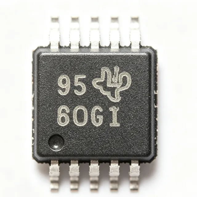
ADS1115IDGSR - 16-Bit I2C ADC with PGA | TI | Sensor Nodes
Артикул: ADS1115IDGSR ✓ Активен| Кол-во | Цена за ед. | Итого |
|---|---|---|
| 1 | $4.36 | $4,36 |
| 10 | $3.95 | $39,50 |
| 100 | $3.52 | $352,00 |
| 500 | $3.1 | $1.550,00 |
| 1.000 | $2.72 | $2.720,00 |
ADS1115IDGSR Обзор
An analog-to-digital converter (ADC) is a mixed-signal device that translates continuous analog voltages into discrete digital codes that microcontrollers and processors can interpret. The ADS1115 operates as a sigma-delta ADC, using oversampling and noise shaping to achieve 16-bit resolution at conversion rates up to 860 samples per second (SPS). Within the signal-chain hierarchy, it belongs to precision data-acquisition ICs and eliminates the need for an external reference or clock source.
Key features include four single-ended or two differential input channels via an input multiplexer, a PGA with gains from 2/3 to 16 V/V, an I2C interface supporting four bus addresses (0x48 through 0x4B), and an onboard comparator with ALERT/conversion-ready output. The device operates from a 2.0V to 5.5V supply over -40C to +125C, drawing only about 150 uA of supply current in continuous mode.
The ADS111x architecture uses a delta-sigma modulator followed by a digital decimation filter for high accuracy at low power. The integrated PGA amplifies small sensor signals before conversion to improve effective resolution, while the low-drift internal reference keeps industrial measurements stable over time and temperature. The lead-free VSSOP-10 package (3.00mm width) suits space-constrained PCB layouts.
Typical applications include battery voltage and current monitoring, portable instrumentation, IoT sensor nodes, temperature and pressure measurement, and industrial process control. Because no external reference or oscillator is required, the ADS1115IDGSR reduces BOM complexity in designs needing 16-bit accuracy on an I2C bus.
For best performance, place a 0.1uF decoupling capacitor close to VDD and use the ADDR pin to avoid I2C bus conflicts. Keep source impedance low enough to charge the sampling capacitor; a low-noise LDO such as TPS7A26-Q1 further improves measurement stability.
Аналоги без доработки для ADS1115IDGSR — тот же корпус, pin-to-pin совместимость. Компоненты в других корпусах, требующие переработки PCB, исключены.
Варианты в этой серии
Модели той же серии, совместимые без доработки с ADS1115IDGSR (тот же форм-фактор и посадочное место) — отличается по Package, Resolution, Architecture, Interface, Number of Input Channels.
Инструмент быстрого сравнения — выберите альтернативные компоненты для сравнения бок о бок:
ADS1115IDGSR-Q1
✅ Прямая замена✓ В наличии
$1.78 / шт.
Открыть даташит →ADS1115QDGSRQ1
✅ Прямая замена📋 Справочный аналог (нет в каталоге)
ADS1114IDGSR
✅ Прямая замена📋 Справочный аналог (нет в каталоге)
ADS1015IDGSR
✅ Прямая замена📋 Справочный аналог (нет в каталоге)
SGM58031XMS10G/TR
✅ Прямая замена📋 Справочный аналог (нет в каталоге)
ADS1115IDGSR Максимальные параметры и электрические характеристики
| Разрешение | 16 bit |
| Converter Type | Delta-Sigma (Sigma-Delta) |
| Number of Channels | 4 (single-ended) / 2 (differential) |
| Частота дискретизации | 8 to 860 SPS |
| Интерфейс | I2C (4 addresses: 0x48 to 0x4B) |
| PGA Gain Settings | 2/3, 1, 2, 4, 8, 16 V/V |
| Input MUX | Integrated 4-channel |
| Voltage Reference | Internal low-drift |
| Oscillator | Internal |
| Comparator | Digital comparator with ALERT/RDY output |
| Напряжение питания | 2.0 V to 5.5 V |
| Рабочая температура | -40C to +125C |
| Корпус | VSSOP-10 (DGS), 3.00 mm width |
| Тип монтажа | Surface Mount |
| Статус RoHS | Compliant |
| Статус жизненного цикла | Active |
Конфигурация выводов ADS1115IDGSR
| Контакт 1 | ADDR — I2C address select (GND=0x48, VDD=0x49, SDA=0x4A, SCL=0x4B) |
| Контакт 2 | ALERT/RDY — Comparator output or conversion-ready |
| Контакт 3 | GND — Ground |
| Контакт 4 | AIN0 — Analog input channel 0 (positive differential input 0) |
| Контакт 5 | AIN1 — Analog input channel 1 (negative differential input 0) |
| Контакт 6 | AIN2 — Analog input channel 2 (positive differential input 1) |
| Контакт 7 | AIN3 — Analog input channel 3 (negative differential input 1) |
| Контакт 8 | SDA — I2C serial data |
| Контакт 9 | SCL — I2C serial clock |
| Контакт 10 | VDD — Power supply, 2.0V to 5.5V |
Типичное применение
ADS1115IDGSR подходит для 6 применениеs: Battery Voltage and Current Monitoring, IoT Sensor Nodes, Portable Instrumentation, Temperature Measurement (Thermocouple/RTD), Industrial Process Control, Power Supply Telemetry.
Battery Voltage and Current Monitoring
The ADS1115IDGSR fits battery monitoring because its differential inputs measure shunt-resistor voltage drops with the PGA at gain 16 (+/-0.256V full scale), resolving microvolt-level signals for precise current calculation, while a second channel tracks pack voltage up to 6.144V input range. Its 2.0V to 5.5V supply matches single-cell Li-ion or 3.3V rails, and single-shot mode with 150uA-class continuous draw preserves battery life. On the PCB, place the device near the shunt with a differential routed pair and use its 16-bit resolution and onboard comparator to trigger an ALERT interrupt on over-current thresholds, removing host polling overhead.
Рекомендуется
IoT Sensor Nodes
IoT nodes use the ADS1115IDGSR to digitize analog sensors (light, gas, pH, soil moisture) over I2C without an external reference or oscillator, cutting BOM count to one IC plus decoupling. Four I2C addresses (0x48-0x4B) allow four ADCs on one bus for up to 16 single-ended channels. Its 16-bit resolution and PGA resolve millivolt-level sensor outputs that would waste resolution on MCU-internal 10-12 bit converters. Single-shot conversion plus power-down between samples suits battery nodes waking periodically; at 860 SPS max rate, firmware should use the conversion-ready ALERT pin rather than fixed delays for deterministic sampling in wireless sensor networks.
Рекомендуется
Portable Instrumentation
Handheld multimeters, data loggers, and environmental meters benefit from the ADS1115IDGSR's combination of 16-bit resolution, low 150uA-class consumption, and 3x3mm-class VSSOP-10 footprint that fits pen-style form factors. The internal low-drift reference maintains calibration across temperature swings encountered in field use, while the PGA gain settings let one input adapt from millivolt thermocouple signals to higher-voltage divider outputs. The differential mode rejects ground noise from LCD backlights and user-interface circuitry. Designers should add RC anti-alias filtering ahead of AINx and exploit single-shot mode to conserve cells between user-triggered measurements.
Рекомендуется
Temperature Measurement (Thermocouple/RTD)
The ADS1115IDGSR converts low-level thermocouple and RTD signals: with PGA gain 16 (+/-0.256V full scale), a Type-K thermocouple's ~41 uV/C output maps across full 16-bit span, giving approximately 4 uV of code width for fine temperature resolution. One channel reads the sensor differentially while another reads a cold-junction sensor such as an analog output LMT84. The internal oscillator and reference remove external clocking, and the ALERT comparator can flag out-of-range temperatures without CPU intervention. Keep the analog front-end source impedance low and add input filtering with large resistors plus small capacitors to survive industrial EMI.
Рекомендуется
Industrial Process Control
In factory automation, the ADS1115IDGSR digitizes 4-20mA loop signals (via a sense resistor), pressure transducer bridges, and potentiometer feedback over the -40C to +125C industrial range. The PGA and differential inputs reject ground offsets across long cable runs, and the wide 6.144V input range at gain 2/3 accommodates divider-scaled 24V-derived signals. The digital comparator with latching ALERT output enables local threshold alarms independent of the host PLC processor. Because the I2C bus tolerates four addresses, several ADS1115 units can aggregate many process channels onto one two-wire bus running to the control board, minimizing wiring.
Рекомендуется
Power Supply Telemetry
The ADS1115IDGSR adds I2C telemetry to power supplies by monitoring output voltage rails through precision dividers and input current through shunts, complementing regulators such as the TPS548B28 or TPS563207 that lack integrated monitors. Its 2.0-5.5V supply connects directly to typical 3.3V housekeeping rails, and the ALERT comparator can flag overvoltage events for fault logging before damage occurs. Use gain 2/3 for 0-5V rails with the divider scaled under 6.144V, and reserve a differential channel for shunt-based current. Add local 0.1uF plus 1uF decoupling and route analog sense traces away from switch-node dV/dt to preserve 16-bit accuracy.
Рекомендуется
Сводка рекомендуемых товаров
Справочные инженерные данные для ADS1115IDGSR — сравнение, рекомендации по проектированию и информация о соответствии.
Руководство по выбору
Сравнение с аналогами
| Параметр | Этот товар | ADS1115IDGSR-Q1 | ADS1115QDGSRQ1 | ADS1114IDGSR | ADS1015IDGSR | SGM58031XMS10G/TR |
|---|---|---|---|---|---|---|
| Package | VSSOP-10 (DGS) | VSSOP-10 (DGS) - same | VSSOP-10 (DGS) - same | VSSOP-10 (DGS) - same | VSSOP-10 (DGS) - same | VSSOP-10 - same footprint |
| Brand | Texas Instruments | Texas Instruments | Texas Instruments | Texas Instruments | Texas Instruments | SGMC (Sagna Microelectronics) |
| Resolution | 16 bit | 16 bit | 16 bit | 16 bit | 12 bit | 16 bit |
| Input Channels | 4 SE / 2 Diff | 4 SE / 2 Diff | 4 SE / 2 Diff | 1 input (no MUX) | 4 SE / 2 Diff | 4 SE / 2 Diff |
| PGA | Yes (2/3 to 16 V/V) | Yes (2/3 to 16 V/V) | Yes (2/3 to 16 V/V) | Yes (2/3 to 16 V/V) | Yes (2/3 to 16 V/V) | Yes |
| AEC-Q100 Qualified | No (industrial grade) | Yes | Yes | No | No | No |
Ключевые отличия
- Integrated 4-channel input MUX (против ADS1114IDGSR)
- 16-bit resolution at lower data rate (против ADS1015IDGSR)
- Drop-in automotive qualified option (против ADS1115QDGSRQ1)
Заметки по проектированию
Place a 0.1uF ceramic decoupling capacitor within 2mm of the VDD pin (pin 10), with a low-impedance ground return to GND (pin 3). Route AIN0-AIN3 as short differential pairs when used differentially, and add an RC filter (e.g., 1k ohm / 10nF) at each input for EMI and anti-aliasing. Keep the I2C traces short with 4.7k to 10k pull-up resistors on SDA/SCL appropriate for bus capacitance.
The input impedance is dynamic because the sampling capacitor charges from the source; source resistance above approximately a few kilo-ohms degrades gain and offset accuracy. Buffer high-impedance sources with an op-amp such as the OPA2375. Also confirm the ADDR pin is tied to a defined rail - a floating ADDR causes bus address conflicts. Do not exceed the absolute maximum input of VDD + 0.3V on AINx pins.
For lowest noise, power the ADS1115IDGSR from a clean low-noise LDO such as the TPS7A26-Q1 rather than a switching regulator output. In battery applications, use single-shot mode with power-down between conversions instead of continuous 860 SPS operation; this reduces average consumption substantially and suits periodic sensor polling on I2C from an MSP430-class host.
Use the conversion-ready (ALERT/RDY) mode rather than fixed-delay polling so conversions are read deterministically at the configured data rate. At 400kHz fast-mode I2C, keep trace length under about 20cm and add series damping resistors if ringing is observed. Separate analog ground for the input filters from switching-regulator return paths to protect the 16-bit noise floor.
Информация о соответствии
RoHS compliant per TI product data; VSSOP-10 package is lead-free. Use ADS1115QDGSRQ1 for AEC-Q100 automotive applications.







