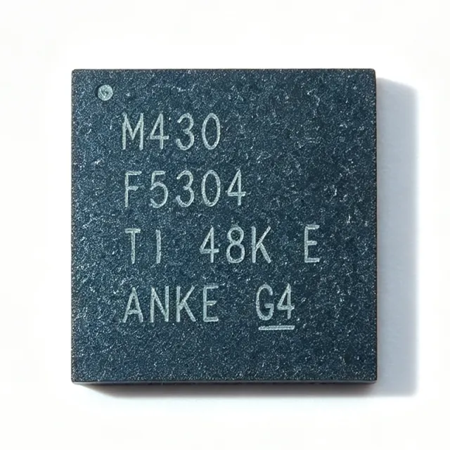
MSP430F5304IPTR - 16-bit 25MHz 8KB Flash MCU | Texas Instruments
Артикул: MSP430F5304IPTR ✓ Активен| Кол-во | Цена за ед. | Итого |
|---|---|---|
| 1 | $3.45 | $3,45 |
| 10 | $3.1 | $31,00 |
| 100 | $2.72 | $272,00 |
| 500 | $2.38 | $1.190,00 |
| 1.000 | $2.1 | $2.100,00 |
MSP430F5304IPTR Обзор
An ultra-low-power microcontroller (MCU) is a single-chip processor optimized to minimize active and standby current draw, essential for battery-operated and energy-harvesting systems. The MSP430 family sits within the broader hierarchy of 16-bit microcontrollers -> mixed-signal MCUs -> embedded processors, and is widely recognized as an industry benchmark for low-power design.
Key features include the flexible clock system (5 selectable low-power modes), a hardware 32x32 multiplier that offloads arithmetic from the CPU, and DMA for peripheral-to-memory transfers without CPU intervention. The integrated LDO simplifies power tree design by generating the core supply from a single external rail, while the RTC with alarm supports timekeeping during standby. The 10-bit ADC provides general-purpose analog acquisition for sensor front ends.
The MSP430F5xx architecture pairs the von Neumann CPUXV2 core with a clock system supporting a VLO, REFO, XT1, and DCO sources, allowing designers to trade clock accuracy against current consumption. Interrupt-driven operation with fast wake-up keeps average current in the microamp range in duty-cycled applications.
Typical applications include battery-powered metering, portable medical monitoring, industrial sensor nodes, and consumer appliances where the combination of 25 MHz performance, one USCI serial port, and 31 GPIO covers most moderate-complexity control tasks.
Design consideration: the family shares the MSP430F5xx/F6xx User's Guide peripheral set, so code migrates freely between family members; verify Flash/SRAM sizing and package pinout before board reuse, as memory-density variants exist in identical footprints.
Аналоги без доработки для MSP430F5304IPTR — тот же корпус, pin-to-pin совместимость. Компоненты в других корпусах, требующие переработки PCB, исключены.
Инструмент быстрого сравнения — выберите альтернативные компоненты для сравнения бок о бок:
MSP430F5308IPTR
📋 Справочный аналог (нет в каталоге)
MSP430F5309IPTR
📋 Справочный аналог (нет в каталоге)
MSP430F5310IPTR
📋 Справочный аналог (нет в каталоге)
MSP430F5304IRGZR
📋 Справочный аналог (нет в каталоге)
MSP430F5304IPT
📋 Справочный аналог (нет в каталоге)
MSP430F5304IPTR Максимальные параметры и электрические характеристики
| Core | MSP430 CPUXV2, 16-bit |
| Максимальная тактовая частота | 25 MHz |
| Flash Memory | 8 KB (8K x 8) |
| SRAM | 6 KB |
| ADC Resolution | 10-bit |
| Timers | 4 x 16-bit |
| Communication Interfaces | 1 x USCI (UART/SPI/I2C) |
| DMA Channels | Yes (DMA controller) |
| Hardware Multiplier | Yes (32-bit) |
| RTC | RTC with alarm capabilities |
| Integrated LDO | 3.3 V |
| I/O Pins | 31 |
| Рабочая температура | -40C to +85C (I grade) |
| Корпус | 48-LQFP (7x7 mm) |
| Тип монтажа | Surface Mount |
| Family | MSP430F5xx |
Конфигурация выводов MSP430F5304IPTR
| Контакт 1 | P1.0/TA0CLK/ACLK — GPIO Port 1 / Timer A0 clock input |
| Контакт 4 | PJ.0/XIN — Crystal input / general I/O |
| Контакт 5 | PJ.1/XOUT — Crystal output / general I/O |
| Контакт 13 | DVCC1 — Digital supply (3.3V) |
| Контакт 14 | DVSS1 — Digital ground |
| Контакт 24 | P6.0/A0 — GPIO / ADC input channel 0 |
| Контакт 25 | P6.1/A1 — GPIO / ADC input channel 1 |
| Контакт 31 | RST/NMI — Reset or non-maskable interrupt input |
| Контакт 38 | TEST/SBWTCK — Test mode / Spy-Bi-Wire clock for programming |
| Контакт 48 | DVCC3 — Digital supply pin 3 |
Типичное применение
MSP430F5304IPTR подходит для 6 применениеs: Battery-Powered Metering, Portable Medical Monitoring, Industrial Sensor Nodes, Building Automation Controls, Consumer Appliance Control, Data Loggers.
Battery-Powered Metering
Utility and energy meters benefit directly from the MSP430F5304's ultra-low-power architecture. The 25 MHz CPUXV2 core handles metering computation using the hardware 32-bit multiplier for energy calculations, while the RTC with alarm maintains time-of-use records in standby. Duty-cycled firmware using LPM3 keeps average current in the microamp range; the 8KB Flash is sufficient for fixed-function metering firmware, and the 10-bit ADC samples sensor or shunt inputs for energy measurement.
Рекомендуется
Portable Medical Monitoring
Wearable and portable medical devices require long battery life and reliable analog acquisition. The MSP430F5304's 10-bit ADC digitizes biopotential or temperature front ends, the one USCI streams data over UART/SPI/I2C to a wireless module or display, and four 16-bit timers generate precisely timed sampling intervals. The integrated 3.3V LDO accepts a single lithium-cell-derived rail, and the I-grade -40C to +85C range covers storage and transport conditions.
Рекомендуется
Industrial Sensor Nodes
Factory sensor nodes use the MSP430F5304 as an energy-conscious hub: the DMA moves ADC samples to SRAM without CPU intervention, timers generate PWM or wake-up intervals, and the USCI provides I2C/SPI links to local sensors or RS-485 bridges. The RTC with alarm supports scheduled wake-and-report duty cycles, and 31 GPIO handles relay, LED, and switch interfacing in a single 7x7 mm 48-pin package.
Рекомендуется
Building Automation Controls
Thermostats, dampers, and occupancy-driven controls map well onto the MSP430F5304. The 8KB Flash holds control and scheduling logic, the RTC with alarm executes setpoint schedules across power cycles, the 10-bit ADC reads potentiometer or NTC inputs, and the USCI talks to display or network coprocessors. Multiple low-power modes let the unit sit idle between occupancy events, minimizing HVAC controller standby draw.
Рекомендуется
Consumer Appliance Control
Appliance front panels and simple control boards use the MSP430F5304 for key scanning, LED indication, and motor or heater sequencing. The 25 MHz CPU delivers responsive user-interface behavior, the hardware multiplier accelerates scaling math for sensor linearization, and four 16-bit timers provide PWM channels for fan or heater control. The single-supply design with the integrated LDO keeps the power section to one rail plus decoupling.
Рекомендуется
Data Loggers
Standalone loggers record periodic sensor samples to memory over long deployment periods. The MSP430F5304's DMA fills an SRAM buffer from the 10-bit ADC while the CPU sleeps, the RTC timestamps each record, and the USCI offloads buffered data over SPI to Flash memory such as W25Q64JVSSIG or over UART to a host. Wake-on-interval firmware keeps average current low enough for multi-year operation from a primary cell.
Рекомендуется
Сводка рекомендуемых товаров
Справочные инженерные данные для MSP430F5304IPTR — сравнение, рекомендации по проектированию и информация о соответствии.
Руководство по выбору
Сравнение с аналогами
| Параметр | Этот товар | MSP430F5308IPTR | MSP430F5309IPTR | MSP430F5310IPTR | MSP430F5304IRGZR |
|---|---|---|---|---|---|
| Package | 48-LQFP (7x7) | 48-LQFP (7x7) - same | 48-LQFP (7x7) - same | 48-LQFP (7x7) - same | 48-VQFN (7x7) - different footprint |
| Brand | Texas Instruments | Texas Instruments | Texas Instruments | Texas Instruments | Texas Instruments |
| Flash Memory | 8 KB | 16 KB | 32 KB | 32 KB | 8 KB |
| SRAM | 6 KB | 6 KB | 6 KB | 10 KB | 6 KB |
| Max Clock Frequency | 25 MHz | 25 MHz | 25 MHz | 25 MHz | 25 MHz |
| USCI Modules | 1 | 1 | 1 | 2 | 1 |
| ADC | 10-bit | 10-bit | 10-bit | 10-bit | 10-bit |
| Integrated LDO | Yes (3.3V) | Yes (3.3V) | Yes (3.3V) | Yes (3.3V) | Yes (3.3V) |
| Temperature Grade | I (-40C to +85C) | I (-40C to +85C) | I (-40C to +85C) | I (-40C to +85C) | I (-40C to +85C) |
Ключевые отличия
- Lowest cost/memory in F530x subfamily (против MSP430F5309IPTR)
- Integrated 3.3V LDO eliminates external core regulator (против MSP430F5310IPTR)
- 48-LQFP eases hand assembly and inspection (против MSP430F5304IRGZR)
Заметки по проектированию
The MSP430F5304 integrates a 3.3V LDO/PMM core regulator, so a single external rail powers DVCC pins. Decouple every DVCC pin (1, 48) with 100nF placed within 2mm, plus a 4.7uF bulk capacitor. Do not drive the VCORE node externally - the LDO output requires only its datasheet-specified capacitor. Per the TI MSP430 Hardware Design Guide (SLAU278), never leave DVSS pins unconnected.
Route the RST/NMI pin (pin 31) with a 47k pullup and optional 10nF to ground for noise immunity; this pin also serves as the Spy-Bi-Wire programming interface together with TEST/SBWTCK (pin 38). Provide a 2x1 header on these pins plus DVCC/DVSS in every layout to allow in-circuit programming and debug without board rework.
Verify Flash size headroom before finalizing BOM: 8KB is the smallest configuration in the F530x subfamily. If C code grows past ~7KB, move to the pin-compatible MSP430F5308/F5309 instead of optimizing away features. Also confirm the one-USCI budget - designs needing simultaneous UART plus SPI or I2C must use MSP430F5310 (two USCI) or bit-bang the second interface.
Информация о соответствии
RoHS/compliant and lead-free per TI standard product offering; REACH and halogen-free status should be confirmed on the TI product page.


