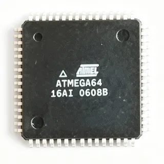
ATMEGA32-16AC - 8-bit AVR MCU 16MHz 32KB Flash | Microchip
Артикул: ATMEGA32-16AC ✓ Активен| Кол-во | Цена за ед. | Итого |
|---|---|---|
| 1 | $6.9 | $6,90 |
| 10 | $6.21 | $62,10 |
| 100 | $5.52 | $552,00 |
| 500 | $4.97 | $2.485,00 |
| 1.000 | $4.48 | $4.480,00 |
ATMEGA32-16AC Обзор
A microcontroller (MCU) is a single integrated circuit that combines a processor core, program memory, data memory, and peripherals such as timers, UARTs, and ADCs into one chip. The ATmega32 belongs to the AVR family of enhanced RISC microcontrollers, positioned within the broader embedded processor hierarchy beneath 32-bit ARM MCUs, and is a classic member of the 8-bit microcontroller class used throughout industrial and consumer electronics.
Key features include 131 powerful instructions with mostly single-cycle execution, 32 general-purpose working registers, an 8-channel 10-bit ADC, a JTAG interface for on-chip debugging and boundary scan, and self-programming Flash enabling boot-loader based field updates. These peripherals allow a single ATmega32 to replace multi-chip analog-and-logic designs.
Architecturally, the AVR core uses a Harvard structure with separate program and data buses, so instruction fetch and data access occur in parallel. With most instructions executing in a single clock cycle, the device achieves close to 1 MIPS per MHz, letting designers run at lower clock frequencies for reduced power while maintaining throughput. Operating voltage is 4.5 V to 5.5 V, making the -16AC grade well matched to 5 V industrial logic levels.
Typical applications include industrial control panels, HVAC and building automation, motor control front ends, and 5 V legacy instrumentation where the 10-bit ADC, two 8-bit timers, one 16-bit timer, USART, SPI, and TWI (I2C) interfaces cover the full sensing and communication need of a compact controller.
A key design consideration is that the -16AC grade specifies operation at 4.5 V to 5.5 V; designs needing 2.7 V to 5.5 V operation should select the ATmega32L variant. Decouple VCC and AVCC separately with 100 nF capacitors placed close to the pins.
This page synthesizes verified distributor data, drop-in alternatives, pinout information, and practical design notes in one place - information not consolidated in the manufacturer datasheet alone.
Аналоги без доработки для ATMEGA32-16AC — тот же корпус, pin-to-pin совместимость. Компоненты в других корпусах, требующие переработки PCB, исключены.
Варианты в этой серии
Модели той же серии, совместимые без доработки с ATMEGA32-16AC (тот же форм-фактор и посадочное место) — отличается по Package, SRAM, Core Architecture, Debug Interface, EEPROM.
Инструмент быстрого сравнения — выберите альтернативные компоненты для сравнения бок о бок:
ATMEGA32A-AU
✅ Прямая замена✓ В наличии
$2.95 / шт.
Открыть даташит →ATMEGA32-16AU
✅ Прямая замена📋 Справочный аналог (нет в каталоге)
ATMEGA16A-AU
✅ Прямая замена ⚠️ Характеристики не проверены✓ В наличии
$2.05 / шт.
Открыть даташит →ATMEGA8535-16AU
✅ Прямая замена✓ В наличии
$4.41 / шт.
Открыть даташит →ATMEGA324PA-AU
✅ Прямая замена ⚠️ Характеристики не проверены✓ В наличии
$2.87 / шт.
Открыть даташит →ATMEGA32-16AC Максимальные параметры и электрические характеристики
| Core Architecture | 8-bit AVR RISC |
| Flash Program Memory | 32 KB (16K x 16) |
| SRAM | 2 KB |
| EEPROM | 1 KB |
| Максимальная тактовая частота | 16 MHz |
| Throughput | 16 MIPS at 16 MHz |
| Operating Voltage Range | 4.5 V to 5.5 V |
| ADC Resolution | 10-bit |
| ADC Channels | 8 channels |
| Number of I/O Pins | 32 |
| Timers | Two 8-bit, one 16-bit |
| Communication Interfaces | USART, SPI, TWI (I2C) |
| Debug Interface | JTAG (on-chip debug, boundary scan) |
| Корпус | 44-TQFP (10 x 10 mm) |
| Тип монтажа | Surface Mount |
| Instructions | 131 instructions, most single-cycle |
| Product Family | AVR ATmega |
Конфигурация выводов ATMEGA32-16AC
| Контакт 1 | PA0 (ADC0) — Port A bit 0 / ADC channel 0 |
| Контакт 2 | PA1 (ADC1) — Port A bit 1 / ADC channel 1 |
| Контакт 3 | PA2 (ADC2) — Port A bit 2 / ADC channel 2 |
| Контакт 4 | PA3 (ADC3) — Port A bit 3 / ADC channel 3 |
| Контакт 5 | PA4 (ADC4) — Port A bit 4 / ADC channel 4 |
| Контакт 6 | PA5 (ADC5) — Port A bit 5 / ADC channel 5 |
| Контакт 7 | PA6 (ADC6) — Port A bit 6 / ADC channel 6 |
| Контакт 8 | PA7 (ADC7) — Port A bit 7 / ADC channel 7 |
| Контакт 9 | VCC — Digital supply voltage |
| Контакт 10 | GND — Ground |
| Контакт 11 | PB7 (OC2/OC1C) — Port B bit 7 / Timer2 output compare |
| Контакт 12 | PB6 (OC1B) — Port B bit 6 / Timer1 output compare B |
| Контакт 13 | PB5 (OC1A) — Port B bit 5 / Timer1 output compare A |
| Контакт 14 | PB4 (OC0) — Port B bit 4 / Timer0 output compare |
| Контакт 15 | PB3 (AIN1) — Port B bit 3 / Analog comparator negative input |
| Контакт 16 | PB2 (AIN0/INT2) — Port B bit 2 / Comparator positive input / External interrupt 2 |
| Контакт 17 | PB1 (T1) — Port B bit 1 / Timer1 external counter input |
| Контакт 18 | PB0 (XCK/T0) — Port B bit 0 / USART external clock / Timer0 counter input |
| Контакт 19 | PD7 (OC2) — Port D bit 7 / Timer2 output compare |
| Контакт 20 | PD6 (ICP1) — Port D bit 6 / Timer1 input capture |
| Контакт 21 | PD5 (OC1A) — Port D bit 5 / Timer1 output compare A |
| Контакт 22 | PD4 (OC1B) — Port D bit 4 / Timer1 output compare B |
| Контакт 23 | PD3 (INT1) — Port D bit 3 / External interrupt 1 |
| Контакт 24 | PD2 (INT0) — Port D bit 2 / External interrupt 0 |
| Контакт 25 | PD1 (TXD) — Port D bit 1 / USART transmit |
| Контакт 26 | PD0 (RXD) — Port D bit 0 / USART receive |
| Контакт 27 | PC7 (TCK) — Port C bit 7 / JTAG test clock |
| Контакт 28 | PC6 (TMS) — Port C bit 6 / JTAG test mode select |
| Контакт 29 | PC5 (TDO) — Port C bit 5 / JTAG test data output |
| Контакт 30 | PC4 (TDI) — Port C bit 4 / JTAG test data input |
| Контакт 31 | PC3 (TOSC2) — Port C bit 3 / Timer oscillator output |
| Контакт 32 | PC2 (TOSC1) — Port C bit 2 / Timer oscillator input |
| Контакт 33 | PC1 (SDA) — Port C bit 1 / TWI data |
| Контакт 34 | PC0 (SCL) — Port C bit 0 / TWI clock |
| Контакт 35 | VCC — Digital supply voltage |
| Контакт 36 | GND — Ground |
| Контакт 37 | AREF — ADC reference voltage |
| Контакт 38 | AVCC — ADC supply voltage |
| Контакт 39 | RESET — Reset input (active low) |
| Контакт 40 | XTAL1 — Crystal/oscillator input |
| Контакт 41 | XTAL2 — Crystal/oscillator output |
| Контакт 42 | GND — Ground |
| Контакт 43 | AVCC — ADC supply voltage |
| Контакт 44 | AREF — ADC reference voltage |
Типичное применение
ATMEGA32-16AC подходит для 6 применениеs: Industrial Control Panels, Analog Data Acquisition, HVAC and Building Automation, Motor Control Front Ends, 5V Legacy Instrumentation Maintenance, Educational and Embedded Prototyping.
Industrial Control Panels
The ATMEGA32-16AC fits industrial control panels because its 4.5 V to 5.5 V operating range matches legacy 5 V PLC-style logic directly, and its 32 KB flash is large enough for PID loops, state machines, and HMI communication firmware. Per the datasheet, the JTAG interface supports on-chip debugging, which shortens commissioning of panel logic. Typical usage places the MCU at the center of a relay/timer/counter board, using the USART (RXD/TXD pins) for Modbus-style serial links and the 16-bit Timer/Counter1 for precise timing. Because instructions mostly execute in one cycle, deterministic I/O response is achieved without RTOS overhead; the trade-off is that 5 V operation raises power versus 3.3 V MCUs, so board dissipation should be budgeted.
Рекомендуется
Analog Data Acquisition
With an 8-channel 10-bit ADC multiplexed onto Port A (pins 1-8), the ATMEGA32-16AC serves as a complete low-cost data acquisition front end for temperature, pressure, and voltage sensing. Per the datasheet, the ADC supports a reference from AREF (pin 37) or AVCC (pin 38), enabling 4.88 mV resolution on a 5 V reference; the 1 KB EEPROM stores calibration constants across power cycles. Designers typically sample channels sequentially with the built-in prescaler and stream results over USART or SPI. Performance consideration: ADC accuracy degrades if digital port switching injects noise into AVCC, so a separate LC filter on AVCC is recommended. The 2 KB SRAM comfortably buffers sample blocks for averaging before transmission.
Рекомендуется
HVAC and Building Automation
Building automation nodes benefit from the ATMEGA32-16AC combination of 32 programmable I/O lines, TWI (I2C) on Port C for sensor expansion, and 5 V noise immunity suited to electrically harsh plant rooms. The TWI interface (SDA/SCL on PC1/PC0) connects RTCs, EEPROMs, and humidity sensors, while Timer/Counter PWM outputs (OC0, OC1A, OC1B, OC2) drive damper actuators and fan speed control. Firmware for scheduling and communication fits within 32 KB flash with room for boot-loader updates via the self-programming flash feature. Per the datasheet, the JTAG boundary-scan capability aids production test of assembled boards. For outdoor or unheated enclosures, choose the industrial-grade ATMEGA32-16AU which shares the identical footprint.
Рекомендуется
Motor Control Front Ends
The ATMEGA32-16AC provides the timing resources needed for small motor control: one 16-bit timer (Timer1) with two compare outputs (OC1A on PD5, OC1B on PD4) plus two 8-bit timers, enabling multi-channel PWM generation for DC and stepper motor drivers. The input capture pin (ICP1, PD6) permits precise measurement of tachometer or encoder periods, closing speed loops in software. Its 16 MIPS at 16 MHz throughput, per the datasheet, leaves adequate headroom for PI control at several-kilohertz loop rates. Design consideration: the MCU cannot drive motors directly - pair it with an H-bridge driver such as the L298 or MOSFET pre-drivers, and use the 10-bit ADC channel on PA0-PA7 for current-sense feedback through a shunt amplifier.
Рекомендуется
5V Legacy Instrumentation Maintenance
Service and maintenance of existing 5 V instruments is a primary remaining use case for the original ATmega32 die. The ATMEGA32-16AC keeps old designs serviceable with the exact original component, avoiding any requalification that a die-shrunk substitute might trigger. Its JTAG interface (TCK/TMS/TDO/TDI on PC7-PC4) allows re-flashing and on-chip-debug of boards already installed in the field when the self-programming boot loader is present. Per the datasheet, boundary-scan through the same JTAG port verifies board interconnects after repair. When stocks of the -16AC run out, the ATMEGA32A-AU is the verified drop-in successor, matching the 44-TQFP footprint and all electrical specifications of the original.
Рекомендуется
Educational and Embedded Prototyping
The ATmega32 remains a staple of embedded-systems education because it exposes every classic MCU subsystem - GPIO, timers, ADC, UART, SPI, I2C, and external interrupts (INT0/INT1/INT2 on PD2, PD3, PB2) - in a single 44-TQFP device with free toolchains and abundant course material. The 32 KB flash provides generous space for student projects, and in-system programming through the SPI pins (MISO/MOSI/SCK on PB6/PB5/PB7) needs only a low-cost ISP programmer. Per the datasheet, the JTAG OCD interface also supports step debugging in AVR Studio-based flows. Its 5 V operation simplifies breadboard use with 5 V peripherals; students should still decouple AVCC separately for clean ADC experiments.
Рекомендуется
Сводка рекомендуемых товаров
Справочные инженерные данные для ATMEGA32-16AC — сравнение, рекомендации по проектированию и информация о соответствии.
Руководство по выбору
Сравнение с аналогами
| Параметр | Этот товар | ATMEGA32A-AU | ATMEGA32-16AU | ATMEGA16A-AU | ATMEGA8535-16AU |
|---|---|---|---|---|---|
| Package | 44-TQFP (10 x 10 mm) | 44-TQFP (10 x 10 mm) - same | 44-TQFP (10 x 10 mm) - same | 44-TQFP (10 x 10 mm) - same | 44-TQFP (10 x 10 mm) - same |
| Brand | Microchip Technology (Atmel) | Microchip Technology | Microchip Technology | Microchip Technology | Microchip Technology |
| Flash Memory | 32 KB | 32 KB | 32 KB | 16 KB | 8 KB |
| SRAM | 2 KB | 2 KB | 2 KB | 1 KB | 512 B |
| EEPROM | 1 KB | 1 KB | 1 KB | 512 B | 512 B |
| Max Clock Frequency | 16 MHz | 16 MHz | 16 MHz | 16 MHz | 16 MHz |
| Operating Voltage | 4.5 V to 5.5 V | 4.5 V to 5.5 V | 4.5 V to 5.5 V | 4.5 V to 5.5 V (16 MHz grade) | 4.5 V to 5.5 V |
| Operating Temperature | Commercial grade (0C to +70C) | -40C to +85C | -40C to +85C | -40C to +85C | -40C to +85C |
| 10-bit ADC Channels | 8 | 8 | 8 | 8 | 8 |
| JTAG Debug | Yes | Yes | Yes | Yes | Yes |
Ключевые отличия
- Full 32 KB flash with pin-compatible shrink path (против ATMEGA16A-AU)
- Original-die availability for legacy requalification (против ATMEGA32A-AU)
- Commercial-grade cost advantage (против ATMEGA32-16AU)
- More memory than same-package ATmega8535 (против ATMEGA8535-16AU)
Заметки по проектированию
Decouple both VCC pairs (pins 9 and 35) with 100 nF ceramic capacitors placed within 5 mm of each pin, plus one 4.7 uF bulk capacitor per board. AVCC (pins 38/43) must be connected to VCC even if the ADC is unused, per the datasheet, but route it through a 10 uH inductor or ferrite bead with a separate 100 nF decoupler to keep digital switching noise out of ADC reference path. Keep AREF (pins 37/44) decoupled with 100 nF to ground and never drive it directly from a low-impedance source without a series resistor.
JTAG is enabled by default on Port C (pins PC4-PC7), which means PC4-PC7 cannot be used as general-purpose I/O until the JTAGEN fuse is disabled. Many designs fail at bring-up because outputs on Port C appear stuck. If JTAG debugging is not needed, clear the JTAGEN fuse via ISP programming; alternatively the JTD bit in MCUCSR can disable JTAG in software after two write cycles within four cycles, per the datasheet. Also remember RESET (pin 39) needs a 10 kOhm pull-up for reliable ISP programming when external circuitry loads the pin.
The -16AC grade requires 4.5 V minimum for guaranteed 16 MHz operation; designs powered from a marginal 5 V rail (e.g., long cables or diode-dropped supplies) should measure worst-case rail voltage under full load. Estimated: at 16 MHz with typical toggling I/O, core current is roughly 15-25 mA per family datasheet curves, so total board draw including I/O loads determines regulator sizing. Brown-out detection (BOD fuse) at 4.0 V is recommended to prevent flash corruption during slow power-down - enable BODLEVEL appropriately for a 5 V system.
Route XTAL1/XTAL2 (pins 40/41) crystal traces short and symmetric, with the crystal ground shields returned directly to the nearest GND pin (10 or 42). Keep clock traces away from ADC input traces on Port A to minimize crosstalk into conversions. For USART runs longer than a few tens of centimeters, add RS-485/RS-232 transceivers rather than driving TTL levels off-board. Underside of the TQFP has no exposed pad on this package, so thermal relief is straightforward but copper pours under the part still aid noise reduction.
Информация о соответствии
The original ATmega32 (non-A) die predates later green/RoHS packaging rollouts; RoHS/REACH status for the -16AC suffix must be confirmed from the official Microchip product page or certificate of conformance. The newer ATMEGA32A-AU is the RoHS-oriented replacement.