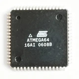
ATMEGA8535L-8AJ - 8KB AVR MCU, 8MHz, TQFP-44 | Microchip
Артикул: ATMEGA8535L-8AJ ✓ Активен| Кол-во | Цена за ед. | Итого |
|---|---|---|
| 1 | $4.2 | $4,20 |
| 10 | $3.78 | $37,80 |
| 100 | $3.36 | $336,00 |
| 500 | $3.02 | $1.510,00 |
| 1.000 | $2.7 | $2.700,00 |
ATMEGA8535L-8AJ Обзор
An 8-bit microcontroller (MCU) is a single-chip computer that integrates a processor core, program memory, data memory, and peripherals on one die. In the embedded-systems hierarchy, an MCU sits above discrete logic and below application processors, providing self-contained control for sensors, actuators, and human-machine interfaces.
Key features of the ATMEGA8535L include the AVR advanced RISC architecture with 130 powerful instructions, most executing in a single clock cycle, and 32 general-purpose working registers. The core delivers up to 16 MIPS throughput at 16MHz, so at the 8MHz limit of this L-grade part it still reaches roughly 8 MIPS. Communication peripherals include a byte-oriented Two-wire Serial Interface (I2C/TWI), an SPI interface, and a programmable USART (UART), covering virtually all common embedded buses.
The peripheral set comprises three flexible Timer/Counters with compare and PWM modes, internal and external interrupt sources, a watchdog timer, and the 8-channel 10-bit analog-to-digital converter with internal reference options, plus 32 general-purpose I/O lines. In-System Self-Programming of the Flash with Read-While-Write support enables field firmware updates without a socketed device.
Typical applications include industrial control panels, battery-powered instruments (leveraging the 2.7V low-voltage operation and low-power idle/power-down modes), sensor data acquisition front ends using the 8-channel ADC, and motor control or lighting systems using the PWM timer outputs.
Design consideration: the 8MHz clock ceiling of this L-grade device is the trade-off for 2.7V operation; if your design runs at 5V and needs 16MHz, choose the ATMEGA8535-16A variants instead.
This page synthesizes verified distributor inventory data, drop-in alternatives, and practical design guidance not found in a single manufacturer datasheet.
Аналоги без доработки для ATMEGA8535L-8AJ — тот же корпус, pin-to-pin совместимость. Компоненты в других корпусах, требующие переработки PCB, исключены.
Варианты в этой серии
Модели той же серии, совместимые без доработки с ATMEGA8535L-8AJ (тот же форм-фактор и посадочное место) — отличается по Throughput, Package, RoHS Status, Core Architecture, Instructions.
Инструмент быстрого сравнения — выберите альтернативные компоненты для сравнения бок о бок:
ATMEGA8535-16AU
✅ Прямая замена✓ В наличии
$4.41 / шт.
Открыть даташит →ATMEGA8535-16AI
✅ Прямая замена ⚠️ Характеристики не проверены📋 Справочный аналог (нет в каталоге)
ATMEGA8535L-8AI
✅ Прямая замена ⚠️ Характеристики не проверены📋 Справочный аналог (нет в каталоге)
ATMEGA8515L-8AI
✅ Прямая замена✓ В наличии
$2.05 / шт.
Открыть даташит →ATMEGA8515L-8AUR
✅ Прямая замена✓ В наличии
$1.98 / шт.
Открыть даташит →ATMEGA8535L-8AJ Максимальные параметры и электрические характеристики
| Core | 8-bit AVR RISC |
| Core Speed | 8 MHz (L-grade maximum) |
| Flash Program Memory | 8 KB (4K x 16) In-System Self-Programmable |
| SRAM | 512 bytes |
| EEPROM | 512 bytes |
| ADC | 8-channel, 10-bit |
| GPIO Count | 32 |
| Communication Interfaces | I2C (TWI), SPI, UART/USART |
| Timers | Three Timer/Counters with compare modes |
| Operating Voltage Range | 2.7 V to 5.5 V (L suffix) |
| Рабочая температура | -40C to +85C (industrial, J suffix) |
| Instructions | 130 instructions, most single-cycle |
| Корпус | 44-TQFP (10 x 10 mm) |
| Тип монтажа | Surface Mount |
| Throughput | Up to 16 MIPS at 16 MHz (family rating) |
| Статус RoHS | Compliant |
Конфигурация выводов ATMEGA8535L-8AJ
| Контакт 1 | PA0 (ADC0) — Port A bit 0 / ADC channel 0 |
| Контакт 2 | PA1 (ADC1) — Port A bit 1 / ADC channel 1 |
| Контакт 3 | PA2 (ADC2) — Port A bit 2 / ADC channel 2 |
| Контакт 4 | PA3 (ADC3) — Port A bit 3 / ADC channel 3 |
| Контакт 5 | PA4 (ADC4) — Port A bit 4 / ADC channel 4 |
| Контакт 6 | PA5 (ADC5) — Port A bit 5 / ADC channel 5 |
| Контакт 7 | PA6 (ADC6) — Port A bit 6 / ADC channel 6 |
| Контакт 8 | PA7 (ADC7) — Port A bit 7 / ADC channel 7 |
| Контакт 9 | PE0 (RXD/PDI) — Port E bit 0 / USART receive / programming data input |
| Контакт 10 | PE1 (TXD/PDO) — Port E bit 1 / USART transmit / programming data output |
| Контакт 11 | PB0 (XCK/T0) — Port B bit 0 / USART external clock / Timer0 external clock |
| Контакт 12 | PB1 (T1) — Port B bit 1 / Timer1 external clock |
| Контакт 13 | PB2 (AIN0/INT2) — Port B bit 2 / analog comparator input 0 / external interrupt 2 |
| Контакт 14 | PB3 (AIN1/OC0) — Port B bit 3 / analog comparator input 1 / Timer0 output compare |
| Контакт 15 | PB4 (SS) — Port B bit 4 / SPI slave select |
| Контакт 16 | PB5 (MOSI) — Port B bit 5 / SPI master output |
| Контакт 17 | PB6 (MISO) — Port B bit 6 / SPI master input |
| Контакт 18 | PB7 (SCK/OC2) — Port B bit 7 / SPI clock / Timer2 output compare |
| Контакт 19 | VCC — Digital supply voltage |
| Контакт 20 | GND — Ground |
| Контакт 21 | RESET — Reset input (active low) |
| Контакт 22 | XTAL2 — Oscillator output |
| Контакт 23 | XTAL1 — Oscillator input |
| Контакт 24 | AVCC — ADC supply voltage |
| Контакт 25 | AREF — ADC reference voltage |
| Контакт 26 | GND — Ground |
| Контакт 27 | PC0 (SCL) — Port C bit 0 / TWI clock |
| Контакт 28 | PC1 (SDA) — Port C bit 1 / TWI data |
| Контакт 29 | PC2 (TCK) — Port C bit 2 / JTAG test clock |
| Контакт 30 | PC3 (TMS) — Port C bit 3 / JTAG test mode select |
| Контакт 31 | PC4 (TDO) — Port C bit 4 / JTAG test data output |
| Контакт 32 | PC5 (TDI) — Port C bit 5 / JTAG test data input |
| Контакт 33 | PC6 (TOSC1) — Port C bit 6 / Timer oscillator input |
| Контакт 34 | PC7 (TOSC2) — Port C bit 7 / Timer oscillator output |
| Контакт 35 | PD0 — Port D bit 0 |
| Контакт 36 | PD1 — Port D bit 1 |
| Контакт 37 | PD2 (INT0) — Port D bit 2 / external interrupt 0 |
| Контакт 38 | PD3 (INT1) — Port D bit 3 / external interrupt 1 |
| Контакт 39 | PD4 (OC1B) — Port D bit 4 / Timer1 output compare B |
| Контакт 40 | PD5 (OC1A) — Port D bit 5 / Timer1 output compare A |
| Контакт 41 | PD6 (ICP1) — Port D bit 6 / Timer1 input capture |
| Контакт 42 | PD7 — Port D bit 7 |
| Контакт 43 | VCC — Digital supply voltage |
| Контакт 44 | GND — Ground |
Типичное применение
ATMEGA8535L-8AJ подходит для 6 применениеs: Industrial Control Systems, Battery-Powered Instruments, Multi-Channel Analog Data Acquisition, PWM Motor and Lighting Control, Embedded Communication Bridges, Legacy AVR System Sustenance.
Industrial Control Systems
The ATMEGA8535L-8AJ fits industrial control panels and PLC-style I/O modules because it combines 32 GPIO lines, three Timer/Counters with compare modes, and both external and internal interrupt sources in one 44-TQFP device. Its industrial -40C to +85C temperature rating and I2C/SPI/USART set allow direct interfacing with relays, encoders, HMI displays, and Modbus-style UART links. The AVR core's single-cycle execution gives roughly 8 MIPS at 8MHz, sufficient for deterministic scan loops. Running from a 5V industrial rail provides noise margin, while the 2.7V floor permits low-voltage control electronics when needed.
Рекомендуется
Battery-Powered Instruments
The L-grade 2.7V to 5.5V operating range of the ATMEGA8535L-8AJ makes it well suited to battery-powered handheld meters and dataloggers. The AVR architecture offers low-power idle and power-down sleep modes, and the 512-byte EEPROM retains calibration constants across battery replacement without external NVRAM. An 8MHz clock ceiling keeps dynamic current low, and the integrated 10-bit ADC eliminates a separate converter IC, reducing BOM cost and quiescent drain. Designers typically clock from a watch crystal in sleep and the internal 8MHz RC during active measurement to balance precision against power.
Рекомендуется
Multi-Channel Analog Data Acquisition
With an 8-channel 10-bit ADC multiplexed onto PORTA and an internal reference option, the ATMEGA8535L-8AJ can digitize up to eight analog sensor inputs without external conversion hardware. Typical uses include temperature arrays, pressure monitoring, and voltage-scan front ends where 10-bit resolution (roughly 4.9 mV LSB at 5V reference) is adequate. Successive-approximation conversion supports free-running or single-shot modes under Timer/Counter or interrupt control, letting firmware synchronize sampling with process events. SPI then streams results to external memory or a host, while TWI interfaces digital sensors on the same bus.
Рекомендуется
PWM Motor and Lighting Control
Three Timer/Counters with compare modes generate multiple PWM channels directly from the ATMEGA8535L-8AJ, suiting DC motor speed control, servo driving, and LED dimming. Timer outputs on PORTB and PORTD (e.g., OC0/OC1A/OC1B pins) deliver hardware PWM independent of software jitter, while the ADC can close the loop by reading back current or position from PORTA sensor channels. At 8MHz, PWM resolution up to 10-bit remains practical; the 16MHz -16A grade doubles loop bandwidth for demanding servo applications. The USART supports DMX-style or host command links for setpoint control.
Рекомендуется
Embedded Communication Bridges
The ATMEGA8535L-8AJ integrates a byte-oriented Two-wire Serial Interface (I2C/TWI), an SPI port, and a full programmable USART, making it a natural protocol converter between legacy and modern buses. Examples include UART-to-I2C gateways for sensor networks, SPI-to-UART links between host controllers and peripherals, and TWI bus masters managing EEPROM, RTC, and display devices simultaneously. Hardware support for multi-master arbitration on the TWI bus and interrupt-driven USART buffering allows concurrent protocol handling. The 512-byte SRAM accommodates protocol framing buffers, while the 8KB Flash holds complete firmware stacks.
Рекомендуется
Legacy AVR System Sustenance
Many installed products - HVAC controllers, gate openers, gym equipment, and automotive test jigs - were designed around the ATmega8535 and now face shortages. The ATMEGA8535L-8AJ, with current distributor stock reported around 15,540 pieces (as of September 2026), lets engineers sustain those lines without PCB redesign: the 44-TQFP footprint and firmware compatibility are unchanged across the family. Field firmware updates are possible via In-System Self-Programming of the 8KB Flash with Read-While-Write. Stocking the 8MHz L-grade and the 16MHz -16A grade together covers both low-voltage and full-speed legacy variants.
Рекомендуется
Сводка рекомендуемых товаров
Справочные инженерные данные для ATMEGA8535L-8AJ — сравнение, рекомендации по проектированию и информация о соответствии.
Руководство по выбору
Сравнение с аналогами
| Параметр | Этот товар | ATMEGA8535-16AU | ATMEGA8535-16AI | ATMEGA8535L-8AI | ATMEGA8515L-8AI |
|---|---|---|---|---|---|
| Package | 44-TQFP (10x10 mm) | 44-TQFP - same footprint | 44-TQFP - same footprint | 44-TQFP - same footprint | 44-TQFP - same footprint |
| Brand | Microchip Technology | Microchip Technology | Microchip Technology | Microchip Technology | Microchip Technology |
| Core Speed | 8 MHz | 16 MHz | 16 MHz | 8 MHz | 8 MHz |
| Operating Voltage | 2.7 V to 5.5 V | 4.5 V to 5.5 V | 4.5 V to 5.5 V | 2.7 V to 5.5 V | 2.7 V to 5.5 V |
| Flash Memory | 8 KB | 8 KB | 8 KB | 8 KB | 8 KB |
| SRAM | 512 bytes | 512 bytes | 512 bytes | 512 bytes | 512 bytes |
| ADC | 8-channel 10-bit | 8-channel 10-bit | 8-channel 10-bit | 8-channel 10-bit | None (no ADC) |
| Operating Temperature | -40C to +85C | -40C to +85C | -40C to +85C | -40C to +85C | -40C to +85C |
Ключевые отличия
- True low-voltage operation down to 2.7V (против ATMEGA8535-16AU)
- Integrated 8-channel 10-bit ADC (против ATMEGA8515L-8AI)
- Extended port count with PE0/PE1 (против ATMEGA8-16AI)
Заметки по проектированию
Connect AVCC (pin 24) to VCC through a low-pass RC filter (e.g., 10 ohm series resistor with 100 nF to GND) even if ADC is unused - Microchip requires AVCC within 0.3V of VCC for correct operation. When using the ADC, add 100 nF from AREF (pin 25) to ground; use an external reference only if better than approximately 4.9 mV/LSB accuracy at 5V is required. Keep PE0/PE1 UART lines away from the ADC traces to minimize crosstalk into the 10-bit converter.
The 44-TQFP 10x10 mm footprint uses 0.8 mm pitch, which is hand-solderable and prototyping-friendly. Place 100 nF ceramic decoupling capacitors within 3 mm of both VCC (pins 19 and 43) and both GND pins, with one bulk 4.7-10 uF capacitor per supply rail. The center of the TQFP allows via escape to inner ground planes - flood the area under the package with ground and stitch it to the plane for lower impedance and better EMC performance.
Do not exceed the 8MHz limit of this L-grade part - the -8AJ suffix encodes the 8MHz ceiling, unlike the 16MHz ATMEGA8535-16A grades. Also note the L-grade part still works at 5V, so designs can run 8MHz at 5V safely. When migrating firmware from ATmega8515 to ATmega8535, remember the ADC and PE0/PE1 port additions; when migrating in the opposite direction, ADC-dependent code will fail silently since ATmega8515 has no converter. Verify fuse settings (SPIEN must remain enabled) to avoid locking out ISP access.
PC0-PC7 are open-drain when TWI is enabled; always fit external 4.7 kohm pull-up resistors on the SCL/SDA lines (PC0/PC1) at 100-400 kHz I2C operation. For SPI on PB4-PB7 keep traces short (under 10 cm) and route away from the XTAL oscillator loop. If a 32.768 kHz watch crystal is used on TOSC1/TOSC2 (PC6/PC7), keep the loop area minimal and ground-guard the traces to avoid startup failures.
Информация о соответствии
RoHS compliant / lead-free per distributor listings (J suffix denotes green industrial package). REACH, halogen-free, and conflict-minerals declarations should be obtained from Microchip's official product page documentation.