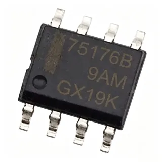
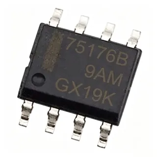
ESDA05CP - 5V Bi-Directional TVS/ESD Diode | MSKSEMI/Leiditech
Артикул: ESDA05CP ✓ Активен| Кол-во | Цена за ед. | Итого |
|---|---|---|
| 1 | $0.0274 | $0,03 |
| 10 | $0.022 | $0,22 |
| 100 | $0.0145 | $1,45 |
| 500 | $0.0098 | $4,90 |
| 1.000 | $0.0079 | $7,90 |
| 3.000 | $0.0067 | $20,10 |
ESDA05CP Обзор
A TVS (Transient Voltage Suppressor) diode is a clamping semiconductor device that diverts overvoltage transients away from sensitive circuitry by avalanche breakdown. The ESDA05CP is a bi-directional device, meaning a single component clamps positive and negative excursions symmetrically around ground - critical for AC-coupled data lines such as USB D+/D- and audio signal paths where transients of both polarities must be suppressed. The 5V working voltage matches common logic rails (USB VBUS, 3.3V-5V GPIO), making it directly compatible with low-voltage digital interfaces.
Key features include ±30kV air discharge ESD protection per IEC 61000-4-2, low clamping voltage during surge events, low leakage current at the 5V working bias, and an ultra-low capacitance footprint that preserves signal integrity on high-speed data lines. The DFN1006-2L package occupies less than 0.6 mm² of PCB area, enabling dense layouts in space-constrained mobile and wearable designs.
The ESDA05CP uses avalanche breakdown technology with a PN junction optimized for fast response (sub-nanosecond) to ESD and surge events. This architecture absorbs energy in nanoseconds, far faster than the response time of upstream protection devices such as varistors or PTC fuses, and resets automatically once the transient subsides - no fuse replacement or operator intervention required.
Typical applications include USB 2.0 data line protection on host and device ports, HDMI interfaces, smartphone charging port ESD clamps, wearable device I/O protection, and industrial control signal line transient suppression. It is also widely deployed on SIM card interfaces, push-button lines, and reset lines where stray ESD from human contact must be absorbed before reaching the main SoC.
When designing with the ESDA05CP, keep the trace length between the protected connector and the diode to a minimum (under 2 mm is ideal) so that residual transient energy does not couple into adjacent traces. Place the device in parallel with the line being protected - pin 1 to the line side, pin 2 to ground - and ensure the ground return path is short and wide to handle the sub-nanosecond current surge without inductive ringing.
Аналоги без доработки для ESDA05CP — тот же корпус, pin-to-pin совместимость. Компоненты в других корпусах, требующие переработки PCB, исключены.
Инструмент быстрого сравнения — выберите альтернативные компоненты для сравнения бок о бок:
ESDA05CP-ES
✅ Прямая замена📋 Справочный аналог (нет в каталоге)
ESDA05CP
✅ Прямая замена✓ В наличии
$0.0067 / шт.
Открыть даташит →PESD5V0L1BA
✅ Прямая замена📋 Справочный аналог (нет в каталоге)
ESD5V0S1B-N
✅ Прямая замена📋 Справочный аналог (нет в каталоге)
VESD05A1B-N
✅ Прямая замена📋 Справочный аналог (нет в каталоге)
CG0603LEU05BA
✅ Прямая замена📋 Справочный аналог (нет в каталоге)
ESDA05CP Максимальные параметры и электрические характеристики
| Device Type | Bi-directional TVS/ESD protection diode |
| Number of Lines | 1 |
| Working Voltage (Vrwm) | 5 V |
| Breakdown Voltage (Vbr) | 5.6 V (typical) |
| Peak Pulse Current (Ipp, 8/20us) | 8 A |
| Peak Pulse Power (Ppp, 8/20us) | 96 W |
| Диапазон рабочих температур | -55C to +125C |
| Корпус | DFN1006-2L (1.0 mm x 0.6 mm) |
| Тип монтажа | Surface Mount |
| Configuration | Bi-directional, single channel |
| Статус RoHS | Compliant |
Конфигурация выводов ESDA05CP
| Контакт 1 | Line — Protected signal line (anode/cathode - bi-directional, polarity does not matter) |
| Контакт 2 | GND — Ground return for clamped transient current |
Типичное применение
ESDA05CP подходит для 7 применениеs: USB 2.0 Data Line Protection, Smartphone USB-C Charging Port ESD Clamp, HDMI Display Interface Protection, Wearable Device I/O Protection, Industrial Control Signal Line Surge Protection, SIM Card and Push-Button Line Protection, Low-Speed GPIO and Reset Line Protection.
USB 2.0 Data Line Protection
The ESDA05CP is purpose-built for USB 2.0 data and power line ESD/surge protection, with a 5V working voltage that matches the USB VBUS rail directly. Its bi-directional design clamps both positive and negative transients on the D+ and D- data pair, while the DFN1006-2L 1.0 x 0.6 mm package fits inside any USB-A, USB-B, micro-USB, or USB-C connector footprint. The 96W peak pulse power (8/20us) easily absorbs cable-discharge events when users plug in charged cables - a frequent failure mode in unprotected designs. Place the device within 2 mm of the connector pins with a direct, wide ground return so the TVS shunt current returns to chassis ground before reaching the transceiver IC.
Рекомендуется
Smartphone USB-C Charging Port ESD Clamp
Inside a smartphone USB-C receptacle, board space is measured in tenths of a millimeter, and the ESDA05CP's DFN1006-2L (1.0 x 0.6 mm) package drops directly next to the high-speed lines. The 5V working voltage matches the VBUS pin of USB-C; the bi-directional configuration clamps the ±8kV contact / ±15kV air ESD strikes specified in IEC 61000-4-2 that occur during user handling. The sub-nanosecond response time prevents transient energy from reaching the main power-management IC or USB-PD controller. This part is widely second-sourced across MSKSEMI, Leiditech, and ElecSuper variants, enabling multi-vendor sourcing.
Рекомендуется
HDMI Display Interface Protection
HDMI TMDS lines carry high-speed differential data up to 6 Gbps that must be protected from ESD events during cable insertion. The ESDA05CP's 5V working voltage sits comfortably above the 3.3V HDMI signal swing, and its DFN1006-2L footprint allows a TVS to be placed on each TMDS pair near the HDMI connector. The low capacitance of a single-line DFN1006 TVS preserves signal integrity at HDMI 1.4b speeds, and the 8A peak pulse current absorbs cable-discharge events that would otherwise latch up the receiver. Stagger the placement of TVS arrays to balance layout symmetry and minimize intra-pair skew.
Рекомендуется
Wearable Device I/O Protection
Wearable devices - smartwatches, fitness bands, hearables - expose charging contacts and side buttons to constant human contact, creating frequent ESD strike opportunities. The ESDA05CP's DFN1006-2L package fits inside any wearable chassis where PCB real estate is below 4 mm². Place one ESDA05CP on each charging-pad input and one on each exposed GPIO push-button line to absorb hand-held electrostatic discharge events before they reach the SoC. The 5V working voltage is compatible with 5V charging-pad rails, and the bi-directional configuration handles both polarities common with inductive coupling through wearables.
Рекомендуется
Industrial Control Signal Line Surge Protection
Industrial control systems using 24V signal lines often run alongside power wiring in cable trays, exposing I/O to inductive surge events from motors, solenoids, and relay switching. The ESDA05CP, with its 5V working voltage and 8A peak pulse current, is ideal for low-voltage digital signal lines including 5V logic, RS-232 transceivers, and GPIO outputs from PLCs and motor controllers. The sub-nanosecond response time shuts down transients long before they can latch up the downstream logic IC, and the DFN1006-2L package allows dense placement on multi-channel I/O cards. For higher-voltage signal lines, select a TVS with Vrwm matching the system voltage.
Рекомендуется
SIM Card and Push-Button Line Protection
SIM card interfaces and user-accessible push-buttons are frequent ESD entry points in mobile phones, IoT gateways, and remote-control designs. The ESDA05CP's 5V working voltage matches both the SIM card supply and 5V-tolerant GPIO lines, and the 1.0 x 0.6 mm DFN1006-2L footprint fits within the SIM connector outline. A single ESDA05CP per SIM data line clamps ±15kV air discharge events per IEC 61000-4-2, and the sub-nanosecond response preserves SIM card data integrity during hand-handling transients. For multi-button matrices, scale to one ESDA05CP per exposed pin.
Рекомендуется
Low-Speed GPIO and Reset Line Protection
Any 5V GPIO line that is exposed to user contact or cable insertion deserves a TVS clamp to prevent latch-up of the downstream microcontroller. The ESDA05CP's 5V working voltage aligns with common 5V-tolerant MCU I/O, and the 96W peak pulse power easily absorbs IEC 61000-4-2 ESD gun test levels. Place one ESDA05CP on each exposed reset, interrupt, or mode-select line, with a low-inductance ground return to absorb transient current before it can develop into radiated EMI. This topology is standard practice in industrial HMI panels and consumer appliances with touch interfaces.
Рекомендуется
Сводка рекомендуемых товаров
Справочные инженерные данные для ESDA05CP — сравнение, рекомендации по проектированию и информация о соответствии.
Руководство по выбору
Сравнение с аналогами
| Параметр | Этот товар | ESDA05CP-ES | ESDA05CP (Leiditech) | PESD5V0L1BA | ESD5V0S1B-N | VESD05A1B-N |
|---|---|---|---|---|---|---|
| Brand | MSKSEMI | ElecSuper | Leiditech | NXP Semiconductors | onsemi | Vishay Intertechnology |
| Package | DFN1006-2L (1.0 x 0.6 mm) | DFN1006-2L - same | DFN1006-2L - same | DFN1006-2L - same | DFN1006-2L - same | DFN1006-2L - same |
| Working Voltage (Vrwm) | 5 V | 5 V | 5 V | 5 V | 5 V | 5 V |
| Configuration | Bi-directional, 1 line | Bi-directional, 1 line | Bi-directional, 1 line | Bi-directional, 1 line | Bi-directional, 1 line | Bi-directional, 1 line |
| Operating Temperature | -55C to +125C | -55C to +125C | -55C to +125C | -40C to +125C | -40C to +125C | -40C to +85C |
| RoHS Compliant | Yes | Yes | Yes | Yes | Yes | Yes |
Ключевые отличия
- Five-source drop-in availability (против PESD5V0L1BA (NXP))
- 96W peak pulse power in DFN1006-2L (против CG0603LEU05BA (Bourns))
- USB 2.0-specific design optimization (против ESD5V0S1B-N (onsemi))
Заметки по проектированию
Place the ESDA05CP within 2 mm of the connector pin being protected - longer trace inductance allows residual transient energy to develop voltage overshoot before reaching the TVS clamp. Use a wide, short ground return trace (or dedicated ground via) directly under pin 2 so the 8A peak pulse current returns to chassis ground without inducing ringing on adjacent signals. When protecting a differential pair (USB D+/D-, HDMI TMDS), keep the two TVS clamp traces equal length to avoid intra-pair skew.
For USB 2.0 (480 Mbps), the ESDA05CP's DFN1006-2L capacitance is acceptable on data lines. For USB 3.0 (5 Gbps) or higher, switch to a sub-0.5 pF TVS array such as the TPD6E004 or USBLC6 series - the ESDA05CP's capacitance would degrade the high-speed eye mask. Always run a signal-integrity simulation (eye diagram) before committing to a TVS on any interface above 1 Gbps.
Do not place the ESDA05CP on a high-impedance ground stub - inductive ringing during 8/20us surge events can double the effective clamping voltage. Always use a solid ground plane directly under the DFN1006 footprint. Also, do not connect the protected line directly through the TVS as a series element; the ESDA05CP must be in PARALLEL with the line, not in series, or the protected signal will be attenuated.
Estimated: At Vrwm = 5V with normal DC leakage (typically <1 uA), power dissipation is negligible and the DFN1006-2L thermal resistance (theta_JA ~ 500 C/W) is not a design concern. During an 8/20us surge event, the 96W peak pulse power is brief enough that thermal rise does not exceed junction limits; the device returns to ambient between events. Sustained DC overvoltage above breakdown, however, can cause thermal runaway - never operate the ESDA05CP continuously above Vbr.
Use standard DFN1006-2L land pattern with NSMD (non-solder mask defined) pads for best solder joint reliability. Recommended pad dimensions: 0.5 mm x 0.3 mm with 0.3 mm spacing - refer to IPC-7351 for the latest land-pattern calculator. The bottom thermal pad (if any) should be soldered to a copper pour of at least 1 mm² to provide mechanical and thermal anchoring during reflow.
Информация о соответствии
RoHS compliant per Jotrin product listing. REACH, halogen-free, and conflict-mineral status not explicitly stated in the provided verified data - confirm via manufacturer compliance declaration before EU-marked end-product certification. AEC-Q100 automotive qualification is not listed; for automotive designs, consider NXP's PESD5V0L1BA-Q (AEC-Q101) variant.