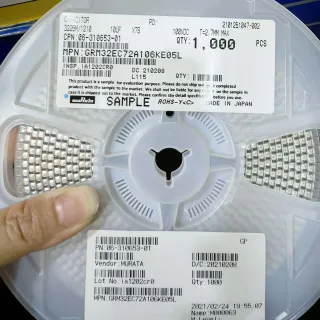
LXES03TAA1-199 - 1pF Bi-Dir ESD Diode 0201 | Murata | USB/HDMI
Артикул: LXES03TAA1-199 ✓ Активен| Кол-во | Цена за ед. | Итого |
|---|---|---|
| 1 | $0.11 | $0,11 |
| 10 | $0.07 | $0,70 |
| 100 | $0.04 | $4,00 |
| 500 | $0.029 | $14,50 |
| 1.000 | $0.022 | $22,00 |
| 10.000 | $0.017 | $170,00 |
LXES03TAA1-199 Обзор
A TVS diode is a specialized solid-state clamping device that diverts ESD and surge energy away from sensitive downstream ICs. In the protection hierarchy, TVS diodes sit at the connector-facing edge of a system, ahead of any series ferrite or common-mode choke and ahead of the PHY/MCU. The LXES family is specifically engineered for ultra-low parasitic capacitance to avoid attenuating or distorting high-frequency signals such as USB 2.0/3.x, HDMI, MIPI DSI/CSI-2, and antenna RF feeds. Bi-directional polarity allows placement across a differential pair or single-ended line without regard to DC bias direction.
Key features include a 30 kV contact-discharge rating per IEC 61000-4-2, an ultra-compact 0201 footprint (0.6 x 0.3 x 0.3 mm), and RoHS-compliant lead-free reflow profile compatibility. The package integrates two back-to-back steering diodes plus a TVS cell in a single die, minimizing loop inductance and maximizing clamping response time relative to discrete alternatives.
Architecturally, the LXES03TAA1-199 uses silicon avalanche technology, where the TVS junction breaks down at a controlled voltage (VBR) and shunts current to ground. The 1.0 pF typical capacitance is achieved through die geometry optimization and minimizes insertion-loss impact above 1 GHz. Source: Murata product data referenced on the official Murata EMEA product page (pim.murata.com / murata.com LXES T Series listing).
Typical applications include USB 2.0/3.0 high-speed data line protection, HDMI/MHL interface ESD clamps, smartphone antenna and SIM interfaces, wearable device charging ports, and IoT sensor data lines. Its miniature 0201 size makes it suitable for boards where PCB real estate is at a premium, such as mobile phones, TWS earbuds, AR/VR headsets, and compact sensor modules.
When designing in the LXES03TAA1-199, place it as close as possible to the connector with a short, wide ground return to the chassis or system ground. Avoid routing protected signal traces under the diode; the ungrounded paddle and pad geometry already provide adequate isolation but a clean ground via is essential. The 0201 size requires precise SMT stencil aperture control for reliable solder joint formation during reflow.
This page synthesizes Murata datasheet specifications, distributor pricing, and cross-reference drop-in alternatives for engineers evaluating the LXES03TAA1-199 in space-constrained, high-frequency interface designs.
Аналоги без доработки для LXES03TAA1-199 — тот же корпус, pin-to-pin совместимость. Компоненты в других корпусах, требующие переработки PCB, исключены.
Инструмент быстрого сравнения — выберите альтернативные компоненты для сравнения бок о бок:
LXES03TAA1-098
✅ Прямая замена📋 Справочный аналог (нет в каталоге)
LXES03TAA1-154
✅ Прямая замена📋 Справочный аналог (нет в каталоге)
LXES03TAA2-199
✅ Прямая замена📋 Справочный аналог (нет в каталоге)
RClamp0501P
✅ Прямая замена📋 Справочный аналог (нет в каталоге)
PRTR5V0U4D
✅ Прямая замена📋 Справочный аналог (нет в каталоге)
ESDA5-1BU
✅ Прямая замена📋 Справочный аналог (нет в каталоге)
LXES03TAA1-199 Максимальные параметры и электрические характеристики
| Part Number | LXES03TAA1-199 |
| Manufacturer | Murata Manufacturing |
| Device Type | Bi-directional TVS / ESD Protection Diode |
| Series | LXES T Series |
| Number of Channels | 1 channel |
| Package / Size | 0201 (0.6 x 0.3 mm) |
| Тип монтажа | Surface Mount |
| Capacitance (Typical) | 1.0 pF |
| Reverse Stand-off Voltage (Vrwm) | 5.5 V |
| Breakdown Voltage (VBR min) | 7.0 V |
| Peak Pulse Current (8/20 µs) | 1.5 A |
| ESD Rating (Contact, IEC 61000-4-2) | 30 kV |
| Polarity | Bi-directional |
| RoHS / Lead-Free | RoHS compliant, lead-free |
| Recommended Applications | Consumer equipment, automotive, industrial, medical |
Конфигурация выводов LXES03TAA1-199
| Контакт 1 | PAD1 — Signal / line connection (protected signal input) |
| Контакт 2 | PAD2 — Ground / return (connection to chassis or system ground) |
Типичное применение
LXES03TAA1-199 подходит для 6 применениеs: USB 3.0 / 3.1 High-Speed Data Line Protection, HDMI / MIPI DSI Display Interface Protection, Smartphone Antenna and SIM Interface Protection, Wearable Device Charging Port (TWS Earbuds / Smartwatch), IoT Sensor Module Data Line ESD Clamp, Automotive Infotainment / Camera Interface Protection.
USB 3.0 / 3.1 High-Speed Data Line Protection
The LXES03TAA1-199 protects SuperSpeed USB differential pairs (5 Gbps for USB 3.0 Gen 1, 10 Gbps for USB 3.1 Gen 2) and CC/SBU sideband lines from connector-level ESD events. Its 1.0 pF line capacitance keeps insertion loss below 1 dB at 5 GHz, preserving eye-diagram margin through the receptacle. The 30 kV IEC 61000-4-2 contact rating defends against direct human discharge to the USB-C tongue, while the 7 V breakdown sits above the CC logic swing of 3.3 V. Place at the connector, route the protected signal through to the PHY, and tie the ground pad with a short via to chassis ground. Compared to a 10 pF TVS, this Murata part does not require signal-compensation in the PHY redriver.
Рекомендуется
HDMI / MIPI DSI Display Interface Protection
For HDMI 1.4 (1.65 Gbps TMDS) up to HDMI 2.0 (6 Gbps) and MIPI DSI/CSI-2 camera serial interfaces, the LXES03TAA1-199 offers 1.0 pF capacitance that preserves signal rise time below 50 ps and prevents eye-pattern closing. The 1.5 A peak pulse current (8/20 µs) absorbs hot-plug surges that occur when consumer cables are inserted into powered displays. The 0201 footprint allows multiple clamps to fit in the tight space between an HDMI connector and the SoC display controller. The 5.5 V reverse stand-off voltage is well above the 3.3 V typical common-mode voltage of these interfaces, preventing false triggering during normal signal swing.
Рекомендуется
Smartphone Antenna and SIM Interface Protection
Inside a modern smartphone the antenna tuner, SIM socket, and NFC antenna loop all need ultra-low capacitance ESD protection. The LXES03TAA1-199 at 1.0 pF adds negligible parasitic to a 1.8 GHz or 2.4 GHz antenna matching network, preserving return loss below -15 dB. Its 0201 footprint allows protection at the very edge of the antenna feed where loop inductance is critical to clamping effectiveness. Bi-directional operation matches the symmetrical AC-coupled nature of NFC and main antenna lines. The 30 kV contact rating meets OEM smartphone reliability targets for direct discharge events during assembly or user handling.
Рекомендуется
Wearable Device Charging Port (TWS Earbuds / Smartwatch)
True-wireless earbuds and smartwatches have microscopic PCBs that demand the smallest possible ESD footprint. The LXES03TAA1-199 occupies only 0.18 mm² of board area, enabling a charging-pin ESD clamp next to the pogo-pin pads without crowding the battery management IC. The 1.5 A peak current (8/20 µs) handles the worst-case inductive kick observed when the charging cradle disconnects from a powered USB source. The 7 V VBR is set above the 5 V battery rail but well below the failure voltage of modern Li-ion charge controllers (typically 8-12 V abs max). With 1 pF capacitance, the clamp does not appear in the USB-PD CC pin signal path measurement budget.
Рекомендуется
IoT Sensor Module Data Line ESD Clamp
Industrial and consumer IoT sensor nodes (Zigbee, Bluetooth LE, LoRa, Wi-Fi) carry 2.4 GHz or sub-GHz RF signals that must survive field-deployment ESD events. The LXES03TAA1-199 protects SPI, UART, and antenna lines without measurably impacting link budget. The 5.5 V working voltage covers the 3.3 V logic levels common to Nordic, TI CC series, and Espressif modules. Its 0201 size preserves PCB space for antenna keep-out regions. The 30 kV contact ESD rating gives fielded IoT products survival against installer-arcing or static-prone environments.
Рекомендуется
Automotive Infotainment / Camera Interface Protection
In automotive infotainment and surround-view camera modules, the LXES03TAA1-199 protects FPD-Link III, GMSL, or standard LVDS serializer lines from assembly-line and in-service ESD. The bi-directional characteristic suits AC-coupled differential pairs common to automotive SerDes. The 7 V VBR is above the 3.3 V or 5 V supply rails but below the serializer absolute-maximum ratings. While the part itself is not AEC-Q100 qualified (the -199 suffix is a packaging option, not an automotive grade), its TVS architecture and silicon junction are well-characterized for automotive environments when procured in PPAP-level supply chains.
Рекомендуется
Сводка рекомендуемых товаров
Справочные инженерные данные для LXES03TAA1-199 — сравнение, рекомендации по проектированию и информация о соответствии.
Руководство по выбору
Сравнение с аналогами
| Параметр | Этот товар | LXES03TAA1-098 | LXES03TAA2-199 | RClamp0501P | PRTR5V0U4D | ESDA5-1BU |
|---|---|---|---|---|---|---|
| Brand | Murata Manufacturing | Murata Manufacturing | Murata Manufacturing | Semtech | NXP Semiconductors | STMicroelectronics |
| Package | 0201 (0.6 x 0.3 mm) | 0201 - same | 0201 - same | 0201 - same | 0201 - same | 0201 - same |
| Capacitance (Typical) | 1.0 pF | 1.0 pF | ~3 pF | 0.7 pF | 0.5 pF | 1.0 pF |
| Reverse Stand-off Voltage (Vrwm) | 5.5 V | 5.5 V | 5.5 V | 5.0 V | 5.0 V | 5.0 V |
| Breakdown Voltage (VBR min) | 7.0 V | 6.0 V (variant) | 7.0 V | 6.0 V | 6.0 V | 6.0 V |
| ESD Rating (IEC 61000-4-2 Contact) | 30 kV | 30 kV | 30 kV | 15 kV | 8 kV | 30 kV |
| Channels | 1 | 1 | 1 | 1 | 4 | 1 |
| Polarity | Bi-directional | Bi-directional | Bi-directional | Bi-directional | Bi-directional | Bi-directional |
| Peak Pulse Current (8/20 µs) | 1.5 A | 1.5 A | 1.0 A | 1.0 A | 0.5 A | 1.0 A |
Ключевые отличия
- Lowest typical capacitance in 0201 form factor with full 30 kV ESD rating (против RClamp0501P)
- Single-channel flexibility vs integrated quad-channel arrays (против PRTR5V0U4D)
- Murata T-Series one-stop option codes simplify inventory (против ESDA5-1BU)
Заметки по проектированию
Estimated: Mount the LXES03TAA1-199 within 2 mm of the connector shell or signal pad exit, with the ground pad tied through 2 parallel vias (each 0.25 mm drill) directly to the chassis ground pour. Total loop inductance from clamp to via should be <1 nH; longer traces degrade clamping effectiveness above 8 kV contact ESD.
Route the protected signal trace on the layer immediately below the 0201 pad; avoid vias in/out on the protected segment to keep parasitic stub inductance under 50 pH. Maintain a 0.2 mm keepout between the 0201 device pad edges and any adjacent copper to prevent solder-bridging during reflow (0201 stencil aperture: 0.25 mm x 0.40 mm).
Do not place the LXES03TAA1-199 in series with the signal (it is a shunt device across the line, not a series TVS). Verify the protected line impedance-whether single-ended 50 ohm SE or differential 90 ohm-after the clamp is added; the 1 pF capacitance adds roughly 30 mil of stub at 5 GHz equivalent which remains well below typical USB/HDMI limits but can be a concern on antenna feeds if not modeled.
Estimated: at 1 pF and 5 GHz the S21 insertion loss contributed by LXES03TAA1-199 is approximately -0.18 dB on 50 ohm SE. This is well within USB 3.x, HDMI 2.0, and PCIe Gen 3 compliance budgets. For MIPI D-PHY 2.5 GHz lanes expect <0.1 dB degradation. Beyond 10 GHz (USB 3.2 Gen 2x2 HDR), consider a 0.5 pF or smaller-clamp alternative such as RClamp0501P.
Информация о соответствии
RoHS and lead-free per Murata product page. Halogen-free status not explicitly stated in the source data-marked unknown. Part is not AEC-Q100 qualified in the -199 (commercial) option code; verify with Murata for automotive grade.