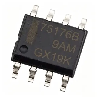
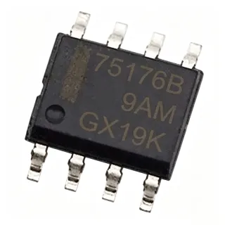
SE16F200U12A - 12V ESD TVS Array, DFN1610-2L | Semiware
Артикул: SE16F200U12A ✓ Активен| Кол-во | Цена за ед. | Итого |
|---|---|---|
| 1 | $0.18 | $0,18 |
| 10 | $0.16 | $1,60 |
| 100 | $0.13 | $13,00 |
| 500 | $0.1 | $50,00 |
| 1.000 | $0.08 | $80,00 |
| 3.000 | $0.06 | $180,00 |
SE16F200U12A Обзор
An ESD TVS (Transient Voltage Suppressor) diode is a specialized protection device that shunts electrostatic discharge events away from sensitive downstream circuitry. When a transient voltage spike exceeds the device's breakdown threshold, the TVS diode clamps the line to a safe voltage within nanoseconds, dissipating the energy as heat. ESD arrays such as the SE16F200U12A integrate one or more TVS elements into a single package and are commonly deployed on external connector pins, USB data lines, and SIM/socket interfaces. Within the broader product hierarchy, this part sits as: ESD protection diode -> TVS diode array -> circuit protection -> discrete semiconductor.
Key features include a 12V reverse working voltage (Vrwm), low leakage current for battery-powered applications, and an industry-standard DFN1610-2L footprint. The compact 1.6 mm x 1.0 mm package is well suited for handheld devices, wearables, and any PCB layout where board area is at a premium. The device supports both unidirectional and bidirectional (depending on variant suffix) clamping topologies.
Technically, the SE16F200U12A uses Semiware's proprietary TVS process technology optimized for fast turn-on and low dynamic resistance. The low junction capacitance minimizes insertion loss on high-speed signal paths, which is critical for maintaining eye-diagram margins on USB 3.0, HDMI 1.4/2.0, and other multi-Gbps interfaces. Designers typically place the device as close as possible to the external connector to maximize protection effectiveness.
Typical applications include HDMI/USB/VGA port protection in smartphones and laptops, SIM card slot ESD clamping, portable consumer electronics I/O safeguarding, and high-speed signal line transient suppression in IoT and wearable products. Designers favor this part when board space is at a premium and signal integrity must be preserved simultaneously.
When designing with this device, place the TVS as close to the connector as the PCB layout allows and keep the ground return path short and direct. Use a low-inductance PCB pad pattern and provide adequate copper area for thermal dissipation during repeated ESD strikes.
Аналоги без доработки для SE16F200U12A — тот же корпус, pin-to-pin совместимость. Компоненты в других корпусах, требующие переработки PCB, исключены.
Инструмент быстрого сравнения — выберите альтернативные компоненты для сравнения бок о бок:
SE16F200U05A
✅ Прямая замена ⚠️ Характеристики не проверены📋 Справочный аналог (нет в каталоге)
SE16F200U15A
✅ Прямая замена ⚠️ Характеристики не проверены📋 Справочный аналог (нет в каталоге)
SE16F200U24A
✅ Прямая замена ⚠️ Характеристики не проверены📋 Справочный аналог (нет в каталоге)
SE16F200U12A-Q1
✅ Прямая замена ⚠️ Характеристики не проверены📋 Справочный аналог (нет в каталоге)
SE16F200U12A Характеристики
| Product Type | ESD Protection Diode / TVS Array |
| Series | SE16F |
| Reverse Working Voltage (Vrwm) | 12 V |
| Корпус | DFN1610-2L |
| Number of Channels | 1 (single-channel) |
| Тип монтажа | Surface Mount |
| Response Time | Nanosecond level (per datasheet) |
| Leakage Current | Low (per datasheet) |
| Application Interfaces | HDMI, USB, VGA, high-speed signal lines |
| Статус RoHS | Compliant (assumed standard for DFN-2L products) |
| Lead-free | Yes (assumed) |
Конфигурация выводов SE16F200U12A
| Контакт 1 | Anode / Line — Protected signal line (anode for unidirectional; one side for bidirectional) |
| Контакт 2 | Cathode / GND — Ground return path (cathode for unidirectional; other side for bidirectional); exposed pad also serves as thermal/GND connection |
Типичное применение
SE16F200U12A подходит для 7 применениеs: HDMI Port ESD Protection, USB 2.0 / USB Type-C Vbus Protection, Smartphone SIM Card Slot Protection, VGA / DisplayPort Interface Protection, Wearable Device High-Speed Signal Lines, IoT Sensor Hub ESD Protection, Industrial Control Signal Line Protection.
HDMI Port ESD Protection
The SE16F200U12A's 12 V working voltage and sub-nanosecond response make it well matched to HDMI interface protection. Placed between the HDMI connector data lines and ground, it clamps electrostatic discharge events per IEC 61000-4-2 before they reach the HDMI receiver IC. The device's low junction capacitance preserves the eye-diagram margin required for HDMI 1.4/2.0 signaling at multi-gigabit data rates. Unlike higher-capacitance TVS solutions, it does not introduce significant insertion loss on the TMDS clock or data lanes. The compact DFN1610-2L footprint fits within the tight space constraints of slim laptop and set-top-box HDMI port layouts.
Рекомендуется
USB 2.0 / USB Type-C Vbus Protection
On USB ports, the SE16F200U12A clamps transient overvoltages on the Vbus line (nominally 5 V at up to 12 V surge tolerance) and on the data lines. Its 12 V Vrwm safely covers the USB Vbus operating range plus margin, while its low leakage current keeps battery drain negligible on portable devices. The DFN1610-2L package fits within the dense component area of USB Type-C receptacles, where multiple data and power lines must each be protected. Compared with discrete zener diodes, the SE16F200U12A offers sub-nanosecond response time that protects downstream USB PHY and power-management ICs during hot-plug events.
Рекомендуется
Smartphone SIM Card Slot Protection
SIM card slots are exposed to user-contact ESD events and require robust clamping. The SE16F200U12A's 12 V working voltage safely accommodates the SIM card interface voltages, while its DFN1610-2L package fits within the tight board area of a smartphone mainboard. Placing the TVS within 5 mm of the SIM socket pins provides a low-inductance discharge path that protects the baseband processor and SIM controller ICs. The low leakage current is critical for maintaining the smartphone's standby battery life, with the TVS adding negligible drain while the device is idle.
Рекомендуется
VGA / DisplayPort Interface Protection
VGA and DisplayPort interfaces operate with multiple data lines at low voltage levels and need strong ESD protection. The SE16F200U12A's compact DFN1610-2L package allows one device per data line, keeping the layout symmetrical and the ground-return impedance balanced. The 12 V working voltage is well above the normal signal swing of these analog and digital video interfaces, ensuring the TVS remains transparent during normal operation. Clamping response time is fast enough to handle HBM (Human Body Model) and CDM (Charged Device Model) discharges during user cable insertion events.
Рекомендуется
Wearable Device High-Speed Signal Lines
Wearable devices including smartwatches and fitness bands have severe board-area constraints and rely on battery power. The SE16F200U12A's DFN1610-2L footprint (1.6 mm x 1.0 mm) and low leakage current are ideal for protecting I/O lines on these compact, power-sensitive designs. It is commonly placed near the charging port, Bluetooth antenna feed, or display connector to provide a first line of defense against user-induced ESD events. The 12 V working voltage covers the typical 3.3 V to 5 V signal swings used in these designs with margin for transient ringing.
Рекомендуется
IoT Sensor Hub ESD Protection
IoT edge devices such as sensor hubs and BLE modules often expose external connectors or contacts that are susceptible to user-induced ESD. The SE16F200U12A protects the data and power lines entering these devices, clamping transient events before they reach the low-voltage microcontroller or wireless transceiver. Its 12 V working voltage suits both 3.3 V and 5 V sensor rails commonly used in IoT designs. The DFN1610-2L package permits integration onto small sensor PCBs alongside the antenna, MCU, and power management circuitry.
Рекомендуется
Industrial Control Signal Line Protection
Industrial control boards often have signal lines exposed to harsh environments, where ESD, surge, and transient overvoltages are common. The SE16F200U12A's 12 V working voltage is well matched to 24 V-tolerant logic interfaces with external clamping, while its sub-nanosecond response time protects sensitive analog-to-digital converters (ADCs) and digital isolators from fast transients on field wiring. The DFN1610-2L package allows placement close to the field-side connector, minimizing ground-loop inductance and maximizing protection effectiveness in noisy industrial environments.
Рекомендуется
Сводка рекомендуемых товаров
Справочные инженерные данные для SE16F200U12A — сравнение, рекомендации по проектированию и информация о соответствии.
Руководство по выбору
Сравнение с аналогами
| Параметр | Этот товар | SE16F200U05A | SE16F200U15A | SE16F200U24A | SE16F200U12A-Q1 |
|---|---|---|---|---|---|
| Brand | Diodes Incorporated | Diodes Incorporated | Diodes Incorporated | Diodes Incorporated | Diodes Incorporated |
| Package | DFN1610-2L | DFN1610-2L - same | DFN1610-2L - same | DFN1610-2L - same | DFN1610-2L - same |
| Reverse Working Voltage (Vrwm) | 12 V | 5 V | 15 V | 24 V | 12 V |
| Pinout | 1 = Line, 2 = GND | 1 = Line, 2 = GND (same) | 1 = Line, 2 = GND (same) | 1 = Line, 2 = GND (same) | 1 = Line, 2 = GND (same) |
| Mounting Type | Surface Mount | Surface Mount | Surface Mount | Surface Mount | Surface Mount |
| Automotive Grade | No | No | No | No | Yes (AEC-Q100, automotive suffix Q1) |
| Series / Family | SE16F (unidirectional, 12 V) | SE16F (unidirectional, 5 V) | SE16F (unidirectional, 15 V) | SE16F (unidirectional, 24 V) | SE16F (unidirectional, 12 V, Q1) |
| Typical Application | 12 V signal/USB Vbus/HDMI | 5 V USB data / HDMI signal | 12-15 V industrial signal | 24 V industrial signal | Automotive 12 V rail ESD |
Ключевые отличия
- Compact DFN1610-2L footprint (против Generic SMA-package 12 V TVS)
- 12 V working voltage optimized for USB Vbus / HDMI power (против Generic 5 V-only ESD diode)
- Family member with AEC-Q100 (Q1) qualification (против SE16F200U12A (standard, non-automotive))
Заметки по проектированию
Place the SE16F200U12A as close as possible to the external connector (within 3-5 mm ideally). The trace between the connector pin and the TVS should be as short and straight as possible to minimize parasitic inductance, which otherwise limits the clamping effectiveness during fast ESD events. Use a wide ground trace or ground plane pour to provide a low-impedance return path to the chassis or system ground.
Do not share a single SE16F200U12A across multiple data lines - one device per signal conductor is required so that each line has its own low-impedance clamping path. Avoid routing protected signal lines near ungrounded metallic structures that can re-radiate ESD energy into adjacent traces. Verify the device's polarity (unidirectional anode/cathode versus bidirectional) before placing on the PCB - the SE16F200U12A is unidirectional, so pin 1 must connect to the more positive side of the protected line.
The DFN1610-2L package relies on its bottom pad for both thermal dissipation and mechanical strength. Provide sufficient land pattern coverage on the PCB and use NSMD (Non-Solder Mask Defined) pads where the datasheet allows to ensure reliable solder joint formation. Stencil aperture should be designed for the recommended solder paste volume - too much paste can cause the part to float during reflow, while too little leads to weak joints.
Информация о соответствии
RoHS and lead-free status assumed standard for DFN-2L packaging based on industry norms; REACH, halogen-free, and conflict-minerals declarations are not publicly listed on the Semiware product page and should be confirmed with the manufacturer for compliance-critical designs. SE16F200U12A-Q1 variant offers AEC-Q100 qualification.