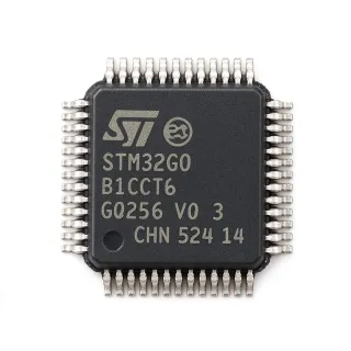
LPC2131FBD64 - 60MHz ARM7 MCU, 32KB Flash | NXP
MPN: LPC2131FBD64 ✗ Tapus ng BuhayLPC2131FBD64 Ulas
An ARM7TDMI-S microcontroller is a 32-bit RISC device that combines a conventional processor core, embedded program memory, and dedicated peripherals in one integrated circuit. Its position in the product hierarchy is microcontroller, then 32-bit RISC microcontroller, then ARM7TDMI-S embedded controller. The architecture supports 32-bit code execution while retaining deterministic interrupt-driven operation for real-time control workloads.
Principal features include a 60 MHz maximum clock, 32 KB of embedded high-speed flash, 8 KB of SRAM, a 10-bit ADC, an on-chip DAC, PWM outputs, and multiple GPIO. The 128-bit memory interface and accelerator architecture improve instruction throughput. In-System Programming and In-Application Programming support add manufacturing and field-update flexibility without removing the microcontroller from its target circuit.
The LPC2131/32/34/36/38 family uses a common hardware platform across several flash configurations. The 32 KB version has lower on-chip memory than the 64, 128, 256, and 512 KB family members, but retains the same 60 MHz ARM7TDMI-S core and 64-pin LQFP footprint. This makes the LPC2131FBD64 appropriate for compact code where external memory would otherwise increase cost and board area.
Typical applications include industrial data loggers, serial protocol converters, motor and process controllers, test equipment, and communications gateways. Its mixed-signal peripherals allow an analog sensor interface and digital control logic to share one device, while PWM and capture functions support actuator monitoring and timing tasks.
When designing around the LPC2131FBD64, check every peripheral pin against the selected board variant and provide the decoupling and oscillator arrangements shown in the manufacturer datasheet. Because this is an established ARM7 design, confirm that current toolchain, library, and driver support covers the exact firmware and production requirements before committing to a new design.
This page consolidates core specifications, ordering variants, comparison data, and practical design guidance. It also documents where package-level verification and datasheet pin descriptions should be used, helping engineers evaluate the LPC2131FBD64 without relying on generic microcontroller recommendations.
Mga alternatibo na pwedeng ilagay na LPC2131FBD64 — parehas na package, pin-to-pin na katugmang. Hindi kasama ang mga bahagi ng iba't-ibang package na nangangailangan ng pagpapaayos ng PCB.
Variante sa Seri na ito
Katulad na modelo sa serye na katugma sa pagpasok LPC2131FBD64 (parehas na form factor at footprint) — pagkakaiba sa ADC Resolution, Package, Product Type, Supply Voltage.
LPC2131FBD64/01
✅ Drop-InMagkontak para sa presyo
Tingnan ang Datasheet →LPC2131FBD64/01,15
✅ Drop-In📋 Alternatibo na Reference (hindi sa katalogo)
LPC2131FBD64/01,11
✅ Drop-In📋 Alternatibo na Reference (hindi sa katalogo)
LPC2131FBD64/01S
✅ Drop-In📋 Alternatibo na Reference (hindi sa katalogo)
LPC2131FBD64 Mga Pinakamataas na Rating at Electrical Characteristics
| Product Type | 16/32-bit ARM7TDMI-S RISC microcontroller |
| Maximum CPU Clock | 60 MHz |
| Embedded Flash Memory | 32 KB |
| Flash Organization | 32K x 8 bits |
| SRAM | 8 KB |
| ADC Resolution | 10 bits |
| DAC | Integrated |
| Volte ng Pagbibigay | 3.3 V |
| Processor Core | ARM7TDMI-S |
| Memory Interface | 128 bits wide |
| Program Memory | 32 KB embedded high-speed flash |
| Programming Support | ISP and IAP |
| Packhaging | 64-pin LQFP, 10 x 10 mm |
| Uri ng Pagpapasok | Surface mount |
| Tindminan RoHS | unknown |
| REACH Status | unknown |
Gabay sa Pin Configuration ng LPC2131FBD64 64-pin lqfp, 10 x 10 mm
Pin configuration para sa LPC2131FBD64 (64-pin lqfp, 10 x 10 mm package). Kasama sa digital IC na ito ang GPIO, mga communication interface (UART, SPI, I2C), at mga power pin. Sumangguni sa datasheet ng manufacturer para sa mga alternatibong function ng pin at mga opsyon sa configuration. Mahalaga para sa disenyo ng embedded system at PCB layout.

Wala ng detalyadong pinout data na magagamit para sa LPC2131FBD64.
Sumangguni sa datasheet para sa buong pin configuration.
Tipikal na mga Gamit
LPC2131FBD64 ay nararapat para sa 6 aplikasyons: Industrial Data Acquisition Controller, Serial Protocol Converter, Motor and Process Control, Communications Gateway Module, Embedded Test and Measurement, Legacy ARM7 Equipment Upgrade.
Industrial Data Acquisition Controller
The LPC2131FBD64 fits compact data-acquisition and condition-monitoring equipment because its 60 MHz ARM7TDMI-S core can service interrupt-driven sampling while the integrated 10-bit ADC handles analog sensor inputs. Its 32 KB flash and 8 KB of SRAM are sufficient for compact buffering, calibration tables, and communication routines. Use the PWM outputs for excitation or reference timing, and verify the analog pin multiplexing against the NXP datasheet before final routing.
Inirekomenda
Serial Protocol Converter
The LPC2131FBD64 can serve as a protocol-conversion gateway between legacy serial equipment and a host controller. The ARM7TDMI-S core executes at 60 MHz, allowing the firmware to handle framing, checksums, buffering, and real-time event scheduling, while the 32 KB flash footprint stores fixed protocol tables and 8 KB of SRAM supports short frame buffering. Its integrated ADC and DAC are optional if the converter also performs analog monitoring.
Inirekomenda
Motor and Process Control
The LPC2131FBD64 is appropriate for small motor controllers and industrial process-control modules where deterministic timing, mixed-signal I/O, and compact firmware are priorities. Its 60 MHz core supports rapid control-loop execution, the PWM channels can generate actuator commands, and the 10-bit ADC supports feedback measurement. Keep the analog reference, power routing, and PWM outputs within the electrical conditions defined in the manufacturer datasheet.
Inirekomenda
Communications Gateway Module
The LPC2131FBD64 can form the control core of a small communications gateway that supervises UART, SPI, and other embedded interfaces. Its 128-bit memory interface and accelerator architecture support efficient 32-bit instruction execution at the 60 MHz clock, while ISP and IAP simplify production programming and controlled firmware updates. The 32 KB flash budget is suitable for lightweight protocol stacks, not large TCP or TLS implementations.
Inirekomenda
Embedded Test and Measurement
The LPC2131FBD64 is useful in legacy-compatible test equipment where stimulus generation, timing, and data capture must share one microcontroller. Its PWM blocks, ADC, DAC, GPIO, and 60 MHz processing core support measurement sequencing and response generation within a single controller. The 8 KB of SRAM limits long waveform capture, so use external storage when records exceed the device’s local buffering capacity.
Inirekomenda
Legacy ARM7 Equipment Upgrade
The LPC2131FBD64 is appropriate for maintaining or selectively upgrading established ARM7TDMI-S equipment without introducing a new processor architecture or board form factor. The familiar 64-LQFP footprint, 60 MHz clock, and 32 KB flash organization allow an existing design to retain much of its software and hardware structure. Confirm pin multiplexing, peripheral assignments, and application-code compatibility before treating the upgrade as a component substitution.
Inirekomenda
Buod ng mga Inirekomendang Produkto
Impormasyon ng Talumpati sa Engineering for LPC2131FBD64 — ikabit, gabay sa disenyo, at impormasyon ng pagsunod sa kautusan.
Paunawang Hanapin
Ikabit sa Mga Alternatibo
| Parametro | Ito ang Producto | LPC2131FBD64/01 | LPC2131FBD64/01,15 | LPC2131FBD64/01,11 | LPC2131FBD64/01S |
|---|---|---|---|---|---|
| Brand | NXP Semiconductors | NXP Semiconductors | NXP Semiconductors | NXP Semiconductors | NXP Semiconductors |
| Package | 64-LQFP (10 x 10 mm) | 64-LQFP (10 x 10 mm) - same | 64-LQFP (10 x 10 mm) - same | 64-LQFP (10 x 10 mm) - same | 64-LQFP (10 x 10 mm) - same |
| Processor Core | ARM7TDMI-S | ARM7TDMI-S | ARM7TDMI-S | ARM7TDMI-S | ARM7TDMI-S |
| Maximum CPU Clock | 60 MHz | 60 MHz | 60 MHz | 60 MHz | 60 MHz |
| Embedded Flash Memory | 32 KB | 32 KB | 32 KB | 32 KB | 32 KB |
| SRAM | 8 KB | 8 KB | 8 KB | 8 KB | 8 KB |
| ADC Resolution | 10 bits | 10 bits | 10 bits | 10 bits | 10 bits |
| Programming Support | ISP and IAP | ISP and IAP | ISP and IAP | ISP and IAP | ISP and IAP |
| Supply Voltage | 3.3 V | 3.3 V | 3.3 V | 3.3 V | 3.3 V |
Pangunahing mga Pagkakaiba
- Identical core and memory organization across documented ordering variants (kumpara saLPC2131FBD64/01,15)
- Mixed-signal integration reduces external component count (kumpara saLPC2131FBD64/01,11)
- Field-update capability within a constrained embedded footprint (kumpara saLPC2131FBD64/01S)
Talaan ng Disenyo
Route the 64-pin LQFP footprint in accordance with the NXP package drawing, including correct pad length, pitch, and exposed thermal considerations where applicable. Keep the 3.3 V supply pins and decoupling capacitors close to their assigned pins, and preserve the datasheet-recommended return path. Verify every multiplexed GPIO, ADC, DAC, PWM, and debug signal against the selected pin-connectivity table before releasing artwork.
Calculate the digital and analog load before fixing power capacity, then follow the manufacturer’s recommended supply voltage and decoupling arrangement. The ADC and DAC may require filtered analog references and separate routing to reduce coupling from switching nodes. For mixed-signal boards, partition analog and digital return paths carefully and avoid routing PWM edges beneath sensitive analog inputs.
Do not treat a 64-lead Cortex-M device as a pin-compatible substitute for this ARM7TDMI-S part. Confirm the complete pin-connectivity table, startup sequence, peripheral register map, and application code against the NXP family datasheet. Also verify that 32 KB of flash and 8 KB of SRAM are sufficient after linker-map analysis, including space reserved for bootloader, interrupt vectors, and IAP code.
Use the fastest available debug and serial programming interface only after confirming its pin multiplexing and signal-integrity requirements. Avoid long unterminated traces from the microcontroller to external connectors, especially on lines shared with ADC inputs. For PWM-driven loads, keep switching-current paths compact and provide local bulk decoupling so control-loop timing is not disturbed by supply transients.
Impormasyon ng Pagsunod sa Kautusan
Compliance attributes are not stated in the product documentation pages for this legacy device. Request current RoHS, REACH, and material-declaration documentation through the Request a Quote form on this page.