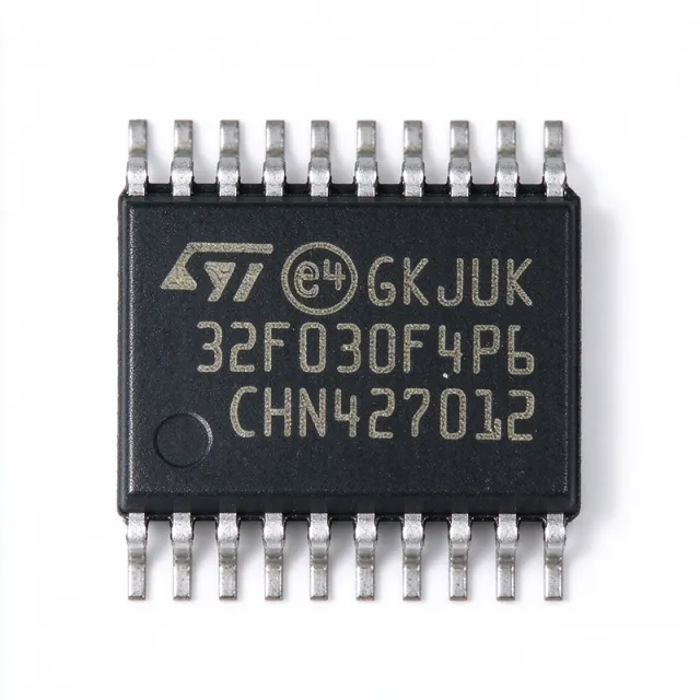
What is the STM32F030F4P6TR?
The STM32F030F4P6TR is an STMicroelectronics value-line, 32-bit Arm Cortex-M0 RISC microcontroller rated for operation up to 48 MHz. It provides 16 KB Flash organized as 16K x 8, 4 KB SRAM, ADC capability identified as 12-bit and 15-bit, timers, communication interfaces, and enhanced I/O resources. Its 2.4 V to 3.6 V operating range and 20-pin TSSOP package suit compact embedded-control, industrial automation, IoT, metering, and motor-control designs. The XAIPART database lists the lifecycle status as active, stock at 82,000 units, and an MOQ of 1 unit. Database pricing starts at $0.6469 for quantities of one and falls to $0.3773 at 1,000 units, as of 2026-11-01. Review the STM32F030F4P6TR product page for current procurement details.
This device sits at the compact end of the STM32F0 value-line family. The STM32F030x4, STM32F030x6, STM32F030x8, and STM32F030xC datasheet family covers multiple memory-density configurations, but the STM32F030F4P6TR itself is identified with 16 KB Flash and 4 KB SRAM. That combination supports small firmware images, short working buffers, sequencing logic, analog monitoring, and communication tasks without requiring a larger memory footprint.
Action: Select the STM32F030F4P6TR when a design fits a 48 MHz Cortex-M0 core, 16 KB Flash, 4 KB SRAM, a 2.4 V to 3.6 V supply, and the 20-pin TSSOP footprint. Move to another MCU if the application needs more memory, broader verified peripheral support, or a fully confirmed second-source pin-to-pin replacement.
How do you select and design in the STM32F030F4P6TR?
Begin with the application boundary. The verified data supports compact control systems that sample analog inputs, run timers, manage digital I/O, and use communication interfaces. It does not provide a complete pin table or every electrical limit, so use the official STMicroelectronics datasheet to confirm pin functions, alternate functions, absolute maximum ratings, clock requirements, and ADC channel details before committing a schematic or PCB.
Which verified specifications drive component selection?
| Selection parameter | Verified STM32F030F4P6TR value | Engineering implication |
|---|---|---|
| Processor core | Arm Cortex-M0 32-bit RISC | Provides a 32-bit embedded-processing platform for compact control logic. |
| Maximum CPU frequency | 48 MHz | Supports small control loops and auxiliary processing. |
| Flash memory | 16 KB, organized as 16K x 8 | Constrains firmware, libraries, and stored data to a compact footprint. |
| SRAM | 4 KB | Limits simultaneously resident working memory and buffer sizes. |
| Operating voltage | 2.4 V to 3.6 V | Defines the allowable MCU supply range and connected peripheral arrangement. |
| ADC capability | 12-bit and 15-bit | Supports measurement-oriented designs; channel mapping and sampling details require datasheet confirmation. |
| Package | 20-pin TSSOP, surface mount | Supports compact boards but requires deliberate escape routing and assembly planning. |
| Reset resources | POR and PDR | Provides verified power-on and power-down reset functionality. |
The memory budget deserves attention before firmware architecture is fixed. A 16 KB Flash target leaves limited room for a runtime, communication stack, application code, calibration data, and future revisions. The 4 KB SRAM figure likewise requires explicit buffer planning rather than assuming resources from a larger STM32 design. Use the MCU for state machines, acquisition sequencing, basic filtering, and supervisory logic when those functions fit the available space.
How should the supply voltage be planned?
Design the MCU rail around the verified 2.4 V minimum and 3.6 V maximum. The arithmetic span between those limits is 1.2 V. The power architecture must keep the MCU and connected peripherals within their own verified limits; the supplied data does not provide current consumption, regulator accuracy, or power-supply noise specifications. Confirm those details in the manufacturer documentation rather than treating the operating-voltage range as a complete power specification.
POR and PDR functionality is identified in the verified data. Designers should still verify reset behavior, external component requirements, and board-level power sequencing against the datasheet. No numerical bypass-capacitor recommendation is included in the supplied data, so this guide does not invent one.
How should ADC-based designs use the MCU?
The verified ADC capability of 12-bit and 15-bit makes the device relevant to digital meters, sensor nodes, and analog-feedback monitoring. A typical design can acquire a sensor signal, scale and calibrate the result, apply control logic, and present data through a serial interface or display. The external analog front end, reference arrangement, layout, and calibration strategy determine the measurement result; the MCU specification alone does not guarantee system accuracy.
Before selecting the part for a measurement design, verify ADC input count, channel mapping, reference behavior, sampling characteristics, and pin assignments in the datasheet. Also confirm whether the required signal and interface resources are simultaneously available. This avoids designing around the stated ADC resolution while overlooking a package or peripheral-resource constraint.
How do timers and communication interfaces affect architecture?
Timers, communication interfaces, and enhanced I/O resources are verified peripheral categories for this device. They support application patterns such as periodic sampling, relay or actuator sequencing, digital input management, serial data transfer, and simple motor-control interfaces. The supplied data does not enumerate timer channels, communication protocol variants, GPIO counts, interrupt mappings, or alternate-function assignments. Those details determine which functions can coexist on the 20-pin package.
For a motor-control interface, use timers and GPIO outputs for control signals and ADC capability for applicable analog feedback. Validate timer mapping, output frequency, pin alternate functions, and firmware timing against the device documentation. For an IoT node, treat the MCU as the local control processor and use a serial communications peripheral for data transfer. Confirm the required interface and low-power behavior before choosing the architecture.
What should PCB and assembly planning include?
The 20-pin TSSOP is surface mount and supports compact layouts, but the package still demands careful escape routing and adequate assembly clearance. The verified record does not include body dimensions, lead pitch, thermal data, or a recommended land pattern, so use the package drawing in the official datasheet. Preserve access to required programming, reset, clock, and communication signals without assuming that every adjacent pin can carry the same peripheral function.
The footprint, pin arrangement, voltage range, memory configuration, and relevant peripheral functions must all be considered when testing a replacement. The XAIPART component catalog can help locate alternatives, but compatibility still requires board-level and firmware validation.
How should procurement quantities be set?
The verified quantity tiers provide a clear basis for cost comparison as of 2026-11-01:
| Quantity | Database unit price | Pricing date |
|---|---|---|
| 1 or more | $0.6469 | As of 2026-11-01 |
| 10 or more | $0.4672 | As of 2026-11-01 |
| 100 or more | $0.4133 | As of 2026-11-01 |
| 500 or more | $0.3953 | As of 2026-11-01 |
| 1,000 or more | $0.3773 | As of 2026-11-01 |
The database also identifies $0.3773 as the base price as of 2026-11-01, matching the 1,000-unit tier. The difference between the one-unit price and the 1,000-unit price is $0.2696 per unit. These are database values with an as-of date, not permanent quotations; confirm current inventory, shipping, and commercial terms before releasing a production BOM.
Action: Build the design around a 2.4 V to 3.6 V rail, verify every required pin and peripheral against the datasheet, size firmware and SRAM explicitly, and use the dated quantity tiers—not a single spot price—for sourcing decisions.
Which alternatives are viable, and what requires validation?
The only supplied alternative is the HK32F030F4P6. The verified data identifies it as a package- and pinout-compatible engineering-review candidate, not as a fully qualified drop-in replacement. No verified memory or frequency difference is provided. It therefore requires firmware and peripheral-behavior validation before a production substitution.
| Comparison parameter | STM32F030F4P6TR | HK32F030F4P6 |
|---|---|---|
| Manufacturer | STMicroelectronics | HK32F030F4P6 |
| Package and pinout status | 20-pin TSSOP | Package- and pinout-compatible engineering-review candidate |
| Maximum CPU frequency | 48 MHz | No verified memory or frequency difference provided |
| Flash memory | 16 KB, organized as 16K x 8 | No verified memory or frequency difference provided |
| SRAM | 4 KB | No verified memory or frequency difference provided |
| Firmware and peripheral behavior | Arm Cortex-M0 32-bit RISC device | Requires validation |
| Replacement status | Reference component | Engineering review required before production use |
Package compatibility is necessary for board-level substitution, but it does not establish software compatibility. Firmware may depend on register definitions, peripheral behavior, interrupt layouts, clock configuration, startup routines, and device-specific libraries. The supplied data does not establish equivalence for those functions, so engineers should not treat the HK32F030F4P6 as an automatic substitution merely because its package and pinout are described as compatible.
Use a staged review for any second source. First compare the manufacturer documentation for pin functions, electrical limits, memory organization, clocking, and reset behavior. Then port the firmware and test the actual board, including ADC measurements, timer outputs, communication traffic, and reset behavior. The verified record does not support a broader list of drop-in alternatives, so adding an unverified part to the comparison would create sourcing risk rather than useful guidance.
Action: Treat the HK32F030F4P6 as a qualified engineering-review path, not a guaranteed drop-in part, and require firmware, electrical, and board-level validation before approving a production change.
What does the available lifecycle and supply data show?
The STM32F030F4P6TR has a verified lifecycle status of active, which supports continued design-in rather than positioning the record as an obsolete or discontinued component. The database reports 82,000 units of stock and an MOQ of 1 unit. Those figures describe the available record and do not guarantee future allocation or region-specific delivery.
| Supply indicator | Verified value | Procurement interpretation |
|---|---|---|
| Lifecycle status | Active | The component remains designated for current design activity. |
| Stock | 82,000 units | The database currently lists a substantial available quantity. |
| Minimum order quantity | 1 unit | Prototype and low-volume orders can begin below typical production quantities. |
| Lowest verified tier | $0.3773 at 1,000 units, as of 2026-11-01 | Use the dated tier when evaluating volume cost. |
Market positioning follows directly from the verified product classification. This is a value-line, 20-pin Cortex-M0 MCU intended for compact embedded-control roles, including industrial control, IoT, metering, and motor-control applications. It does not present itself as a high-bandwidth or large-memory platform. Its market fit therefore depends on whether the application can fit within 16 KB Flash and 4 KB SRAM while using the available timers, ADC capability, communication interfaces, and I/O resources.
For planned production builds, preserve the exact manufacturer part number and tape-and-reel ordering designation. Confirm current stock, quantity breaks, and shipment dates during purchasing. A broad stock figure should not replace a company-specific supply review for a scheduled build.
Action: Use the active lifecycle status and listed stock as positive sourcing evidence, but recheck availability and schedule a second-source review before committing a high-volume or long-lived product.
What trends should buyers monitor for this MCU?
The most important trend to monitor is fit between rising firmware complexity and a deliberately small memory footprint. The verified 16 KB Flash and 4 KB SRAM configuration creates a clear design boundary. As control products add communications, calibration, diagnostics, and field-upgrade functions, engineers should compare the complete firmware estimate against Flash and the peak working-set estimate against SRAM. A faster clock cannot compensate for insufficient memory, so resource planning should precede any assumption that additional code will fit.
Second, monitor how analog requirements affect board partitioning. The verified 12-bit and 15-bit ADC capability supports metering and sensor-node use cases, but the external front end and reference design remain part of the measurement solution. A product that adds more analog channels, higher accuracy, or stricter calibration requirements may require a different MCU even when the original STM32F030F4P6TR remains electrically suitable.
Third, watch supply strategy as firmware support matures. The active status, 82,000-unit stock record, MOQ of 1, and five verified price tiers support both prototyping and planned volume purchasing. At the same time, the dated pricing range shows meaningful quantity economics: $0.6469 at one unit versus $0.3773 at 1,000 units as of 2026-11-01. Buyers should use those tiers to model production cost and decide when a second-source qualification is worth the engineering effort.
Fourth, treat migration claims conservatively. The STM32G030F6P6 was mentioned in the supplied source material as another TSSOP-20 device, but the data does not establish identical pin functions, memory mapping, peripherals, firmware compatibility, or electrical limits. It should not be treated as a drop-in alternative. The same rule applies to generic MCU families: package similarity alone does not prove board-level or software-level equivalence.
Finally, consider development tooling without assuming that a generic workflow transfers unchanged. For adjacent prototyping context, XAIPART’s article on how AI coding could reshape microcontroller prototyping discusses a broader workflow trend, but the STM32F030F4P6TR still requires firmware and resource checks against its verified 48 MHz, 16 KB Flash, and 4 KB SRAM limits. The XAIPART Blog can support adjacent research, but the component-specific datasheet remains the controlling engineering source.
Action: Monitor firmware growth, analog-channel demands, dated price breaks, and second-source qualification rather than relying on clock speed or package similarity alone to conclude that a design will scale.
Yorumlar
İlk yorumu yapın.
🔐 Lütfen giriş yap bir yorum göndermek için.
Hesabınız yok mu? Kayıt ol