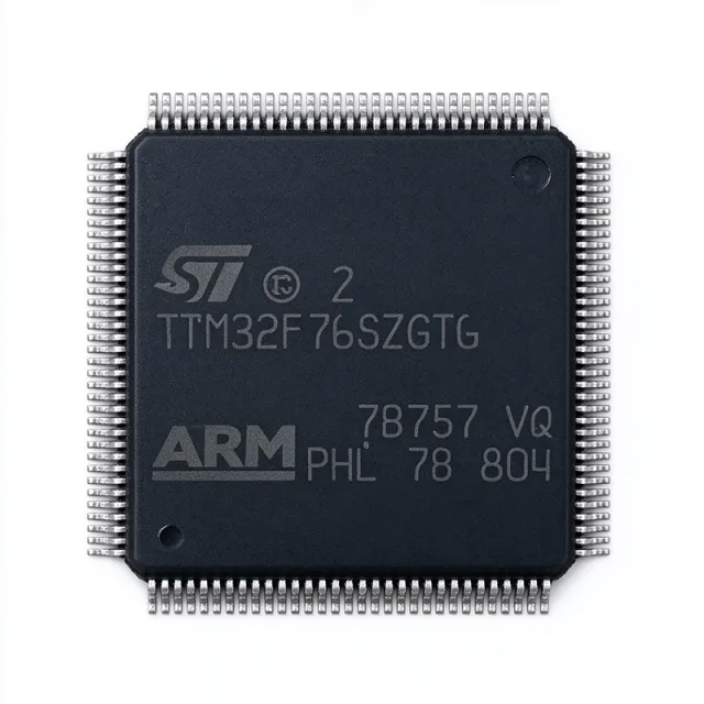
What Is the STM32F765ZGT6 and Is It Available?
The STM32F765ZGT6 is an STMicroelectronics 32-bit ARM Cortex-M7 microcontroller with a double-precision FPU, up to 216 MHz operation, 1 MB of embedded Flash, and 384 KB of SRAM. It is supplied in a 144-LQFP surface-mount package measuring 20 x 20 mm. The device provides 462 DMIPS at 2.14 DMIPS/MHz under Dhrystone 2.1 and includes an ART Accelerator for 0-wait-state Flash execution plus a Chrom-ART DMA2D accelerator. The lifecycle status is active, and the database lists 23,000 units in stock with a minimum order quantity of 1. The verified 1-piece price is $39.375 as of 2026-11-01, declining to $22.9688 at 1,000 pieces as of 2026-11-01.
Engineers can select the STM32F765ZGT6 when a design needs substantial Cortex-M7 throughput, deterministic embedded-Flash execution, mixed analog and digital conversion, and extensive communications without requiring an external FPGA or DSP. Its verified peripheral set includes multiple 12-bit ADCs, a 12-bit DAC, USART, UART, SPI, I2C, CAN, USB OTG FS/HS, an Ethernet MAC with IEEE 1588 support, and an FMC that supports SDRAM, SRAM, and NOR/NAND Flash. The operating range is 1.7 V to 3.6 V at -40 C to +85 C. The STM32F765ZGT6 product page provides the current sourcing entry point, while the XAIPART component catalog supports broader component searches.
Buyer takeaway: The STM32F765ZGT6 is an active, stocked 216 MHz Cortex-M7 with 1 MB Flash and 384 KB SRAM; verify the current distributor quote and lifecycle allocation before releasing a volume order.
How Do You Design In the STM32F765ZGT6?
Start with the verified architecture and memory requirements
The selection begins with the processor, memory, and acceleration features. The Cortex-M7 includes a double-precision FPU and DSP extensions, while the 16 KB I/D L1 cache and ART Accelerator support 0-wait-state execution from embedded Flash. These features make the device suitable for signal processing, control loops, communications gateways, and graphical interfaces where workload scheduling and interrupt response matter.
| Core selection parameter | Verified value |
|---|---|
| Processor | ARM Cortex-M7 with double-precision FPU |
| Maximum CPU frequency | 216 MHz |
| Performance | 462 DMIPS; 2.14 DMIPS/MHz; Dhrystone 2.1 |
| Embedded Flash | 1 MB |
| SRAM | 384 KB |
| L1 cache | 16 KB I/D cache |
| ART Accelerator | Yes; 0-wait-state Flash execution |
| Chrom-ART Accelerator | Yes; DMA2D |
For a firmware-size margin review, use the verified 1 MB Flash value as the starting point rather than estimating from another STM32F7 device. The supplied FAQ also identifies 128 KB of DTCM and AXI-accessible SRAM blocks within the total 384 KB, which helps when partitioning time-critical code and data. If the design later requires a larger code image, the supplied comparison data identifies the STM32F767ZGT6 as a same-footprint option with 2 MB Flash and a hardware crypto/hash block.
Plan the power and analog domains correctly
The device operates across a 1.7 V to 3.6 V supply range. Place a 100 nF decoupling capacitor close to each VDD pin and include a 4.7 uF bulk capacitor on the main supply, as specified in the supplied design guidance. VDDA must connect to VDD through its own ferrite or filtering arrangement when analog peripherals are used. VREF+ is a dedicated ADC reference pin and must be treated as an analog supply node rather than a general-purpose logic output.
| Power or analog item | Verified implementation guidance |
|---|---|
| VDD range | 1.7 V to 3.6 V |
| Per-VDD decoupling | 100 nF close to each VDD pin |
| Main bulk capacitance | 4.7 uF |
| VDDA connection | Tie to VDD with its own ferrite or filter when analog peripherals are in use |
| VREF+ | ADC reference voltage |
| VBAT | RTC backup supply |
| VCAP_1 and VCAP_2 | Core voltage decoupling for the 1.2 V LDO |
Do not infer a specific regulator topology, capacitor tolerance, or analog-noise target from the supplied database. Those values require the complete schematic, board-level return-path plan, and the manufacturer's reference layout. Follow the ST reference layout for the HSE crystal and VREF+ analog domain, and use the verified package data to preserve the 144-LQFP land pattern and 20 x 20 mm body dimensions.
Map the communications and external-memory requirements
The MCU integrates USART, UART, SPI, I2C, CAN, USB OTG FS/HS, and an Ethernet MAC with IEEE 1588. The FMC can connect external SDRAM, SRAM, NOR Flash, or NAND Flash when frame buffers, mass storage, or larger application memory are required. Pin-level planning should preserve access to the two USB peripheral pairs, Ethernet signals, CAN signals, FMC address and data lines, and both SWD programming pins.
| Functional group | Key verified pins or interfaces |
|---|---|
| Debug and boot | PA13/JTMS/SWDIO, PA14/JTCK/SWCLK, BOOT0 |
| Clock backup | PC14/OSC32_IN, PC15/OSC32_OUT, VBAT |
| USB | PA11/OTG_FS_DM and PA12/OTG_FS_DP; PI11/OTG_FS_DM and PA9/OTG_FS_VBUS |
| CAN | PD0/CAN1_RX and PD1/CAN1_TX |
| Ethernet | PC4/PC5/PB0/PB1 receive signals and PG11/ETH_TX_EN |
| External memory | FMC address, data, chip-enable, and clock signals distributed across PF, PG, PD, and PI pins |
The Ethernet MAC requires a board-level network interface design; the supplied application guidance calls for PHY magnetics on the MII/RMII lines. Likewise, use an external Ethernet PHY when the application requires a physical network connection. The MCU's MAC and IEEE 1588 support do not replace the required PHY and passive network components.
Assign analog conversion functions carefully
Use the multiple 12-bit ADCs for sensor acquisition and the 12-bit DAC for analog output. The supplied application data identifies three ADCs and two DACs in the broader peripheral description, with ADC sampling listed as 2.4 MSPS for industrial and medical use cases. Preserve analog trace separation, route VREF+ deliberately, and place the analog supply filtering close to VDDA. The same guidance applies whether the MCU performs motor-current measurement, audio capture, or patient-monitor signal acquisition.
Validate boot, programming, and low-power behavior
BOOT0 controls boot-mode selection, while PA13 and PA14 provide the verified SWD paths for JTMS/SWDIO and JTCK/SWCLK. The device also supports Sleep, Stop, and Standby low-power modes. Confirm the boot configuration, debugger connection, wake behavior, and retention expectations in hardware before production release. The database supports those functions, but it does not provide a complete state-transition or current-consumption table for a final power budget.
Design takeaway: Preserve the 144-LQFP power, analog, debug, boot, and communication pin assignments, follow the supplied decoupling and analog-filtering guidance, and validate timing and power behavior on hardware before production.
Which Alternatives Are Drop-In Choices for the STM32F765ZGT6?
The supplied alternatives data identifies the STM32F769ZGT6 as a same-footprint option in the 144-LQFP package. It retains the 144-LQFP footprint and increases embedded Flash to 2 MB, while its listed distinction is an added MIPI-DSI display interface. That makes it a relevant candidate when a design needs more firmware space or the MIPI-DSI interface, subject to board-level pin-function and firmware verification.
| Parameter | STM32F765ZGT6 | STM32F769ZGT6 |
|---|---|---|
| Manufacturer | STMicroelectronics | STMicroelectronics |
| Package | 144-LQFP, 20 x 20 mm | 144-LQFP |
| Embedded Flash | 1 MB | 2 MB |
| Documented added interface | No MIPI-DSI addition listed | MIPI-DSI display interface |
The STM32F767ZGT6 and STM32F746ZGT6 also appear in the supplied FAQ as ST line variants in the same LQFP-144 footprint. The supplied information states that the F767 has 2 MB Flash and a hardware crypto/hash block, while the F746 has 320 KB SRAM compared with 384 KB in the F765. Those distinctions make them selection candidates, but their complete product specification records are not supplied in the same structured form. They should therefore remain conditional alternatives rather than be represented as fully characterized equivalents in this comparison.
No pin-compatible GigaDevice equivalent is identified in the supplied data. The FAQ instead notes that cross-brand Cortex-M7 choices require layout rework and that ST line variants remain the only identified true drop-ins. A footprint match alone does not establish interchangeability; verify boot pins, power pins, debug access, peripheral multiplexing, clock requirements, and firmware support before approving a second source.
| Alternative decision | Action for the engineering team |
|---|---|
| Same footprint is required | Prioritize ST line variants and verify every multiplexed pin in the schematic. |
| More Flash is required | Evaluate the supplied 2 MB STM32F769ZGT6 option and the STM32F767ZGT6 FAQ entry. |
| MIPI-DSI is required | Evaluate the STM32F769ZGT6 because the supplied alternative data identifies that interface. |
| Cross-brand sourcing is required | Plan for layout rework; do not classify a non-matching pinout as a drop-in. |
Alternative takeaway: Use the STM32F769ZGT6 as the primary same-package alternative in the supplied dataset, then complete a pin-by-pin and firmware review before approving it as a production substitute.
What Does Lifecycle and Supply Data Say About the STM32F765ZGT6?
The STM32F765ZGT6 is active, and the database lists 23,000 units in stock with a minimum order quantity of 1. The verified base price is $22.9688 as of 2026-11-01, which corresponds to the supplied 1,000-piece tier. The exact dated pricing tiers provide a consistent purchasing baseline for cost modeling.
| Quantity threshold | Verified unit price as of 2026-11-01 |
|---|---|
| 1 piece or more | $39.375 |
| 10 pieces or more | $28.4375 |
| 100 pieces or more | $25.1562 |
| 500 pieces or more | $24.0625 |
| 1,000 pieces or more | $22.9688 |
The database's dated tier table differs from the earlier FAQ snapshot: the FAQ lists an approximate 1-piece price of $20.14 as of 2026-10-10, while the newer tier table lists $39.375 as of 2026-11-01. This can reflect the source date, distributor mix, packaging, or quote conditions. For budgeting, use the exact 2026-11-01 tier table and request a live distributor quote rather than combining prices from the two snapshots.
The active lifecycle status supports continued design use, but active status does not guarantee unlimited allocation or stable lead time. Confirm authorized-channel availability, date-code traceability, packaging, RoHS status, and production quantity before committing a long-term BOM. The database confirms RoHS compliance, MOQ of 1, and current stock, but it does not provide a production-life guarantee or a factory allocation schedule. Use the STM32F765ZGT6 product page to refresh the quote and stock position at the point of purchase.
Supply takeaway: The part is active and stocked, but use the exact pricing tiers dated 2026-11-01 for budgeting and secure a live authorized quote before committing a production schedule.
What Should Buyers Watch as Demand Evolves?
The strongest buying signal is the combination of 216 MHz performance, 1 MB Flash, and 384 KB SRAM in one active LQFP-144 device. Buyers should first confirm whether their workload benefits from the Cortex-M7 FPU and DSP instructions rather than merely selecting the part for its clock rate. FFT, FIR, control, and communication-heavy firmware can use the processor and memory resources more effectively than a simpler control workload.
Second, watch firmware-headroom decisions. A 1 MB Flash configuration supports the current design, but the supplied alternatives identify 2 MB devices in the same footprint. If future code growth, OTA duplication, or additional protocol stacks will consume the current margin, evaluate the higher-Flash option before the PCB layout becomes difficult to change. The comparison remains valid only after confirming that the selected variant preserves the required peripheral assignments.
Third, plan external-memory expansion deliberately. The FMC supports SDRAM, SRAM, NOR Flash, and NAND Flash, giving a path for larger frame buffers or storage. The supplied HMI and gateway application records demonstrate why the combination of DMA2D, Ethernet, USB, and FMC matters, but they do not eliminate the need to calculate memory bandwidth, bus loading, and interface timing. The CuprumFlow Graphics article on HD MCU interfaces provides additional context for UI-focused design evaluation.
Fourth, consider power and I/O scaling together. The 1.7 V to 3.6 V operating range supports integration with a 3.3 V supply plan, while the -40 C to +85 C rating covers the verified industrial ambient range. At the same time, USB, Ethernet, FMC, analog conversion, and high-rate DSP workloads can change system power and thermal requirements. Do not calculate the device-level power budget without the missing operating-current data for the selected mode, clock configuration, and peripheral set.
Finally, monitor firmware-tool and prototyping practices. The ESP-Mosaico AI coding article on microcontroller prototyping highlights the broader movement toward assisted embedded development, while the STM32F765ZGT6 remains governed by its ST device support and package-specific constraints. Generated code still requires review against the verified pin definitions, clock plan, memory map, and peripheral configuration. Start with the XAIPART component catalog to check related parts, and use the exact MPN when requesting quotes or reviewing stock.
Outlook takeaway: Prioritize FPU and DSP utilization, preserve firmware and external-memory expansion options, and treat live pricing and allocation—not nominal headline performance—as the immediate sourcing variables.
Yorumlar
İlk yorumu yapın.
🔐 Lütfen giriş yap bir yorum göndermek için.
Hesabınız yok mu? Kayıt ol