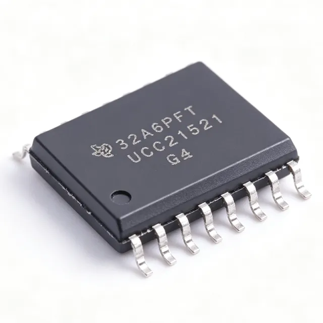
UCC21521DWR - 4A/6A 5.7kVrms Isolated Gate Driver | TI
MPN: UCC21521DWR ✓ فعالUCC21521DWR جائزہ
An isolated gate driver is a power-management IC that translates low-voltage control logic from a microcontroller or DSP into the high peak current required to switch power transistors, while maintaining galvanic isolation between the control side and the power stage. Within the power-electronics hierarchy it sits between PWM controllers and MOSFETs, IGBTs, or SiC MOSFETs, and it is essential for safety isolation and noise immunity in high-voltage converters.
Key features include 19-ns typical propagation delay, 5-ns maximum channel-to-channel matching, 6-ns maximum pulse-width distortion, and a 10-ns minimum input pulse width. These tight timing specifications reduce switching losses and minimize shoot-through risk. The DIS enable pin supports power sequencing and fast fault shutdown, and programmable dead time (for half-bridge configurations) prevents cross-conduction.
Technically, the UCC21521 uses TI capacitive isolation technology to deliver the 5.7-kV RMS reinforced barrier with CMTI of at least 100 V/ns, making it robust in high dv/dt SiC environments. Input thresholds are TTL and CMOS compatible for direct 3.3-V logic interfacing, and an 8-V UVLO protects the power switch from under-driven operation.
Typical applications include motor drives, solar string inverters, EV onboard chargers, and isolated DC-DC converters, where the 4-A/6-A drive strength and up-to-5-MHz switching capability suit SiC and IGBT power stages.
Design tip: place decoupling capacitors directly at VCCI and VDDA/VDDB pins and minimize gate-loop inductance to achieve the datasheet timing figures and avoid dv/dt-induced false triggering.
This page adds value beyond the datasheet with drop-in alternative comparisons, pricing tiers, and practical layout notes synthesized from distributor and manufacturer data.
کے لیے ڈراپ اِن متبادل UCC21521DWR — یکساں پیکیج، پن سے پن مطابقت پذیر۔ مختلف پیکیج والے پرزے جن کے لیے PCB دوبارہ کام درکار ہو، شامل نہیں ہیں۔
اس سیریز میں مختلف ورژن
اسی سیریز کے ماڈلز جو ڈراپ اِن مطابقت رکھتے ہیں UCC21521DWR (یکساں فارم فیکٹر اور فٹ پرنٹ) — میں مختلف Package, Isolation Rating, Isolation Technology, Enable Pin, Isolation Type.
UCC21521ADWR
✅ ڈراپ-اِنقیمت کے لیے رابطہ کریں
ڈیٹا شیٹ دیکھیں →UCC21521Q-Q1
✅ ڈراپ-اِنقیمت کے لیے رابطہ کریں
ڈیٹا شیٹ دیکھیں →UCC21521DWR
✅ ڈراپ-اِنقیمت کے لیے رابطہ کریں
ڈیٹا شیٹ دیکھیں →UCC21540
✅ ڈراپ-اِن ⚠️ تفصیلات غیر تصدیق شدہقیمت کے لیے رابطہ کریں
ڈیٹا شیٹ دیکھیں →UCC21520
✅ ڈراپ-اِن ⚠️ تفصیلات غیر تصدیق شدہقیمت کے لیے رابطہ کریں
ڈیٹا شیٹ دیکھیں →UCC21550BDWR
✅ ڈراپ-اِن ⚠️ تفصیلات غیر تصدیق شدہقیمت کے لیے رابطہ کریں
ڈیٹا شیٹ دیکھیں →UCC21521DWR زیادہ سے زیادہ ریٹنگز اور برقی خصوصیات
| Number of Channels | 2 |
| Peak Output Source Current | 4 A |
| Peak Output Sink Current | 6 A |
| Isolation Rating | 5700 Vrms (reinforced) |
| Common-Mode Transient Immunity (CMTI) | >= 100 V/ns |
| Propagation Delay (typical) | 19 ns |
| Channel Matching (max) | 5 ns |
| Pulse-Width Distortion (max) | 6 ns |
| Minimum Input Pulse Width | 10 ns |
| Output Supply UVLO | 8 V |
| Switching Frequency (max) | 5 MHz |
| Driver Configuration | Dual low-side / dual high-side / half-bridge (universal) |
| این ایبل پن | Yes (DIS, disable) |
| Input Threshold Compatibility | TTL / CMOS compatible (3.3 V logic) |
| آپریٹنگ درجہ حرارت | -40C to +125C |
| پیکیج | 16-pin SOIC (DW) |
| ماؤنٹنگ ٹائپ | Surface Mount |
| Isolation Technology | Capacitive isolation |
UCC21521DWR پن کنفیگریشن
| پن 1 | VCCI — 3.3-V to 5-V input-side supply |
| پن 2 | GND — Input-side ground reference |
| پن 3 | DIS — Disable input (enable/disable pin) |
| پن 4 | IN_A — Input signal, channel A |
| پن 5 | IN_B — Input signal, channel B |
| پن 6 | NC — Not connected (per datasheet) |
| پن 7 | NC — Not connected (per datasheet) |
| پن 8 | NC — Not connected (per datasheet) |
| پن 9 | NC — Not connected (per datasheet) |
| پن 10 | NC — Not connected (per datasheet) |
| پن 11 | VDDA — Output driver A supply |
| پن 12 | OUTA — Gate drive output, channel A |
| پن 13 | GNDA — Output-side ground reference A |
| پن 14 | GNDB — Output-side ground reference B |
| پن 15 | OUTB — Gate drive output, channel B |
| پن 16 | VDDB — Output driver B supply |
عام استعمالات
UCC21521DWR کے لیے موزوں ہے 6 ایپلیکیشنs: Three-Phase Motor Drives, Solar String Inverters, EV Onboard Chargers and OBC/DC-DC, Isolated DC-DC Converters, SiC MOSFET Power Modules, Industrial Power Supplies and Welders.
Three-Phase Motor Drives
In industrial three-phase inverters, each leg of the power stage requires an isolated half-bridge gate driver, and the UCC21521DWR fits this role with 4-A source / 6-A sink peak current that quickly charges and discharges IGBT or SiC MOSFET gate capacitances, reducing switching losses. The 5.7-kV RMS reinforced barrier isolates the low-voltage MCU from the high-voltage DC bus for safety compliance, while CMTI of at least 100 V/ns keeps the driver immune to the large dv/dt at the switching node. Its programmable dead time prevents shoot-through between high- and low-side switches, and the DIS enable pin allows instant shutdown on fault detection from the motor-control DSP. Positioned between a 3.3-V PWM controller and the gate networks, it delivers the timing precision (5-ns matching) needed for balanced phase currents.
تجویز کردہ
Solar String Inverters
Grid-tied solar string inverters combine a boost stage and a DC-AC bridge where the UCC21521DWR provides isolated gate drive for the high-side and low-side power switches. The 5.7-kV RMS reinforced isolation supports the system-level insulation requirements between PV input, AC grid, and control electronics. Its 19-ns propagation delay and 100 V/ns CMTI are well matched to SiC MOSFET switching in the 20-100 kHz range, where high dv/dt on the switching node would falsely trigger weaker isolation technologies. The 8-V UVLO ensures the SiC devices are never driven below their minimum recommended gate voltage, preventing operation in a high-Rds(on) regime that causes thermal runaway. The enable pin lets the inverter controller gate off all bridges within nanoseconds during grid faults or MPPT transients.
تجویز کردہ
EV Onboard Chargers and OBC/DC-DC
Electric-vehicle onboard chargers use PFC plus isolated LLC stages that switch at high frequency, and the UCC21521DWR supports this with operation up to 5 MHz and a 10-ns minimum pulse width, enabling compact high-frequency magnetics. The 4-A/6-A drive strength handles the large gate charge of SiC MOSFETs typical in 6.6-kW to 22-kW OBC designs, while the 5.7-kV RMS barrier satisfies isolation between the traction battery and AC mains. The -40C to +125C operating range covers under-hood and near-battery thermal environments. Its tight 5-ns channel matching keeps LLC bridges symmetric, minimizing transformer flux imbalance. For automotive-qualified builds, the UCC21521Q-Q1 variant adds AEC-Q100 compliance without PCB changes.
تجویز کردہ
Isolated DC-DC Converters
Telecom and industrial isolated DC-DC converters (half-bridge and full-bridge LLC topologies) use the UCC21521DWR to drive primary-side power switches with galvanic isolation from the control loop. The 19-ns typical propagation delay and 6-ns maximum pulse-width distortion preserve duty-cycle accuracy at the 100 kHz-1 MHz switching frequencies these converters use, directly reducing output ripple and improving transient response. The 100 V/ns CMTI is essential in LLC bridges where the midpoint slews rapidly every cycle. With the DIS pin, a supervisory circuit can disable both outputs during start-up sequencing or overcurrent events. The dual-input architecture supports both dual low-side and half-bridge configurations, letting one driver IC serve multiple converter topologies across a product family.
تجویز کردہ
SiC MOSFET Power Modules
SiC-based power modules in traction inverters, energy storage converters, and high-power supplies demand gate drivers with high CMTI and strong sink current, and the UCC21521DWR delivers both: at least 100 V/ns common-mode transient immunity and a 6-A pull-down that holds SiC gates firmly low against Miller-induced turn-on. The 8-V UVLO is deliberately matched to SiC gate-drive levels, blocking operation until VDDA/VDDB is adequate. Its capacitive isolation technology maintains the 5.7-kV RMS reinforced rating across temperature and aging, supporting the functional-safety isolation of high-voltage stages. The universal input architecture lets the same component drive dual low-side switches in boost PFC or a high/low-side half-bridge in the inverter stage of the same system.
تجویز کردہ
Industrial Power Supplies and Welders
High-power industrial AC-DC supplies, welding inverters, and induction-heating converters rely on the UCC21521DWR for robust isolated gate drive in electrically noisy environments. The reinforced 5.7-kV RMS isolation separates operator-accessible controls from hazardous voltages, while the TTL/CMOS-compatible inputs connect directly to 3.3-V controllers without level shifting. Its 4-A/6-A peak currents switch large IGBT modules efficiently at the 20-50 kHz frequencies typical of welding inverters, and the 100 V/ns CMTI withstands the severe dv/dt generated by hard-switched current ramps. The enable pin provides a fast, deterministic shutdown path for the overcurrent and overtemperature protection loops required in these high-energy systems, complementing module-level desaturation protection.
تجویز کردہ
تجویز کردہ پروڈکٹس کا خلاصہ
کے لیے انجینئرنگ ریفرنس ڈیٹا UCC21521DWR — موازنہ، ڈیزائن رہنمائی، اور تعمیل کی معلومات۔
انتخاب کی گائیڈ
متبادلات کے ساتھ موازنہ
| پیرامیٹر | یہ پروڈکٹ | UCC21521ADWR | UCC21521Q-Q1 | UCC21520 | UCC21540 | UCC21550BDWR |
|---|---|---|---|---|---|---|
| Package | 16-SOIC (DW) | 16-SOIC (DW) - same | 16-SOIC (DW) - same | 16-SOIC (DW) - same | 16-SOIC (DW) - same | 16-SOIC (DW) - same |
| Brand | Texas Instruments | Texas Instruments | Texas Instruments | Texas Instruments | Texas Instruments | Texas Instruments |
| Automotive Grade | No | No | Yes (AEC-Q100) | No | Q1 variant available | B-grade variant available |
اہم امتیازی خصوصیات
- Enable (DIS) pin for fast fault shutdown (بمقابلہUCC21520)
- AEC-Q100 automotive option on the same footprint (بمقابلہUCC21521Q-Q1)
- 4-A source / 6-A sink asymmetric drive (بمقابلہUCC21520)
ڈیزائن نوٹس
Place a 0.1-uF ceramic capacitor in parallel with a bulk capacitor directly across VCCI-GND, and identical pairs across VDDA-GNDA and VDDB-GNDB, within 2-3 mm of the pins. Because the two output grounds (GNDA/GNDB) are separate, route their returns individually back to their respective power-stage source terminals rather than tying them near the IC, which defeats the intended isolation. On a 4-layer board, use an uninterrupted ground plane on layer 2 and stitch the input-side ground region away from the output-side switching copper.
Minimize the gate loop: keep the OUTA/OUTB trace to the MOSFET gate and the return path via GNDA/GNDB as short and wide as possible; every nH of loop inductance causes gate ringing with a 4-A/6-A drive. Add a small external gate resistor (2-10 ohm typical) to damp ringing and control switching speed, and optionally a pull-down resistor (10 kohm) at each gate to hold SiC MOSFETs off while VDDA/VDDB is below the 8-V UVLO threshold during start-up.
Even with 100 V/ns CMTI, careless layout can couple dv/dt into input-side signals. Route the IN_A/IN_B and DIS traces away from the switching node and away from the isolation gap crossing; do not run control traces under or adjacent to OUTA/OUTB copper. Also note the DIS pin must be actively driven or biased to a defined level - leaving it floating can produce undefined enable states at power-up; a pull-up or pull-down resistor consistent with the required default state is best practice.
Estimated: gate-drive dissipation per channel is Qg x fsw x VDD; for example a SiC MOSFET with 60-nC gate charge at 100 kHz and 18-V drive dissipates about 0.11 W per channel in the driver plus resistor losses. The 16-SOIC (DW) package handles this without heatsinking, but verify junction temperature stays below +125C by accounting for driver quiescent power and layout copper area on VDDA/VDDB nets.
تعمیل کی معلومات
Standard TI UCC21521 (DWR suffix) is RoHS-compliant and lead-free per TI product page. Automotive AEC-Q100 qualification applies to the UCC21521Q-Q1 variant, not this part number. REACH and halogen-free status not stated in provided data.







