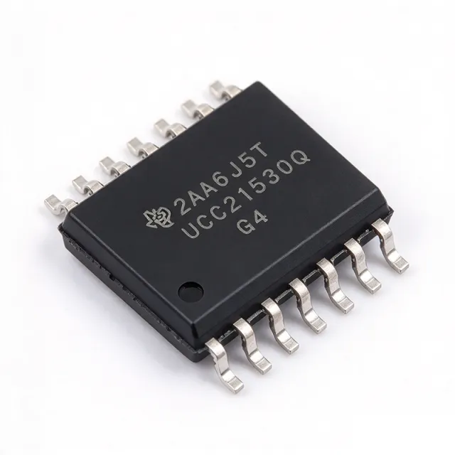
UCC21530QDWKRQ1 - 4A/6A 5.7kVrms Isolated Gate Driver | TI
MPN: UCC21530QDWKRQ1 ✓ فعال| مقدار | فی یونٹ قیمت | کل رقم |
|---|---|---|
| 1 | $1.8281 | $1.83 |
| 10 | $1.3203 | $13.20 |
| 100 | $1.168 | $116.80 |
| 500 | $1.1172 | $558.60 |
| 1,000 | $1.0664 | $1,066.40 |
UCC21530QDWKRQ1 جائزہ
An isolated gate driver is a switching power-supply sub-system that translates low-side logic-level PWM into a high-voltage, floating gate-drive signal referenced to the switched-node of a half-bridge. It belongs to the gate-driver IC family, a category within power MOSFET/IGBT drivers, under the broader power management hierarchy. The UCC21530-Q1 integrates a silicon-oxide isolation transformer, two output channels (the chip itself), and is AEC-Q100-qualified for automotive environments by design.
Key features include 4-A peak source and 6-A peak sink output current, a wide 18-V to 25-V VDD/VDDA range (3-V to 18-V on logic side), 33-ns typical propagation delay, 5-ns maximum channel-to-channel delay matching, 100-V/ns CMTI, and integrated programmable deadtime (DT) for shoot-through prevention. An active-low enable pin and a fault-ready open-drain output support sequencing and desaturation monitoring in three-phase inverters and PFC stages.
Typical applications include traction inverters for EV powertrains, on-board chargers (OBC), industrial servo drives, solar string inverters, telecom DC/DC converters, and any 400-V / 800-V bus half-bridge topology requiring reinforced isolation. The DWK wide-body SOIC package provides 8.5 mm of creepage for high-voltage pollution-degree-2 environments.
When designing with the UCC21530-Q1, place 1-uF / 100-nF decoupling on VDD/VDDA/VCCI close to the IC pins. Use a bootstrap diode + capacitor on the high-side channel whose voltage rating is rated for the DC bus plus transient ringing. Always respect the absolute-maximum VDD/VDDA of 30 V to avoid catastrophic gate-oxide damage.
This page synthesizes distributor pricing, drop-in alternatives, and practical design notes not consolidated in the manufacturer datasheet — including same-package TI options, cross-brand validation notes, and BOM-optimization guidance unavailable on DigiKey/Mouser product pages.
کے لیے ڈراپ اِن متبادل UCC21530QDWKRQ1 — یکساں پیکیج، پن سے پن مطابقت پذیر۔ مختلف پیکیج والے پرزے جن کے لیے PCB دوبارہ کام درکار ہو، شامل نہیں ہیں۔
اس سیریز میں مختلف ورژن
اسی سیریز کے ماڈلز جو ڈراپ اِن مطابقت رکھتے ہیں UCC21530QDWKRQ1 (یکساں فارم فیکٹر اور فٹ پرنٹ) — میں مختلف Package, Operating Temperature Range, Common-Mode Transient Immunity (CMTI), Peak Sink Current, Peak Source Current.
فوری موازنہ ٹول — ساتھ ساتھ موازنے کے لیے متبادل پرزے منتخب کریں:
UCC21530DWKR
قیمت کے لیے رابطہ کریں
ڈیٹا شیٹ دیکھیں →SI8273ABD
قیمت کے لیے رابطہ کریں
ڈیٹا شیٹ دیکھیں →UCC21530DWKR
قیمت کے لیے رابطہ کریں
ڈیٹا شیٹ دیکھیں →UCC21530QDWKQ1
📋 حوالہ جاتی متبادل (کیٹلاگ میں نہیں)
UCC21530ADWR
📋 حوالہ جاتی متبادل (کیٹلاگ میں نہیں)
UCC21530ADQKRQ1
📋 حوالہ جاتی متبادل (کیٹلاگ میں نہیں)
SI8271AB-IM
📋 حوالہ جاتی متبادل (کیٹلاگ میں نہیں)
UCC21530QDWKRQ1 زیادہ سے زیادہ ریٹنگز اور برقی خصوصیات
| فنکشن | Isolated dual-channel gate driver |
| Number of Channels | 2 (high-side / low-side) |
| Peak Source Current | 4 A |
| Peak Sink Current | 6 A |
| Isolation Voltage (RMS) | 5.7 kVRMS |
| Channel-to-Channel Spacing | 3.3 mm (minimum) |
| Creepage / Clearance | 8.5 mm (DWK wide-body) |
| VDD/VDDA Supply Range | 18 V to 25 V (3 V to 18 V on logic side per datasheet) |
| Propagation Delay (Typical) | 33 ns |
| Maximum Operating Frequency | 5 MHz |
| Common-Mode Transient Immunity (CMTI) | 100 V/ns (minimum) |
| Programmable Deadtime | Yes (DT pin) |
| این ایبل پن | Yes (active-low) |
| آپریٹنگ درجہ حرارت رینج | -40C to +125C |
| پیکیج | 14-pin SOIC (DWK wide-body) |
| ماؤنٹنگ ٹائپ | Surface Mount |
| MSL لیول | 2 |
| AEC-Q100 Qualification | Qualified |
| RoHS اسٹیٹس | Compliant |
| Logic Input Compatibility | CMOS / TTL |
UCC21530QDWKRQ1 پن کنفیگریشن
| پن 1 | VDD1 — Logic-side supply, 3V to 18V |
| پن 2 | GND1 — Logic-side ground reference |
| پن 3 | INA — Channel A PWM input (non-inverting) |
| پن 4 | INB — Channel B PWM input (non-inverting) |
| پن 5 | DISABLE — Active-low enable for both channels |
| پن 6 | NC — Not connected (per datasheet) |
| پن 7 | DT — Programmable deadtime (resistor to GND1) |
| پن 8 | NC — Not connected (per datasheet) |
| پن 9 | OUTA — Channel A gate-drive output |
| پن 10 | VDDA — Channel A driver supply, 18V to 25V |
| پن 11 | VDDB — Channel B driver supply, 18V to 25V |
| پن 12 | OUTB — Channel B gate-drive output |
| پن 13 | VS — Channel B high-side return (switched node) |
| پن 14 | VB — Channel B high-side floating supply (bootstrap) |
عام استعمالات
UCC21530QDWKRQ1 کے لیے موزوں ہے 6 ایپلیکیشنs: EV Traction Inverter Half-Bridge, On-Board Charger (OBC) PFC Stage, Industrial Servo Drive Three-Phase Inverter, Solar String Inverter Half-Bridge, Telecom DC/DC Converter Full-Bridge, Three-Phase GaN Motor Drive.
EV Traction Inverter Half-Bridge
The UCC21530QDWKRQ1 drives 800-V bus SiC MOSFET half-bridges in EV traction inverters, where its 5.7-kVRMS reinforced isolation with 8.5-mm creepage exceeds IEC 60747-17 working-voltage requirements. The 4-A peak source / 6-A peak sink current switches 1200-V SiC MOSFETs at 50-100 kHz with sub-5-ns channel-to-channel delay matching, minimizing deadtime losses. The AEC-Q100 Grade 1 qualification with 100-V/ns CMTI rejects the fast dV/dt of SiC switching nodes, preventing logic-side latch-up. Placed between the low-voltage MCU and the high-voltage bus, it enables motor torque control at 20 kHz PWM with reinforced isolation per UL 1577.
تجویز کردہ
On-Board Charger (OBC) PFC Stage
In a 6.6-kW or 11-kW OBC power-factor-correction stage, the UCC21530QDWKRQ1 drives the interleaved totem-pole PFC MOSFETs with reinforced isolation, allowing the digital controller to operate safely referenced to chassis ground. Its 33-ns typical propagation delay and 5-ns channel-to-channel matching enable high-frequency GaN switching at 100-500 kHz with tight duty-cycle control and low THD. The 18-V to 25-V VDD/VDDA range directly accepts a regulated 18-V aux winding without a separate LDO, simplifying the BOM. Programmable deadtime via the DT pin prevents shoot-through during AC zero-crossing transitions.
تجویز کردہ
Industrial Servo Drive Three-Phase Inverter
The UCC21530QDWKRQ1 drives the three-phase IGBT inverter of a 480-V AC industrial servo drive, where the reinforced isolation allows a single low-voltage FPGA/MCU to control all three half-bridges without opto-couplers. The 4-A source current charges 1.2-kV/50-A IGBT gates in <500 ns at 8 kHz PWM, while the 100-V/ns CMTI rejects the high dV/dt of the IGBT collector transitions. Integrated programmable deadtime prevents cross-conduction during 2-us deadtime windows. The AEC-Q100 qualification provides additional reliability margin in factory environments up to +85C ambient.
تجویز کردہ
Solar String Inverter Half-Bridge
In 1500-V DC solar string inverters, the UCC21530QDWKRQ1 drives the boost and full-bridge SiC stages with reinforced isolation that exceeds the 1500-V DC working voltage plus transient over-voltage. The 5-MHz switching capability supports GaN-based high-frequency stages targeting 99% efficiency, while the 4-A/6-A drive current easily switches large 62-mm SiC modules. The wide VDD/VDDA range (18 V to 25 V) accepts a 20-V aux winding directly, eliminating an extra LDO stage. AEC-Q100 qualification provides field-replacement value in outdoor enclosures.
تجویز کردہ
Telecom DC/DC Converter Full-Bridge
The UCC21530QDWKRQ1 drives the primary-side full-bridge of a 48-V to 400-V/1-kW telecom DC/DC converter with reinforced isolation per IEC 62368-1. The 4-A source current switches the primary MOSFETs at 100-200 kHz with tight timing, while the 33-ns propagation delay supports the closed-loop peak-current-mode control. The 100-V/ns CMTI rejects the high dV/dt of the isolation transformer primary, and the DWK wide-body package provides the 8.5-mm creepage needed for the reinforced barrier.
تجویز کردہ
Three-Phase GaN Motor Drive
The UCC21530QDWKRQ1 drives GaN half-bridges in a 48-V to 400-V three-phase motor drive where switching frequencies of 100 kHz to 1 MHz demand sub-50-ns propagation delay and 5-ns channel matching. Its reinforced 5.7-kVRMS isolation allows a low-voltage MCU/FPGA to control the high-voltage bus safely, while the 4-A/6-A drive strength charges GaN gates in <20 ns for the lowest switching losses. AEC-Q100 qualification supports automotive e-compressor and e-turbo applications operating in harsh -40C to +125C environments.
تجویز کردہ
تجویز کردہ پروڈکٹس کا خلاصہ
کے لیے انجینئرنگ ریفرنس ڈیٹا UCC21530QDWKRQ1 — موازنہ، ڈیزائن رہنمائی، اور تعمیل کی معلومات۔
انتخاب کی گائیڈ
متبادلات کے ساتھ موازنہ
| پیرامیٹر | یہ پروڈکٹ | UCC21530DWK | UCC21530QDWKQ1 | UCC21530DWKR | SI8271AB-IM | SI8273ABD |
|---|---|---|---|---|---|---|
| Brand | Texas Instruments | Texas Instruments | Texas Instruments | Texas Instruments | Silicon Labs | Silicon Labs |
| Package | 14-SOIC (DWK wide-body) | 14-SOIC (DWK wide-body) - same | 14-SOIC (DWK wide-body) - same | 14-SOIC (DWK wide-body) - same | 14-SOIC (wide-body) - same footprint | 14-SOIC (wide-body) - same footprint |
| Peak Source Current | 4 A | 4 A | 4 A | 4 A | 4 A | 4 A |
| Peak Sink Current | 6 A | 6 A | 6 A | 6 A | 4 A | 4 A |
| Isolation Voltage | 5.7 kVRMS | 5.7 kVRMS | 5.7 kVRMS | 5.7 kVRMS | 5 kVRMS | 5 kVRMS |
| AEC-Q100 | Qualified | Not qualified | Qualified | Not qualified | Not qualified (industrial only) | Not qualified (industrial only) |
| Programmable Deadtime | Yes | Yes | Yes | Yes | No (fixed internal) | Yes (DT pin) |
| Propagation Delay | 33 ns (typical) | 33 ns | 33 ns | 33 ns | 60 ns (typical) | 50 ns (typical) |
| CMTI (minimum) | 100 V/ns | 100 V/ns | 100 V/ns | 100 V/ns | 50 V/ns | 50 V/ns |
اہم امتیازی خصوصیات
- Reinforced 5.7-kVRMS isolation with 8.5-mm creepage in a single SOIC-14 wide-body package (بمقابلہUCC21222QDRQ1)
- AEC-Q100 Grade 1 qualification for automotive applications (بمقابلہUCC21530DWK (industrial variant))
- 100-V/ns minimum CMTI with 33-ns propagation delay (بمقابلہSI8271AB-IM (Silicon Labs))
ڈیزائن نوٹس
Bootstrap design for the high-side channel: the VB-VS pin pair must be charged through a fast-recovery bootstrap diode whenever the low-side switch pulls VS below ground. Estimated: at 100 kHz, 4-A source current, and 50-nC gate charge, choose Cboot >= 10x Qg so a 470-nF to 1-uF ceramic rated for 50 V is typical. Use a diode with reverse voltage >= VDD + ringing. Refresh the bootstrap on every switching cycle or VBS undervoltage lockout will engage.
The UCC21530-Q1 dissipates power equal to VDD x Iqu (logic) plus switching losses in the gate-drive path (Qg x Vgs x Fsw per channel). Estimated: at 100 kHz, 50-nC Qg, and 18-V VDD, switching losses are 0.09 W per channel. The DWK wide-body SOIC has theta_JA ~70 C/W on a 1-oz 4-layer PCB, so junction rise is ~6.3 C/W above ambient — easily handled. For continuous 1-A DC drive, the dominant loss is Iqu's supply current; ensure VDD aux winding is current-rated to 100 mA minimum.
PCB layout is critical for reinforced isolation. The DWK wide-body package provides 8.5 mm of internal creepage; the PCB must maintain at least the same creepage distance from any logic-side copper to any driver-side copper across the isolation barrier, including underneath the IC body. Use a slot in the PCB to extend creepage if needed. Place 1-uF bulk + 100-nF ceramic decoupling on VDD1/VDDA/VDDB/VB/VCCI close to the IC pins, and keep the high-current gate-drive loop area to <1 cm^2 to minimize parasitic inductance.
Do not exceed the absolute-maximum VDD/VDDA/VDDB of 30 V — this destroys the gate-oxide of the driver output stage. Do not route logic signals across the isolation barrier with insufficient creepage. The DISABLE pin is active-low; tie to VCCI (logic high) for normal operation. The DT pin sets deadtime via a resistor to GND1 — leaving it floating disables the programmable deadtime and reverts to the internal default. Use only the TI datasheet SLUSD11 reference layout as a starting point.
The UCC21530-Q1 has 100-V/ns minimum CMTI, so it tolerates the high dV/dt of SiC and GaN switching nodes. However, ensure that the gate-drive loop inductance is minimized to keep the gate ringing below VDD + ringing margin. Estimated: a 5-nH loop with 4-A peak current switching in 20 ns produces 5-V overshoot — within the 30-V abs-max for VDD=18 V but may require a gate-source resistor or ferrite bead for safety margin. Always measure VS and VBS waveforms with a high-bandwidth probe before finalizing the design.
تعمیل کی معلومات
AEC-Q100 Grade 1 qualified per TI datasheet SLUSD11. RoHS and REACH compliant per TI product page. Reinforced isolation rated to 5.7 kVRMS per UL 1577 and IEC 60747-17.







