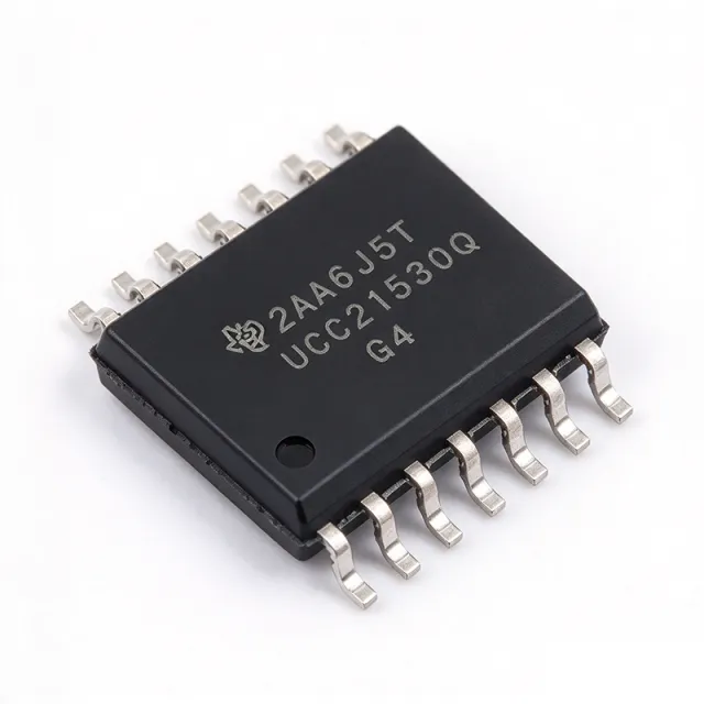
UCC21530QDWKRQ1 - 4A/6A 5.7kVrms Isolated Gate Driver | TI
部品番号: UCC21530QDWKRQ1 ✓ 生産中| 数量 | 単価 | 小計 |
|---|---|---|
| 1 | $1.8281 | $1.83 |
| 10 | $1.3203 | $13.20 |
| 100 | $1.168 | $116.80 |
| 500 | $1.1172 | $558.60 |
| 1,000 | $1.0664 | $1,066.40 |
UCC21530QDWKRQ1 概要
An isolated gate driver is a switching power-supply sub-system that translates low-side logic-level PWM into a high-voltage, floating gate-drive signal referenced to the switched-node of a half-bridge. It belongs to the gate-driver IC family, a category within power MOSFET/IGBT drivers, under the broader power management hierarchy. The UCC21530-Q1 integrates a silicon-oxide isolation transformer, two output channels (the chip itself), and is AEC-Q100-qualified for automotive environments by design.
Key features include 4-A peak source and 6-A peak sink output current, a wide 18-V to 25-V VDD/VDDA range (3-V to 18-V on logic side), 33-ns typical propagation delay, 5-ns maximum channel-to-channel delay matching, 100-V/ns CMTI, and integrated programmable deadtime (DT) for shoot-through prevention. An active-low enable pin and a fault-ready open-drain output support sequencing and desaturation monitoring in three-phase inverters and PFC stages.
Typical applications include traction inverters for EV powertrains, on-board chargers (OBC), industrial servo drives, solar string inverters, telecom DC/DC converters, and any 400-V / 800-V bus half-bridge topology requiring reinforced isolation. The DWK wide-body SOIC package provides 8.5 mm of creepage for high-voltage pollution-degree-2 environments.
When designing with the UCC21530-Q1, place 1-uF / 100-nF decoupling on VDD/VDDA/VCCI close to the IC pins. Use a bootstrap diode + capacitor on the high-side channel whose voltage rating is rated for the DC bus plus transient ringing. Always respect the absolute-maximum VDD/VDDA of 30 V to avoid catastrophic gate-oxide damage.
This page synthesizes distributor pricing, drop-in alternatives, and practical design notes not consolidated in the manufacturer datasheet — including same-package TI options, cross-brand validation notes, and BOM-optimization guidance unavailable on DigiKey/Mouser product pages.
ドロップイン代替品: UCC21530QDWKRQ1 — 同一パッケージでピン互換。PCBの作り直しが必要な異なるパッケージの部品は除外されています。
このシリーズのバリエーション
同一シリーズでドロップイン互換のモデル: UCC21530QDWKRQ1 (同一形状・フットプリント) — 相違点: Package, Operating Temperature Range, Common-Mode Transient Immunity (CMTI), Peak Sink Current, Peak Source Current.
クイック比較ツール — 並列比較する代替部品を選択:
UCC21530DWKR
✓ 在庫あり
$1.95 / 個
データシートを見る →SI8273ABD
✓ 在庫あり
$3.05 / 個
データシートを見る →UCC21530DWKR
✓ 在庫あり
$1.95 / 個
データシートを見る →UCC21530QDWKQ1
📋 参考代替品(カタログ未掲載)
UCC21530ADWR
📋 参考代替品(カタログ未掲載)
UCC21530ADQKRQ1
📋 参考代替品(カタログ未掲載)
SI8271AB-IM
📋 参考代替品(カタログ未掲載)
UCC21530QDWKRQ1 最大定格&電気的特性
| 機能 | Isolated dual-channel gate driver |
| Number of Channels | 2 (high-side / low-side) |
| Peak Source Current | 4 A |
| Peak Sink Current | 6 A |
| Isolation Voltage (RMS) | 5.7 kVRMS |
| Channel-to-Channel Spacing | 3.3 mm (minimum) |
| Creepage / Clearance | 8.5 mm (DWK wide-body) |
| VDD/VDDA Supply Range | 18 V to 25 V (3 V to 18 V on logic side per datasheet) |
| Propagation Delay (Typical) | 33 ns |
| Maximum Operating Frequency | 5 MHz |
| Common-Mode Transient Immunity (CMTI) | 100 V/ns (minimum) |
| Programmable Deadtime | Yes (DT pin) |
| イネーブルピン | Yes (active-low) |
| 動作温度範囲 | -40C to +125C |
| パッケージ | 14-pin SOIC (DWK wide-body) |
| 実装タイプ | Surface Mount |
| MSLレベル | 2 |
| AEC-Q100 Qualification | Qualified |
| RoHS ステータス | Compliant |
| Logic Input Compatibility | CMOS / TTL |
UCC21530QDWKRQ1 ピン構成
| ピン 1 | VDD1 — Logic-side supply, 3V to 18V |
| ピン 2 | GND1 — Logic-side ground reference |
| ピン 3 | INA — Channel A PWM input (non-inverting) |
| ピン 4 | INB — Channel B PWM input (non-inverting) |
| ピン 5 | DISABLE — Active-low enable for both channels |
| ピン 6 | NC — Not connected (per datasheet) |
| ピン 7 | DT — Programmable deadtime (resistor to GND1) |
| ピン 8 | NC — Not connected (per datasheet) |
| ピン 9 | OUTA — Channel A gate-drive output |
| ピン 10 | VDDA — Channel A driver supply, 18V to 25V |
| ピン 11 | VDDB — Channel B driver supply, 18V to 25V |
| ピン 12 | OUTB — Channel B gate-drive output |
| ピン 13 | VS — Channel B high-side return (switched node) |
| ピン 14 | VB — Channel B high-side floating supply (bootstrap) |
主な用途
UCC21530QDWKRQ1 の用途: 6 件s: EV Traction Inverter Half-Bridge, On-Board Charger (OBC) PFC Stage, Industrial Servo Drive Three-Phase Inverter, Solar String Inverter Half-Bridge, Telecom DC/DC Converter Full-Bridge, Three-Phase GaN Motor Drive.
EV Traction Inverter Half-Bridge
The UCC21530QDWKRQ1 drives 800-V bus SiC MOSFET half-bridges in EV traction inverters, where its 5.7-kVRMS reinforced isolation with 8.5-mm creepage exceeds IEC 60747-17 working-voltage requirements. The 4-A peak source / 6-A peak sink current switches 1200-V SiC MOSFETs at 50-100 kHz with sub-5-ns channel-to-channel delay matching, minimizing deadtime losses. The AEC-Q100 Grade 1 qualification with 100-V/ns CMTI rejects the fast dV/dt of SiC switching nodes, preventing logic-side latch-up. Placed between the low-voltage MCU and the high-voltage bus, it enables motor torque control at 20 kHz PWM with reinforced isolation per UL 1577.
おすすめ
On-Board Charger (OBC) PFC Stage
In a 6.6-kW or 11-kW OBC power-factor-correction stage, the UCC21530QDWKRQ1 drives the interleaved totem-pole PFC MOSFETs with reinforced isolation, allowing the digital controller to operate safely referenced to chassis ground. Its 33-ns typical propagation delay and 5-ns channel-to-channel matching enable high-frequency GaN switching at 100-500 kHz with tight duty-cycle control and low THD. The 18-V to 25-V VDD/VDDA range directly accepts a regulated 18-V aux winding without a separate LDO, simplifying the BOM. Programmable deadtime via the DT pin prevents shoot-through during AC zero-crossing transitions.
おすすめ
Industrial Servo Drive Three-Phase Inverter
The UCC21530QDWKRQ1 drives the three-phase IGBT inverter of a 480-V AC industrial servo drive, where the reinforced isolation allows a single low-voltage FPGA/MCU to control all three half-bridges without opto-couplers. The 4-A source current charges 1.2-kV/50-A IGBT gates in <500 ns at 8 kHz PWM, while the 100-V/ns CMTI rejects the high dV/dt of the IGBT collector transitions. Integrated programmable deadtime prevents cross-conduction during 2-us deadtime windows. The AEC-Q100 qualification provides additional reliability margin in factory environments up to +85C ambient.
おすすめ
Solar String Inverter Half-Bridge
In 1500-V DC solar string inverters, the UCC21530QDWKRQ1 drives the boost and full-bridge SiC stages with reinforced isolation that exceeds the 1500-V DC working voltage plus transient over-voltage. The 5-MHz switching capability supports GaN-based high-frequency stages targeting 99% efficiency, while the 4-A/6-A drive current easily switches large 62-mm SiC modules. The wide VDD/VDDA range (18 V to 25 V) accepts a 20-V aux winding directly, eliminating an extra LDO stage. AEC-Q100 qualification provides field-replacement value in outdoor enclosures.
おすすめ
Telecom DC/DC Converter Full-Bridge
The UCC21530QDWKRQ1 drives the primary-side full-bridge of a 48-V to 400-V/1-kW telecom DC/DC converter with reinforced isolation per IEC 62368-1. The 4-A source current switches the primary MOSFETs at 100-200 kHz with tight timing, while the 33-ns propagation delay supports the closed-loop peak-current-mode control. The 100-V/ns CMTI rejects the high dV/dt of the isolation transformer primary, and the DWK wide-body package provides the 8.5-mm creepage needed for the reinforced barrier.
おすすめ
Three-Phase GaN Motor Drive
The UCC21530QDWKRQ1 drives GaN half-bridges in a 48-V to 400-V three-phase motor drive where switching frequencies of 100 kHz to 1 MHz demand sub-50-ns propagation delay and 5-ns channel matching. Its reinforced 5.7-kVRMS isolation allows a low-voltage MCU/FPGA to control the high-voltage bus safely, while the 4-A/6-A drive strength charges GaN gates in <20 ns for the lowest switching losses. AEC-Q100 qualification supports automotive e-compressor and e-turbo applications operating in harsh -40C to +125C environments.
おすすめ
おすすめ製品の概要
エンジニアリング参考データ: UCC21530QDWKRQ1 — 比較、設計ガイダンス、コンプライアンス情報。
選定ガイド
代替品との比較
| パラメータ | この製品 | UCC21530DWK | UCC21530QDWKQ1 | UCC21530DWKR | SI8271AB-IM | SI8273ABD |
|---|---|---|---|---|---|---|
| Brand | Texas Instruments | Texas Instruments | Texas Instruments | Texas Instruments | Silicon Labs | Silicon Labs |
| Package | 14-SOIC (DWK wide-body) | 14-SOIC (DWK wide-body) - same | 14-SOIC (DWK wide-body) - same | 14-SOIC (DWK wide-body) - same | 14-SOIC (wide-body) - same footprint | 14-SOIC (wide-body) - same footprint |
| Peak Source Current | 4 A | 4 A | 4 A | 4 A | 4 A | 4 A |
| Peak Sink Current | 6 A | 6 A | 6 A | 6 A | 4 A | 4 A |
| Isolation Voltage | 5.7 kVRMS | 5.7 kVRMS | 5.7 kVRMS | 5.7 kVRMS | 5 kVRMS | 5 kVRMS |
| AEC-Q100 | Qualified | Not qualified | Qualified | Not qualified | Not qualified (industrial only) | Not qualified (industrial only) |
| Programmable Deadtime | Yes | Yes | Yes | Yes | No (fixed internal) | Yes (DT pin) |
| Propagation Delay | 33 ns (typical) | 33 ns | 33 ns | 33 ns | 60 ns (typical) | 50 ns (typical) |
| CMTI (minimum) | 100 V/ns | 100 V/ns | 100 V/ns | 100 V/ns | 50 V/ns | 50 V/ns |
主な差別化要因
- Reinforced 5.7-kVRMS isolation with 8.5-mm creepage in a single SOIC-14 wide-body package (vs UCC21222QDRQ1)
- AEC-Q100 Grade 1 qualification for automotive applications (vs UCC21530DWK (industrial variant))
- 100-V/ns minimum CMTI with 33-ns propagation delay (vs SI8271AB-IM (Silicon Labs))
設計ノート
Bootstrap design for the high-side channel: the VB-VS pin pair must be charged through a fast-recovery bootstrap diode whenever the low-side switch pulls VS below ground. Estimated: at 100 kHz, 4-A source current, and 50-nC gate charge, choose Cboot >= 10x Qg so a 470-nF to 1-uF ceramic rated for 50 V is typical. Use a diode with reverse voltage >= VDD + ringing. Refresh the bootstrap on every switching cycle or VBS undervoltage lockout will engage.
The UCC21530-Q1 dissipates power equal to VDD x Iqu (logic) plus switching losses in the gate-drive path (Qg x Vgs x Fsw per channel). Estimated: at 100 kHz, 50-nC Qg, and 18-V VDD, switching losses are 0.09 W per channel. The DWK wide-body SOIC has theta_JA ~70 C/W on a 1-oz 4-layer PCB, so junction rise is ~6.3 C/W above ambient — easily handled. For continuous 1-A DC drive, the dominant loss is Iqu's supply current; ensure VDD aux winding is current-rated to 100 mA minimum.
PCB layout is critical for reinforced isolation. The DWK wide-body package provides 8.5 mm of internal creepage; the PCB must maintain at least the same creepage distance from any logic-side copper to any driver-side copper across the isolation barrier, including underneath the IC body. Use a slot in the PCB to extend creepage if needed. Place 1-uF bulk + 100-nF ceramic decoupling on VDD1/VDDA/VDDB/VB/VCCI close to the IC pins, and keep the high-current gate-drive loop area to <1 cm^2 to minimize parasitic inductance.
Do not exceed the absolute-maximum VDD/VDDA/VDDB of 30 V — this destroys the gate-oxide of the driver output stage. Do not route logic signals across the isolation barrier with insufficient creepage. The DISABLE pin is active-low; tie to VCCI (logic high) for normal operation. The DT pin sets deadtime via a resistor to GND1 — leaving it floating disables the programmable deadtime and reverts to the internal default. Use only the TI datasheet SLUSD11 reference layout as a starting point.
The UCC21530-Q1 has 100-V/ns minimum CMTI, so it tolerates the high dV/dt of SiC and GaN switching nodes. However, ensure that the gate-drive loop inductance is minimized to keep the gate ringing below VDD + ringing margin. Estimated: a 5-nH loop with 4-A peak current switching in 20 ns produces 5-V overshoot — within the 30-V abs-max for VDD=18 V but may require a gate-source resistor or ferrite bead for safety margin. Always measure VS and VBS waveforms with a high-bandwidth probe before finalizing the design.
コンプライアンス情報
AEC-Q100 Grade 1 qualified per TI datasheet SLUSD11. RoHS and REACH compliant per TI product page. Reinforced isolation rated to 5.7 kVRMS per UL 1577 and IEC 60747-17.







