ADC/DAC
Sản phẩm (3.100+)

ADE7868AACPZ-RL - 3-Phase Energy Meter IC | Analog Devices
Analog Devices ADE7868AACPZ-RL is a high-accuracy, 3-phase electrical energy measurement IC with serial interfaces and three flexible pulse outputs, packaged in a 40-LFCSP-WQ 6 mm × 6 mm package. It incorporates second-order Σ-Δ ADCs, a digital integrator, reference circuitry, and signal processing for energy and RMS measurements. An energy-metering IC is a specialized analog and digital semiconductor that converts voltage and current signals into digital measurements used by utility meters, industrial monitors, and power-management equipment. The ADE7868A family belongs to the broader energy-measurement IC hierarchy and combines analog front-end conversion with digital processing, calibration, communication, and pulse-output functions. Key features of the ADE7868AACPZ-RL include support for three-phase electrical measurement, second-order Σ-Δ ADCs, serial interfaces, three flexible pulse outputs, reference circuitry, and digital integration. The manufacturer describes the family as providing total fundamental and harmonic active, reactive, and apparent energy measurement and RMS calculations, depending on the specific device and configuration. Technically, the device is designed to process several power-line signals while transferring results to an external host through serial communication. Its measurement architecture is intended to support accurate energy accumulation and metering functions without requiring the same processing to be implemented entirely in external hardware. The exact input ranges, accuracy grades, supply limits, operating temperature, and electrical limits are not included in the provided verified snippets and must be confirmed from the complete manufacturer datasheet before design release. Typical uses include three-phase utility energy meters, industrial power-monitoring equipment, building energy-management systems, revenue-grade metering platforms, and embedded measurement instruments. The three flexible pulse outputs can support meter interfaces, while serial interfaces allow the host processor to retrieve measurement and configuration information. For PCB design, use the manufacturer’s recommended land pattern and verify the exposed-pad thermal and electrical requirements in the complete package drawing. The metering accuracy depends on signal conditioning, current and voltage sensing components, analog-layout discipline, grounding, filtering, and firmware calibration. This product-data page combines the verified manufacturer and distributor identity, pricing reference, package information, application context, and replacement-screening guidance. Unverified electrical values are intentionally marked for engineering review rather than inferred.

ADE9153AACPZ - Autocalibrated Energy Meter IC | Analog Devices
The Analog Devices ADE9153AACPZ is a high-accuracy, single-phase energy metering IC with mSure autocalibration, packaged in a 32-lead LFCSP measuring 5 mm by 5 mm. It supports automatic current- and voltage-channel calibration for shunt-based meters, including Class 1 and Class 2 designs. The verified product information identifies it as an energy-metering data-acquisition and ADC/DAC-specialized device. What is an energy metering IC? An energy metering IC measures voltage and current, extracts real-power information, and supplies the measurement engine for electricity meters and energy-monitoring equipment. It belongs to the signal-chain hierarchy of analog-to-digital converter, data-acquisition IC, energy-metering IC, and semiconductor. In a single-phase shunt-based meter, the voltage channel provides the potential reference while the current channel senses the voltage drop across a shunt. The principal differentiator is mSure autocalibration. According to the Analog Devices ADE9153A product page, the feature measures the complete current and voltage signal paths and automatically calibrates the meter without requiring an accurate source or an accurate reference meter when a shunt resistor is used. This can simplify production calibration while supporting both Class 1 and Class 2 meters. The ADE9153A is intended for accurate single-phase energy measurement rather than generic data acquisition. Its dedicated metering architecture integrates the measurement and calibration functions needed to implement a compact meter signal chain. Exact converter resolution, accuracy grades, supply range, current-channel range, output interface, and electrical limits were not included in the supplied source excerpts and must be confirmed in the manufacturer datasheet before schematic or firmware release. Typical applications include single-phase residential electricity meters, smart-meter signal-chain boards, industrial energy monitors, utility sub-metering modules, and energy-measurement front ends using a shunt sensor. Autocalibration is particularly useful in volume manufacturing, where reducing dependence on calibrated reference instruments can streamline test and calibration workflows. A robust implementation must follow the manufacturer’s recommended input network, grounding, filtering, PCB layout, and decoupling guidance. Designers should verify the analog input ranges and exposed-pad connection directly in the official datasheet because those values are not present in the verified excerpts. Firmware must also implement the specified measurement sequence and calibration data flow rather than treating autocalibration as a substitute for final meter accuracy testing. This page consolidates the verified manufacturer and distributor information, distinguishes documented benefits from unavailable electrical details, and provides engineering guidance for selecting and integrating the ADE9153AACPZ in single-phase energy-metering equipment.
ADE9153AACPZ-RL - Single-Phase Auto-Calibrating Meter IC | ADI
The Analog Devices ADE9153AACPZ-RL is a single-phase energy-metering integrated circuit with automatic current- and voltage-channel calibration, supplied in a 32-LFCSP package measuring 5 mm by 5 mm. The verified distributor data identifies its supply-voltage range as 2.97 V to 3.63 V and its operating-temperature range as -40°C to 85°C. It integrates the measurement functions required to acquire voltage and line-current information for accurate single-phase metering while reducing production calibration requirements. An energy-metering IC is a specialized data-acquisition and power-management component. In the measurement hierarchy, it sits between analog signal conditioning, analog-to-digital conversion, and the embedded processing that calculates real energy, RMS quantities, and related billing information. Unlike a general-purpose ADC, the ADE9153A family is configured for voltage and current channels used in electricity meters. Its autocalibration function can calibrate both channels when a shunt resistor is used as the current sensor, without requiring an accurate external source or reference meter. The verified sources identify the ADE9153AACPZ-RL as a single-phase meter IC with auto-calibration. Analog Devices also offers the EV-ADE9153ASHIELDZ evaluation shield for prototyping energy-measurement systems. The shield includes a shunt resistor for line-current measurement and supports Arduino Uno, Arduino Zero, and ESP8266 platforms, with an Arduino library and application examples available from the product page. These resources make the device suitable both for production meter designs and early firmware evaluation. The 32-LFCSP package requires careful PCB layout, exposed-pad thermal management, and short analog routing around the voltage and current inputs. Digital communication and supply decoupling paths should be separated from sensitive analog nodes to preserve measurement quality. Because the supplied data does not state accuracy, channel resolution, clock frequency, output interface, or absolute maximum ratings, those parameters must be confirmed in the manufacturer datasheet before schematic sign-off. Typical uses include single-phase residential electricity meters, compact energy monitors, smart plugs, industrial sub-metering units, and Arduino-based measurement prototypes. The -40°C to 85°C range supports deployments across commercial and industrial ambient conditions, while the 2.97 V to 3.63 V supply range fits a regulated 3.3 V system. The -RL suffix and verified packaging references identify the tape-and-reel ordering option for automated assembly. For a new design, use the Analog Devices evaluation shield and library to validate signal scaling, calibration behavior, and host-interface requirements before committing to a production board. In production, reproduce the manufacturer's recommended grounding, input filtering, exposed-pad, and decoupling layouts exactly where possible. This page combines verified distributor data, official evaluation resources, and engineering-focused selection guidance without inventing unprovided performance values.

ADE9430ACPZ - 3-Phase Energy Metering IC | Analog Devices
The ADE9430ACPZ is a highly accurate, fully integrated, polyphase energy and power quality monitoring device from Analog Devices. It features seven high-performance, 24-bit sigma-delta ADCs, achieving 101 dB SNR at 8 kSPS with PGA = 1. The device supports a wide input voltage range of ±1 V (707 mV rms full scale at gain = 1) with differential inputs, and offers a maximum channel drift of ±25 ppm/°C including the ADC and internal reference. Housed in a 40-lead LFCSP-WQ (6x6 mm) package, it is designed for three-phase energy metering and power quality monitoring applications. A polyphase energy metering IC is a specialized integrated circuit that measures electrical parameters such as voltage, current, power, and energy in multi-phase power systems. It typically includes high-resolution ADCs, a digital signal processing (DSP) core, and communication interfaces to enable accurate monitoring and billing. The ADE9430 belongs to the class of energy measurement ICs, which are essential components in smart meters, industrial power monitoring, and grid infrastructure. Key features of the ADE9430ACPZ include seven 24-bit sigma-delta ADCs, 101 dB SNR, ±25 ppm/°C drift, and a SPI-compatible interface. The integrated high-end reference ensures low drift over temperature, making it suitable for precision measurement. The device operates over a wide temperature range and is available in a compact LFCSP package, enabling dense PCB layouts. The ADE9430's DSP core performs complex calculations for active, reactive, and apparent energy, as well as power quality parameters such as harmonics and sag/swell detection. This allows for real-time monitoring and analysis without external processing. The SPI interface facilitates communication with microcontrollers, and the device supports multiple operating modes for flexible configuration. Typical applications include three-phase smart meters, industrial power monitoring, and power quality analyzers. The high accuracy and low drift make it ideal for revenue-grade metering, while the power quality features support grid stability monitoring. The device is also used in EV charging stations and renewable energy systems. When designing with the ADE9430, ensure proper PCB layout for analog and digital separation to maintain SNR. Use appropriate anti-aliasing filters on the analog inputs and provide a clean power supply. The SPI interface should be isolated if used in high-voltage environments.

ADS1100A3IDBVRG4 - 16-Bit Self-Calibrating I2C ADC | Texas Instruments
The Texas Instruments ADS1100A3IDBVRG4 is a 16-bit, self-calibrating, delta-sigma analog-to-digital converter (ADC) with a single differential input, integrated programmable gain amplifier (PGA), internal oscillator, and I2C-compatible serial interface, packaged in a 6-pin SOT-23. The 'A3' device-slave-address suffix sets the I2C address to 0x48 (GND) or 0x4A (VDD) depending on the ADDR pin, and the part supports user-programmable data rates of 8, 16, 32, or 128 samples per second (SPS). It operates from a single 2.7 V to 5.5 V supply and performs conversions ratiometrically using the supply as the reference voltage. A delta-sigma (sigma-delta) ADC is a type of oversampling converter that uses a modulator loop and a digital decimation filter to achieve high resolution at low bandwidth. Within the broader converter taxonomy it belongs to the precision-ADC family, sitting between successive-approximation register (SAR) ADCs (faster, lower-resolution) and integrating ADCs (slowest, highest noise-rejection). The ADS1100 integrates the modulator, digital filter, PGA, and I2C interface into a single chip, making it a complete data-acquisition system in a tiny SOT-23-6 footprint suitable for board-constrained designs. Key features include a maximum integral nonlinearity (INL) of 0.0125% of full-scale range, no missing codes at 16 bits, continuous self-calibration, single-cycle conversion, PGA gains of 1, 2, 4, or 8, and low noise of 4 uVp-p. The continuous self-calibration scheme removes offset and gain drift in real time, eliminating the periodic user calibration required by many competing converters and simplifying long-running sensor measurements. Typical applications include portable instrumentation, weigh scales, industrial process control, factory-automation analog front-ends, battery monitors, and consumer sensor read-out boards where a small footprint, low power consumption, and I2C connectivity outweigh the need for higher sample rates or true differential bipolar inputs. The ratiometric conversion principle makes the ADS1100 especially attractive for bridge sensor measurements powered by the same rail as the ADC. A key design consideration is the supply used as the reference: any noise or drift on VDD appears directly in the conversion, so a clean, low-impedance supply with adequate decoupling is essential. The ADS1100A3IDBVRG4 is supplied on a 3000-piece tape-and-reel and is qualified for the -40 C to +85 C industrial temperature range. This page synthesizes distributor pricing, drop-in alternatives, and practical design notes not found in the manufacturer datasheet, giving engineers a single source for selection, sourcing, and PCB implementation guidance.
ADS1100A5IDBVRG4 - 16-Bit Self-Calibrating Sigma-Delta ADC | TI
The Texas Instruments ADS1100A5IDBVRG4 is a 16-bit, self-calibrating, single-channel delta-sigma analog-to-digital converter (ADC) with an integrated programmable gain amplifier (PGA) and I2C-compatible serial interface, housed in a 6-pin SOT-23 (DBV) package. Key headline parameters include 16-bit resolution with no missing codes, 128 samples per second (SPS) maximum data rate, and an input voltage range of 2.7V to 5.5V from a single supply. The device also offers an INL of 0.0125% of FSR maximum and 4 uVp-p low noise. An ADC (Analog-to-Digital Converter) is a semiconductor device that converts continuous analog voltage signals into discrete digital codes for processing by microcontrollers or DSPs. Delta-sigma (sigma-delta) ADCs use oversampling and noise shaping to achieve high resolution at low data rates, making them ideal for precision DC measurement applications such as industrial sensors, weigh scales, and temperature monitoring. Within the power management and signal chain hierarchy, the ADS1100 belongs to data acquisition ICs -> ADCs -> delta-sigma ADCs -> precision measurement converters. Key features include continuous self-calibration that corrects internal drift on every conversion, a single-cycle conversion mode for low-latency readings, and a programmable gain amplifier with gain of 8x that allows small sensor signals to be digitized directly without external amplification. The internal oscillator eliminates the need for an external clock, and the I2C interface simplifies connection to microcontrollers with only two wires. The architecture combines a delta-sigma modulator with a digital filter providing simultaneous 50Hz and 60Hz line rejection at the 8/16/32/128 SPS data rate selections. The self-calibration mechanism performs both offset and gain correction continuously, ensuring the 16-bit no-missing-codes performance is maintained across the operating range without user intervention. Conversions are performed ratiometrically using the power supply as the reference voltage, simplifying external circuit design. Typical applications include portable instrumentation, weigh scales, industrial process control, temperature and pressure sensor digitizers, battery management monitors, and consumer measurement products where PCB space is constrained. The SOT-23-6 footprint is among the smallest 16-bit ADC packages available, enabling single-board designs where board real estate is critical. When designing with this device, choose appropriate data rate vs. noise trade-off: 8 SPS gives best noise performance for thermocouple or weigh-scale signals, while 128 SPS enables faster response for general-purpose monitoring. Decouple VDD with 100nF close to the pin. This page synthesizes distributor pricing, drop-in alternatives, and practical design notes not found in the manufacturer datasheet.
ADS1100A6IDBVRG4 - 16-Bit I2C ADC with PGA, SOT-23-6 | TI
The Texas Instruments ADS1100A6IDBVRG4 is a self-calibrating, 16-bit, single-channel delta-sigma analog-to-digital converter (ADC) with a programmable gain amplifier (PGA), integrated oscillator, and I2C-compatible serial interface, housed in a 6-pin SOT-23 package. The A6 address variant targets designers who need address bit A0 tied high. It operates from a single 2.7 V to 5.5 V supply, performs conversions at 8, 16, 32, or 128 samples per second (SPS), and supports PGA gains of 1, 2, 4, and 8 for full-scale input ranges of ±2.048 V down to ±0.256 V when using the supply as reference. An ADC (analog-to-digital converter) is a data-acquisition component that converts continuous analog signals into discrete digital codes; delta-sigma ADCs in particular use oversampling and noise shaping to achieve high resolution at low sample rates. Within the broader hierarchy, this part is a precision sigma-delta ADC, which sits beneath successive-approximation (SAR) and pipeline ADCs in the data-converter taxonomy, and it ultimately belongs to the power-management-adjacent signal-chain IC family. The ADS1100's continuous self-calibration corrects internal drift on every conversion, yielding no missing codes at 16 bits and INL of 0.0125% of FSR maximum. Key features include single-cycle conversion, an effective 4 uVp-p low-noise floor at the higher PGA gains, on-chip PGA with gain 1/2/4/8, and ratiometric conversion that uses VDD as the reference for absolute measurements when an external reference is not desired. The I2C interface simplifies connection to virtually any microcontroller, and the I2C address is partially set by the A6 / A1 / A4 / A0 suffix scheme to allow multiple devices on one bus. Architecturally, the part combines a switched-capacitor delta-sigma modulator, a digital sinc³ filter, an offset and gain calibration DAC, and a PGA front end. The single-cycle settling of the digital filter ensures clean step responses for multiplexed inputs and removes the long filter-tail artifacts typical of higher-order sinc filters used at higher data rates. Typical applications include portable instrumentation, weigh scales, industrial process controls, factory-automation sensor transmitters, consumer battery-powered sensors, and temperature monitoring with thermocouples or RTDs using the PGA for small-signal gain. It is well suited wherever PCB area is constrained but 16-bit resolution is required. When designing, place 0.1 uF decoupling capacitors close to VDD and keep the analog inputs away from digital return currents; using VDD as the reference simplifies layout but means regulator noise directly couples to the conversion result.
ADS1100A7IDBVRG4 - 16-Bit Self-Calibrating Delta-Sigma ADC | Texas Instruments
The Texas Instruments ADS1100A7IDBVRG4 is a 16-bit, self-calibrating, delta-sigma analog-to-digital converter with differential inputs, up to 16 bits of resolution, and a programmable gain amplifier offering gains of 1, 2, 4, or 8, packaged in a 6-pin SOT-23 (DBV). It operates from a single 2.7V to 5.5V supply, performs ratiometric conversions using the supply as the reference, and communicates via an I2C-compatible serial interface. An ADC (analog-to-digital converter) is an integrated circuit that converts continuous analog signals into discrete digital codes for processing by microcontrollers or DSPs. The delta-sigma (sigma-delta) architecture oversamples the input and uses noise-shaping to achieve high resolution and excellent noise rejection in low-frequency measurement applications such as sensor signal conditioning, industrial instrumentation, and portable measurement equipment. Key features of the ADS1100A7IDBVRG4 include no missing codes at 16-bit resolution, INL of 0.0125% of FSR maximum, continuous self-calibration that eliminates offset and gain drift over time and temperature, single-cycle conversion settling, low noise of 4 microvolts peak-to-peak, and a low quiescent current of 90 microamps typical. The programmable data rate of 8, 16, 32, or 128 samples per second allows the user to trade resolution for speed. The device integrates an oscillator, PGA, and I2C interface on-chip, eliminating the need for external components beyond bypass capacitors. The differential input topology rejects common-mode noise, making it well-suited for bridge sensors, thermocouples, and battery-cell monitoring. The internal clock and self-calibration simplify firmware and reduce long-term drift. Typical applications include portable instrumentation, weigh scales, industrial process control, consumer temperature monitoring, and battery-powered sensor nodes. The SOT-23-6 footprint enables integration into space-constrained designs, while the I2C interface supports multi-device bus configurations for scalable measurement systems. When designing with this part, note that the SOT-23-6 package requires careful PCB thermal management at higher data rates, and the I2C address is factory-programmed by part number suffix. Designers should consult the TI ADS1100 datasheet for the address selection options and self-calibration timing considerations. This page synthesizes distributor pricing, drop-in alternatives from the ADS1100 family, and practical design notes not found in the manufacturer datasheet.
ADS1110A3IDBVR - 16-Bit 240SPS Delta-Sigma ADC | Texas Instruments
The Texas Instruments ADS1110A3IDBVR is a precision, continuously self-calibrating 16-bit delta-sigma analog-to-digital converter with differential inputs, an internal 2.048V reference, an onboard PGA, and an I2C-compatible serial interface, all housed in a 6-pin SOT-23 package. It supports conversion rates of 15, 30, 60, and 240 samples per second, operates from a single 2.7V to 5.5V supply, and provides an input range of ±2.048V differentially when used with its internal reference. The SOT-23-6 footprint makes it one of the smallest self-contained 16-bit ADCs on the market. A delta-sigma ADC is a converter architecture that uses oversampling and digital filtering to achieve high resolution and excellent noise rejection, especially at low bandwidths. The ADS1110 belongs to the precision ADC category within data converters, sitting in the hierarchy: delta-sigma ADC -> ADC -> data converter -> signal chain IC -> semiconductor. The architecture's inherent noise-shaping makes it well suited for low-frequency, high-accuracy measurements such as temperature, strain-gauge, and battery monitoring, where successive-approximation (SAR) ADCs often trade off noise for speed. Key differentiating features include the integrated 2.048V reference with 5 ppm/°C typical drift, a programmable PGA with gains of 1, 2, 4, or 8, and a continuous self-calibration scheme that corrects internal offset and gain errors on every conversion. The device also integrates an internal oscillator, eliminating the need for an external clock, and offers four I2C slave addresses via the AD0 pin (only two of which are unique to the SOT-23-6 ADS1110A0/A1/A2/A3/A4/A5/A6/A7 family, depending on order code). From a technical perspective, the converter uses a third-order modulator followed by a digital sinc³ filter, providing simultaneous 50 Hz and 60 Hz mains rejection at the 15 SPS data rate. The internal PGA lets full-scale ranges be programmed from ±2.048V down to ±0.256V, allowing direct interfacing with low-amplitude sensors such as thermocouples, bridge outputs, and shunt currents without external instrumentation amplifiers. Typical applications include portable instrumentation, weigh scales, industrial process control, smart transmitters, consumer electronics, and factory automation. It is also frequently used in battery monitoring and fuel gauging thanks to its low supply current and differential input structure. When designing with the ADS1110, pay attention to the I2C pull-up resistor selection and the input common-mode range. The device's inputs are true differential, but the absolute voltage on each input must remain between GND and VDD, which constrains how the part can be interfaced to bipolar sensors. This page synthesizes distributor pricing, verified same-package drop-in alternatives, and practical design notes not found in the manufacturer datasheet.
ADS1110A3IDBVRG4 - 16-Bit 240SPS I2C Delta-Sigma ADC | Texas Instruments
The Texas Instruments ADS1110A3IDBVRG4 is a precision, continuously self-calibrating 16-bit delta-sigma analog-to-digital converter with differential inputs, an integrated 2.048V reference, programmable gain amplifier (PGA), onboard oscillator, and an I2C-compatible serial interface, packaged in a 6-pin SOT-23 (DBV). The "A3" speed grade sets the maximum data rate at 15 SPS (samples per second), optimizing noise-free resolution at low conversion rates. The device operates from a single 2.7V to 5.5V supply and draws only 0.7 mW of power at full speed, drawing as little as 1.5 µA in power-down mode for battery-friendly operation. A delta-sigma ADC is a converter that uses oversampling and noise-shaping to deliver high resolution (here, 16 bits) at the cost of raw sample rate, making it ideal for measuring slow, high-precision DC signals such as sensor outputs, strain gauges, thermocouples, and bridge-style transducers. The ADS1110 sits in the data-converter sub-tree of TI's precision signal-chain portfolio (ADC -> delta-sigma ADC -> low-power precision ADC -> data acquisition IC) and combines three traditionally external functions - reference, PGA, and clock - inside a 6-pin SOT-23, eliminating the need for external analog components and shrinking the analog front-end footprint by more than 50% compared to a discrete ADC + external reference + op-amp design. Key features of this A3 variant include the 15 SPS maximum output data rate, integrated PGA with 8x gain (compared to 1x on the A0 grade), ±2.048V differential input range via the internal reference, eight I2C slave addresses for multi-channel I/O expansion, and four user-selectable data rates (15, 30, 60, 240 SPS). The differential input and onboard reference maximize dynamic range while minimizing sensitivity to ground-loop noise, and the SOT-23-6 package supports reflow soldering on standard RoHS-compliant SMT lines. Typical applications include portable instrumentation, weigh scales, factory automation sensor front-ends, handheld medical monitors, industrial process control loops, and battery-powered IoT endpoints that need a small, low-power, high-resolution ADC on a tight PCB budget. The integrated reference, PGA, and oscillator drastically reduce external component count. When designing with the ADS1110A3IDBVRG4, place a 0.1 µF decoupling capacitor close to VDD (pin 6) and a 10 µF bulk capacitor at the board supply. Use SDA/SCL pull-ups sized to the I2C bus capacitance, and add a small RC filter on the analog inputs if the source impedance exceeds 1 kΩ. The internal PGA with 8x gain enables direct connection to low-output sensors such as thermocouples and strain gauges without a front-end instrumentation amplifier.
ADS1110A6IDBVR - 16-Bit Delta-Sigma ADC with PGA, SOT-23-6 | Texas Instruments
The Texas Instruments ADS1110A6IDBVR is a 16-bit precision, continuously self-calibrating delta-sigma analog-to-digital converter (ADC) with differential inputs and a fixed I2C-compatible slave address (A6), housed in a 6-pin SOT-23 (DBV) package. It integrates an onboard 2.048 V low-drift reference, a programmable gain amplifier (PGA) with gains of 1, 2, 4, 8, and a sigma-delta modulator that delivers up to 16 bits of resolution at sample rates of 15, 30, 60, or 240 SPS. What is a Delta-Sigma ADC? A delta-sigma (sigma-delta) ADC is a type of analog-to-digital converter that uses oversampling and noise-shaping to achieve high resolution. Delta-sigma ADCs sit within the broader ADC hierarchy: ADC -> data converter -> data acquisition IC -> signal chain -> semiconductor. Compared to successive-approximation register (SAR) ADCs, delta-sigma converters offer superior noise performance for low-bandwidth, high-precision measurements such as sensors, weigh scales, and instrumentation. Key features include an onboard 2.048 V reference with 5 ppm/C typical drift, an I2C-compatible 2-wire serial interface supporting Standard and Fast modes, self-calibration of offset and gain on every conversion, and a single-supply operation from 2.7 V to 5.5 V. The PGA allows full-scale differential input ranges of +/-2.048 V down to +/-0.256 V, enabling direct interface to low-output sensors such as thermocouples and strain gauges. The SOT-23-6 package measures approximately 2.9 mm x 1.6 mm with a low thermal resistance suitable for handheld and space-constrained designs. The architecture is a third-order chopper-stabilized delta-sigma modulator followed by a digital SINC4 filter, achieving effective resolution of up to 16 bits noise-free at the slowest data rate. The self-calibration sequence runs automatically at power-on and on demand, eliminating offset and gain drift over temperature. The fixed I2C address option encoded in the part number (A6 = 0x90/0x91) eliminates external address-pin strapping in multi-channel systems that already use ADS1110A0/A1/A2/A3 variants. Typical applications include portable instrumentation, weigh scales, industrial process control, consumer weighing and force-sensing products, temperature measurement with thermocouples or RTDs, and battery monitoring. The combination of small footprint, low power (typically 240 uA at 5 V), and high resolution makes it suitable for handheld battery-powered test equipment, IoT sensor nodes, and factory automation modules. A key design consideration is the input common-mode range: the differential input must remain within 0 V to VDD when PGA gain is set to 1, and the PGA output cannot exceed the supply rails. For highest accuracy, use a clean low-noise supply and bypass VDD with both a 0.1 uF ceramic and a 10 uF tantalum or ceramic capacitor placed close to the supply pin. This page synthesizes distributor pricing, drop-in pin-compatible alternatives, and practical design notes not found in the manufacturer datasheet, helping engineers select and qualify the ADS1110A6IDBVR quickly.
ADS1110A6IDBVRG4 - 16-Bit 240SPS Delta-Sigma ADC | Texas Instruments
The Texas Instruments ADS1110A6IDBVRG4 is a 16-bit, 240-SPS, single-channel delta-sigma analog-to-digital converter (ADC) with differential inputs, an integrated 2.048 V reference, an on-chip programmable gain amplifier (PGA), an internal oscillator, and an I2C-compatible serial interface, all housed in a 6-pin SOT-23 package. The SOT-23-6 footprint makes it one of the smallest precision ADCs available for industrial-temperature instrumentation. A delta-sigma ADC is a type of analog-to-digital converter that uses oversampling and noise-shaping to achieve high resolution at low sample rates. The ADS1110's sigma-delta modulator front end, combined with a digital SINC4 filter, delivers true 16-bit noise-free resolution. Because delta-sigma converters trade speed for resolution, the ADS1110 is optimized for precision DC and low-frequency measurements rather than audio or wideband signal acquisition, where successive-approximation register (SAR) ADCs would be more appropriate. The part integrates a PGA with gains of 1, 2, 4, or 8, which lets small differential signals (down to ±15 mV full scale) be digitized directly without external front-end amplification. Key features include differential input ranges of ±2.048 V, ±1.024 V, ±0.512 V, and ±0.256 V, 15 / 30 / 60 / 240 SPS selectable data rates, an integrated 2.048 V low-drift reference, and a single-supply 2.7 V to 5.5 V analog/digital supply range. The converter is continuously self-calibrating, includes an on-chip oscillator (no external crystal required), and offers four I2C slave addresses. Per the manufacturer datasheet, the part dissipates only 0.9 mW at 240 SPS on a 3 V supply, enabling battery-friendly designs. The architecture combines a switched-capacitor delta-sigma modulator with a third-order digital filter, achieving >84 dB of power-supply rejection at the modulator and excellent common-mode noise immunity, both essential for industrial sensor measurements. The internal reference drift is typically 5 ppm/°C, and the PGA eliminates the gain-error budget of an external instrumentation amplifier in many thermocouple and bridge-sensor applications. Typical applications include portable instrumentation, temperature measurement with thermocouples or RTDs, strain-gauge and load-cell readouts, factory-multimeter controllers, battery monitoring, and any space-constrained precision measurement node. Designers benefit from the ADS1110A6IDBVRG4's small footprint, self-contained approach (reference + oscillator + PGA), and low power draw when designing wearables, IoT edge nodes, and industrial sensor front ends. When designing with this part, use a 0.1 µF decoupling capacitor on VDD placed within 5 mm of the pin, keep analog and digital grounds joined at a single star point under the IC, and choose the lowest data rate that meets system bandwidth to maximize effective resolution. A 10 nF bypass on AIN+/AIN- improves common-mode noise rejection in noisy environments.
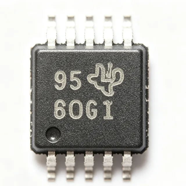
ADS1115IDGSR - 16-Bit I2C ADC with PGA | TI | Sensor Nodes
The Texas Instruments ADS1115IDGSR is a precision, low-power, 16-bit delta-sigma analog-to-digital converter (ADC) with an I2C-compatible interface, supplied in a 10-pin VSSOP (DGS) package. It integrates a programmable gain amplifier (PGA), a low-drift voltage reference, an internal oscillator, and a digital comparator, enabling compact high-resolution measurement systems with minimal external components. An analog-to-digital converter (ADC) is a mixed-signal device that translates continuous analog voltages into discrete digital codes that microcontrollers and processors can interpret. The ADS1115 operates as a sigma-delta ADC, using oversampling and noise shaping to achieve 16-bit resolution at conversion rates up to 860 samples per second (SPS). Within the signal-chain hierarchy, it belongs to precision data-acquisition ICs and eliminates the need for an external reference or clock source. Key features include four single-ended or two differential input channels via an input multiplexer, a PGA with gains from 2/3 to 16 V/V, an I2C interface supporting four bus addresses (0x48 through 0x4B), and an onboard comparator with ALERT/conversion-ready output. The device operates from a 2.0V to 5.5V supply over -40C to +125C, drawing only about 150 uA of supply current in continuous mode. The ADS111x architecture uses a delta-sigma modulator followed by a digital decimation filter for high accuracy at low power. The integrated PGA amplifies small sensor signals before conversion to improve effective resolution, while the low-drift internal reference keeps industrial measurements stable over time and temperature. The lead-free VSSOP-10 package (3.00mm width) suits space-constrained PCB layouts. Typical applications include battery voltage and current monitoring, portable instrumentation, IoT sensor nodes, temperature and pressure measurement, and industrial process control. Because no external reference or oscillator is required, the ADS1115IDGSR reduces BOM complexity in designs needing 16-bit accuracy on an I2C bus. For best performance, place a 0.1uF decoupling capacitor close to VDD and use the ADDR pin to avoid I2C bus conflicts. Keep source impedance low enough to charge the sampling capacitor; a low-noise LDO such as TPS7A26-Q1 further improves measurement stability.

ADS1115IDGSR-Q1 - 16-Bit I2C ADC, 860SPS | Texas Instruments
The Texas Instruments ADS1115IDGSR-Q1 is a precision, low-power, 16-bit, I2C-compatible delta-sigma analog-to-digital converter (ADC) in a 10-pin VSSOP (DGS) package, qualified to AEC-Q100 for automotive applications. It integrates a 4-channel input multiplexer, a programmable gain amplifier (PGA), a low-drift internal voltage reference, an internal oscillator, and a digital comparator, enabling compact single-chip signal acquisition. An ADC (analog-to-digital converter) is a mixed-signal device that converts continuous analog voltages into discrete digital values. Within the converter hierarchy, the ADS1115 is a delta-sigma (over-sampling) ADC, a topology prized for high resolution and low noise at modest sample rates, sitting above SAR ADCs in resolution and below integrating ADCs in speed. It connects to any host MCU or processor via an I2C bus, making it a power-management and sensor-measurement building block. Key features include 16-bit resolution with up to 860 samples per second (SPS) conversion rate, an I2C interface supporting four selectable addresses, and a PGA with gain settings that allow full-scale ranges down to the +/-256 mV range for direct connection of small signals. The integrated digital comparator supports alert-based operation, reducing host polling overhead. Conversion rate and duty cycling support low average power consumption in battery-backed systems. The delta-sigma architecture oversamples the input and applies digital decimation filtering, yielding excellent linearity and noise performance without external precision components. Because reference, oscillator, and PGA are on-chip, external BOM count stays minimal and channel-to-channel measurements remain consistent. Typical applications include automotive battery-voltage and current monitoring, sensor measurement in body and chassis modules, battery management systems (BMS) auxiliary sensing, factory automation analog input modules, and precision portable instrumentation. The Q1 qualification makes it a natural fit alongside TI automotive power and monitoring devices. Design tip: the input pins must not exceed VDD + 0.3V; for measuring rails above the supply, use a resistive divider and match the source impedance to the PGA input requirements to preserve accuracy.

ADS1118IDGSR - 16-Bit 860-SPS 4-Channel ADC | TI
The Texas Instruments ADS1118IDGSR is a 16-bit, 860-SPS, 4-channel delta-sigma analog-to-digital converter with a programmable gain amplifier, integrated voltage reference, oscillator, temperature sensor, and SPI interface, housed in a 10-VSSOP package. It is designed for low-power precision measurement systems and supports analog sensor inputs as well as temperature sensing. An ADC converts continuous analog voltage into a numeric value for processing, measurement, or control. The ADS1118 belongs to the delta-sigma ADC class, where an internal modulator and digital filter shape the conversion result. Its integrated PGA allows low-level sensor signals to be amplified before conversion, while the internal reference, oscillator, and temperature sensor reduce the number of external support components required in compact measurement designs. The main headline specifications are 16-bit resolution, conversion rates up to 860 samples per second, four analog input channels, and operation across a -40°C to +125°C temperature range. The device supports SPI-compatible serial communication and is offered in a small 10-pin VSSOP package. The integrated reference and temperature sensor are especially useful for sensor measurements, thermocouple-related monitoring, and systems requiring a compact analog front end. The delta-sigma architecture provides high resolution for low-frequency and slowly changing signals, while the programmable gain amplifier supports a range of input amplitudes. The internal oscillator allows operation without an external clock, which can simplify PCB design and reduce component count. The ADC is suitable when deterministic digital readout, modest conversion speed, and low power consumption are more important than very high sample rates. Typical applications include industrial process monitoring, temperature sensing, pressure and strain-signal acquisition, portable instrumentation, environmental measurement, and low-power embedded sensing. The integrated temperature sensor can provide a local temperature reading, while the analog channels support external sensors such as thermistors, resistive bridges, potentiometers, and other slowly varying analog sources. A key design consideration is analog signal conditioning and PCB layout. The sensor input must stay within the ADC input range, and the PGA gain must be selected so that the conditioned signal uses the converter’s available resolution without overloading the input. Decoupling capacitors should be placed close to the power pins, and the analog and digital return paths should be arranged to minimize noise coupling into the measurement channels. The 860-SPS maximum rate also means that applications requiring faster sampling need a different ADC architecture. This page combines the manufacturer’s published ADS1118 features, distributor pricing and availability signals, package information, application guidance, and drop-in replacement analysis for engineers evaluating the ADS1118IDGSR.

ADS1118QDGSRQ1 - 16-bit 860SPS Automotive Delta-Sigma ADC | TI
The Texas Instruments ADS1118QDGSRQ1 is an automotive-qualified, precision, low-power, 16-bit, 860-SPS, 4-channel, delta-sigma analog-to-digital converter (ADC) that integrates a programmable gain amplifier (PGA), voltage reference, internal oscillator, high-accuracy temperature sensor, and an SPI-compatible serial interface in a 10-pin VSSOP (DGS) package. It provides 4 single-ended or 2 differential input channels, supports a wide 2.0 V to 5.5 V analog supply range, and delivers up to 16 bits of effective resolution across data rates from 8 SPS to 860 SPS, with an integrated PGA offering gains of 1, 2, 4, 8, 16, 32, 64, and 128 to accommodate low-level sensor signals. A delta-sigma ADC is a type of oversampling converter that uses noise shaping and digital filtering to achieve high resolution and excellent noise rejection at low frequencies. In the broader taxonomy it sits under: ADC -> data converter -> signal chain IC -> mixed-signal semiconductor. The ADS1118-Q1 is the automotive (-Q1) variant of the industrial ADS1118 family, designed for AEC-Q100 qualified applications where robust thermal, EMI, and reliability performance is mandatory. Key features include an integrated low-drift voltage reference (typically 4.096 V with 0.01 %/°C drift), an on-chip temperature sensor with 0.5 °C typical accuracy, a low quiescent current of typically 150 µA in continuous-conversion mode, and a power-down current below 1 µA. The internal PGA eliminates the requirement for an external instrumentation front-end in many bridge sensor applications. The SPI-compatible interface supports up to 4-wire connections and allows daisy-chaining of multiple devices. Typical applications include automotive sensor monitoring (battery management systems, cabin climate, occupant detection), industrial process control (4-20 mA loop digitization, RTD/thermocouple digitization), portable instrumentation, and temperature-compensated measurement chains. The wide supply range and small footprint make it ideal for space-constrained designs. When designing with this device, place the supply decoupling capacitor within 5 mm of the AVDD pin and keep digital traces away from analog inputs. The -Q1 suffix guarantees operation from -40 °C to +125 °C and AEC-Q100 Grade 1 qualification for automotive use cases.

ADS114S08BIPBSR - 16-Bit 4kSPS 12-Ch Delta-Sigma ADC | TI
The Texas Instruments ADS114S08BIPBSR is a 16-bit, 4-kSPS, 12-channel delta-sigma (ΔΣ) analog-to-digital converter with an integrated programmable gain amplifier (PGA) and voltage reference, supplied in a 32-pin TQFP (PBS) package measuring 5x5 mm. It is optimized for low-cost sensor measurement applications and consumes as little as 280 µA of supply current, which makes it appropriate for battery-powered or thermally constrained systems. The integrated PGA accepts gains from 1 to 128 V/V, allowing direct interface to low-output sensors such as load cells, thermocouples, and bridge-type pressure transducers without external amplification. A delta-sigma ADC is a noise-shaping converter that oversamples the analog input at a rate many times higher than the Nyquist frequency of the output data rate, then shapes quantization noise out of the baseband and decimates the bitstream to produce a high-resolution result. Within the broader data-converter hierarchy, the ADS114S08B occupies the precision-low-speed node between successive-approximation register (SAR) ADCs and wider-bandwidth delta-sigma parts, positioning it as a power management and signal-chain IC for measurement-grade instrumentation. Key specifications include a maximum data rate of 4 kSPS, simultaneous 50 Hz / 60 Hz line-frequency rejection at data rates of 20 SPS or lower, a low-latency digital filter, on-chip temperature sensor, and an SPI-compatible serial interface. The internal voltage reference is selectable between an internal 2.5 V source and an external reference, supporting ratiometric and absolute measurement topologies. Twelve analog input channels can be configured as differential, pseudo-differential, or single-ended, providing flexibility for multi-sensor designs. The device architecture pairs a chopper-stabilized input front end with a second-order delta-sigma modulator and a programmable SINC3 digital filter. Chopper stabilization reduces the 1/f noise corner and corrects input-offset drift over temperature, while the SINC3 filter gives first-cycle conversion latency at low data rates, useful for closed-loop control applications. The internal PGA gain of up to 128 V/V combined with the low input-referred noise allows the ADC to resolve microvolt-level signals directly. Typical applications include weigh scales, strain-gauge bridge sensors, thermocouple temperature measurement, RTD signal conditioning, industrial process-control analog input modules, and portable medical instrumentation such as blood-pressure monitors and body-composition analyzers. The wide analog supply range of 2.7 V to 5.25 V and digital supply range of 2.7 V to 3.6 V let it pair directly with 3.3 V MCUs and 5 V analog signal chains. When designing with this ADC, evaluate total input-referred noise against the target data rate because the SINC3 filter trades bandwidth for resolution - selecting a 2.5 SPS or 20 SPS output rate improves effective resolution to 16-bit noise-free codes for weigh-scale applications. Decouple AVDD and DVDD with 1 µF and 100 nF ceramic capacitors placed within 2 mm of the supply pins to keep digital switching noise out of the modulator. This page synthesizes distributor pricing, same-brand drop-in alternatives, and practical design notes not found in the standalone manufacturer datasheet, providing engineers with a single reference for selection, replacement, and PCB layout decisions.

ADS114S08BIRHBR - 16-bit 4kSPS 12-ch Delta-Sigma ADC | Texas Instruments
The Texas Instruments ADS114S08BIRHBR is a 16-bit, 4-kSPS, 12-channel, delta-sigma analog-to-digital converter with integrated PGA and 2.5 V voltage reference, housed in a 32-pin VQFN (RHB) 5x5 mm package with exposed thermal pad. It delivers 16-bit resolution at up to 4 kSPS data rate, consumes as little as 280 µA, and provides programmable gain from 1 to 128. A delta-sigma ADC is a type of analog-to-digital converter that uses oversampling and noise shaping to achieve high resolution at low sample rates. Delta-sigma ADCs are a subset of integrating ADCs, which fall under the broader category of data converters, mixed-signal ICs, and finally semiconductors. The ADS114S08B sits in this taxonomy between precision SAR ADCs (single-shot, medium speed) and wideband pipeline ADCs (high speed, lower resolution). Delta-sigma converters dominate low-frequency precision measurement - sensor signal conditioning, weigh scales, temperature, strain gauge bridges - because their noise-shaping topology yields 16-24 effective bits at bandwidths below a few kHz. Key features include 12 analog input channels with low-noise PGA gains of 1, 2, 4, 8, 16, 32, 64, and 128, programmable data rates from 2.5 SPS to 4 kSPS, simultaneous 50-Hz and 60-Hz line rejection at data rates up to 20 SPS, an integrated 2.5 V low-drift voltage reference, and two matched excitation current sources for RTD and bridge sensor biasing. The device offers low-latency digital filter response, an SPI-compatible serial data interface, and an operating supply current as low as 280 µA in low-power mode. Architecture-wise, the ADS114S08B uses a 2nd-order delta-sigma modulator followed by a programmable SINC + FIR digital decimation filter. The modulator clock is derived from an internal oscillator; the digital filter provides both single-cycle and FIR modes. The integrated PGA delivers gains up to 128 V/V, allowing direct interface to thermocouples and strain-gauge bridges without external instrumentation amplifiers. The integrated low-drift 2.5 V reference eliminates an external reference IC for cost-sensitive designs. Typical applications include weigh scales and load cell digitizers, RTD and thermocouple temperature acquisition, strain-gauge bridge measurement, industrial process control analog input modules, factory automation sensor interfaces, and battery-powered portable sensor instruments. The 280 µA quiescent current makes it well suited for battery-powered or loop-powered 4-20 mA sensor transmitters where total analog-section power budget is constrained. When designing with the ADS114S08B, allocate GPIO on the host microcontroller for /DRDY, /CS, SCLK, DIN, DOUT/DRDY, and /RESET. Use a clean low-noise analog supply with a ferrite bead separating it from the digital 3.3 V rail. Place the 0.10 µF + 10 µF decoupling pair within 5 mm of the AVDD pin. The exposed thermal pad (pin 33) must be soldered to a continuous analog ground plane for thermal and EMI performance.

ADS1201U - 24-Bit 1 kSPS Delta-Sigma ADC | Texas Instruments
The Texas Instruments ADS1201U is a 24-bit high-dynamic-range delta-sigma modulator with a fully differential input, 1 kSPS conversion rate, and two-wire serial interface in a 16-pin SOIC package. It supports internal or external voltage references and includes on-chip switches for calibration, making it suitable for precision analog measurement systems requiring high dynamic range and low-noise signal acquisition. A delta-sigma ADC is a signal-conversion IC that uses oversampling, noise shaping, and digital filtering to convert an analog input into a high-resolution digital result. Within the ADC hierarchy, the ADS1201U belongs to the delta-sigma modulator family, provides analog-to-digital conversion, and ultimately functions as a precision data-conversion IC. Its fully differential architecture is particularly useful when the source has a small voltage across a common-mode range and benefits from rejection of common-mode noise. Key features include a nominal 24-bit resolution, a 1 kSPS data rate, and approximately 130 dB of dynamic range. The two-wire interface reduces the number of serial connections required between the converter and a controller. The differential input supports single-ended or differential source arrangements when paired with suitable front-end circuitry, while selectable internal or external references allow the reference voltage to be matched to the transducer and analog signal chain. The delta-sigma architecture trades conversion speed for resolution and noise performance. It is most effective for slowly changing or precision-oriented signals rather than high-bandwidth waveform acquisition. The on-chip calibration switches support system-level calibration, and the 16-pin SOIC package permits assembly using conventional surface-mount production methods. Maximum power dissipation is reported as 40 mW, making thermal design relatively manageable in typical precision-measurement equipment. Typical uses include pressure and load-cell signal conditioning, industrial sensor acquisition, instrumentation amplifiers, weigh systems, and low-frequency measurement front ends. A controller can read the serial output and perform digital filtering or scaling as required by the measurement system. The differential input can also front-end sensor bridges where preserving signal integrity and rejecting common-mode disturbances are priorities. Designers should verify the required analog bandwidth, digital-filter settling time, reference configuration, and serial timing before fixing the system sampling strategy. Input protection, reference bypassing, and a quiet ground layout are important because they can affect achievable resolution. The 40 mW maximum power dissipation rating provides a useful starting point, but actual board-level thermal behavior should be checked against the final operating conditions. This page consolidates verified manufacturer and distributor information, lifecycle context, candidate replacements, and practical selection guidance. It also distinguishes confirmed device attributes from parameters that still require verification, helping engineers shorten datasheet review and replacement-planning time without inventing unavailable electrical details.

ADS1210P - 24-Bit Delta-Sigma ADC 16kSPS, DIP-18 | Texas Instruments
The Texas Instruments ADS1210P is a precision 24-bit delta-sigma analog-to-digital converter with 1 differential input channel, 23 bits of effective resolution at 10 Hz, and 20 bits at 1000 Hz. It provides up to 16 kSPS output data rate and is housed in an 18-pin PDIP (through-hole) package. The device operates from a single +5 V analog supply and a separate digital supply, with low noise and a programmable gain amplifier (PGA) on-chip. A delta-sigma ADC is a type of oversampling converter that achieves very high resolution by trading speed for noise averaging. The ADS1210P belongs to the precision-measurement ADC family, within the broader hierarchy: ADC -> data converter -> signal chain IC -> semiconductor. Its combination of a wide dynamic range, programmable gain, and integrated flexible serial interface (SPI/SSI-compatible with 2-wire mode) makes it suitable for instrumentation-grade front ends. Key features include: 23-bit effective resolution at 10 Hz, 20 bits at 1000 Hz, differential analog inputs, programmable gain amplifier with gain up to 128, programmable cutoff frequency, on-chip calibration, and a flexible SPI-compatible SSI interface that also supports a 2-wire mode. These features allow the ADS1210P to replace a complete discrete precision ADC front end with a single IC, simplifying high-accuracy measurement designs. Typical applications include weigh scales (load-cell digitizers), industrial process control sensors (pressure, strain, temperature via RTD/thermocouple conditioning), precision transducer readouts (e.g., weighing platforms, flow meters), and laboratory instrumentation. The internal PGA and single-cycle conversion settling make it well suited to multiplexed low-frequency, high-resolution systems. When designing with this part, observe careful grounding between the analog AVSS/AVDD pins and the digital DVSS/DVDD pins, and place the reference and input decoupling capacitors close to the package. The ADS1210/ADS1211 share a common footprint but differ on pins 1-3 and 22-24, so a layout that ties unused inputs to analog ground is needed for ADS1211 drop-in. This page synthesizes distributor pricing, drop-in alternatives, and practical design notes not found in the manufacturer datasheet.
ADS1210PG4 - 24-Bit Delta-Sigma ADC, 18-PDIP | Texas Instruments
The Texas Instruments ADS1210PG4 is a 24-bit precision delta-sigma analog-to-digital converter that operates from a single +5V supply, packaged in an 18-pin PDIP (through-hole) outline and rated for the -40C to +85C industrial temperature range. It delivers up to 16 kS/s effective sampling, supports differential bipolar/unipolar inputs, integrates a programmable gain amplifier (PGA), and exposes a serial SPI-compatible interface for microcontroller or DSP host connection. The delta-sigma modulator is followed by a digital SINC^4 decimation filter, giving 23-bit effective resolution at a 10 Hz data rate and 20-bit effective resolution up to 1 kHz, with 22 bits of no-missing-code performance. An ADC (analog-to-digital converter) is a mixed-signal integrated circuit that converts a continuous analog voltage into a discrete digital code; the delta-sigma architecture in particular uses oversampling and noise-shaping to push quantization noise away from the signal band of interest, then decimates to a lower-rate high-resolution output. The ADS1210PG4 sits in the precision data-acquisition tier, well below SAR ADCs in raw speed but well above them in noise-free resolution, making it the device of choice when measuring low-frequency transducer signals such as strain gauges, RTDs, thermocouples, and weigh-scale load cells. Key features include a differential front end with wide common-mode range, self-calibration of offset and gain, on-chip input buffers, and a flexible SINC^4 digital filter with programmable sample rates from 1 Hz to 16 kHz via an external reference and clock. The integrated PGA provides gains from 1 to 16 in binary steps, allowing small transducer signals (millivolts) to be amplified before conversion and eliminating the need for an external instrumentation amp in many designs. Calibration modes (self, system, background) compensate for drift and PC-board leakage. Typical applications include industrial weighing scales, process instrumentation (pressure, flow, temperature), smart sensor transmitters, portable medical instrumentation, and laboratory data loggers where single-supply +5V operation, high resolution, and a parallel-through-hole footprint simplify PCB and firmware design. When designing with the ADS1210PG4, treat the analog and digital grounds as split nets joined at a single point beneath the IC, place the 1 nF to 10 uF decoupling capacitors as close as possible to AVDD/DVDD pins, and drive the modulator clock with a clean low-jitter source. The 'G4' suffix denotes the Pb-free (RoHS) finish designation; the underlying silicon is identical to the legacy ADS1210P. This page synthesizes distributor pricing, drop-in same-package alternatives, and practical design notes that complement rather than duplicate the manufacturer datasheet.

ADS1210U - 24-Bit Delta-Sigma ADC | Texas Instruments
The Texas Instruments ADS1210U is a 24-bit precision delta-sigma analog-to-digital converter designed for low-level differential measurements, with a programmable gain amplifier, differential inputs, and an SPI-compatible serial interface supporting two-wire mode. The converter operates from a single +5 V supply and is available in an 8-SOIC package according to the supplied distributor data. An ADC is a semiconductor that converts an analog voltage into a digital number. Within the hierarchy of signal-chain components, the ADS1210U is a delta-sigma ADC, a precision ADC architecture used for high-resolution measurement. It sits between sensors or transducers and a digital controller, where it captures small voltage differences while rejecting common-mode noise through differential sampling. The ADS1210U provides up to 24-bit nominal resolution, 23 effective bits at a 10 Hz data rate, and 20 effective bits at 1000 Hz. Its programmable gain amplifier accommodates low-level sensor signals, while programmable cutoff frequencies allow the digital filter bandwidth to be matched to the measurement. The flexible SPI-compatible SSI interface supports conventional serial control and a two-wire mode for systems with limited connector pins. Internally, the ADS1210 uses a delta-sigma conversion architecture to achieve wide dynamic range and high linearity. The manufacturer describes the ADS1210 family as providing 22 bits of no-missing-code performance. Resolution alone should not be confused with useful measurement accuracy: effective resolution declines as the data rate increases because the converter trades noise performance for faster conversions. Filter settings, input noise, reference voltage, source impedance, and PCB layout therefore determine practical measurement resolution. Typical uses include bridge sensors, pressure and load-cell transducers, industrial instrumentation, low-level voltage acquisition, and embedded systems that require differential measurement with programmable gain. The differential input structure is particularly useful when the wanted signal is small relative to system noise or when the sensor is not referenced to the converter ground. For reliable operation, follow the manufacturer datasheet for input and reference decoupling, grounding, digital-interface timing, and analog-layout recommendations. Place the analog input and reference paths away from noisy switching nodes, provide local high-frequency bypass capacitance, and use a stable reference source when accurate ratio-independent results are required. This page combines the supplied manufacturer and distributor information with lifecycle, interface, selection, and design guidance. It also distinguishes verified drop-in interchangeability from related converters that cannot replace the ADS1210U without footprint, pin, or measurement-system changes.

ADS1211 - 24-Bit Delta-Sigma ADC, 4-Channel | Texas Instruments
The Texas Instruments ADS1211 is a precision, wide dynamic range, delta-sigma analog-to-digital converter (ADC) with 24-bit resolution, operating from a single +5V supply. It features a 4-channel input multiplexer and is available in 24-pin DIP, 24-lead SOIC, and 28-lead SSOP packages, targeting high-resolution measurement in smart transmitters, industrial process control, weigh scales, chromatography, and portable instrumentation. A delta-sigma ADC is a type of analog-to-digital converter that uses oversampling and noise shaping to achieve very high resolution, typically 16 to 24 bits. It is ideal for low-frequency, high-precision measurement where accuracy matters more than conversion speed. The ADS1211 belongs to the precision delta-sigma ADC family within the broader data-converter hierarchy, bridging analog sensors and digital processing systems. Key features include 24-bit resolution (23 bits effective at 10 Hz output rate, 20 bits effective at 1000 Hz), differential inputs, a programmable gain amplifier (PGA), and a programmable digital filter cut-off frequency. The flexible synchronous serial interface is SPI compatible and offers a two-wire control mode for low-cost isolation. Self-calibration ensures accuracy over time and temperature. Architecturally, the ADS1211 combines a delta-sigma modulator with an on-chip digital filter, producing high-resolution results from a single +5V supply at approximately 12mW power dissipation, suiting portable and battery-powered designs. The VBIAS reference-bias output supports biased sensors such as bridge transducers. Typical applications include smart transmitters, industrial process control, weigh scales, and chromatography instruments. The integrated 4-channel multiplexer lets multiple sensors share one ADC, cutting system cost and board area. When designing with the ADS1211, decouple analog and digital supplies carefully, use a low-noise stable reference to realize full 24-bit performance, and configure SPI timing to match the host microcontroller. Prices as of 2026-08-30; verify current distributor stock.

ADS1211E - 24-Bit 4-Input Delta-Sigma ADC | Texas Instruments
The Texas Instruments ADS1211E is a 24-bit delta-sigma analog-to-digital converter with four single-ended inputs, a programmable gain amplifier, an internal voltage reference, and a maximum data rate of 15.6 kSPS. The device operates from a single +5 V supply and is supplied in a 28-pin SSOP package rated for industrial temperature applications. A delta-sigma analog-to-digital converter is a signal-conversion device that oversamples its input and uses digital filtering and noise shaping to provide high resolution with good rejection of out-of-band noise. The ADS1211 belongs to the broader ADC hierarchy: analog-to-digital converter -> delta-sigma ADC -> precision data-converter IC. Its differential-input architecture is designed for low-level sensor signals, bridge transmitters, and industrial measurement systems where dynamic range and noise performance are more important than maximum conversion speed. Key features include 24-bit conversion resolution, four analog input channels, a 1.7 to 5.5 V nominal supply range as identified by the manufacturer family documentation, an internal reference, and selectable PGA gain. The product-page description identifies the ADS1211 family as an eight-channel delta-sigma ADC, while distributor and package data identify the ADS1211E configuration as a four-input device in a 28-pin SSOP. These different operating modes should be confirmed against the exact channel-configuration table in the manufacturer datasheet before layout is released. The single-converter delta-sigma architecture provides a programmable-gain front end and continuous internal offset and gain calibration functions. These features make the device suitable for precision acquisition systems in which sensor drift, amplifier offset, and reference stability influence overall measurement accuracy. The digital interface supports device configuration, data retrieval, and calibration commands through a serial control interface. Typical uses include industrial pressure and temperature acquisition, load-cell and strain-gauge measurement, current-sensing instrumentation, and low-level process-control monitoring. For battery-operated or isolated systems, the relatively low data rate of 15.6 kSPS allows more time for conversion, filtering, and low-power duty-cycling than a high-speed SAR ADC would permit. Design should begin by confirming the analog input range, PGA gain, supply tolerance, reference configuration, and digital-interface levels against the datasheet. Place the reference and analog-supply bypass capacitors close to their pins, route analog inputs away from high-current switching paths, and treat the exposed analog-ground and digital-ground connections according to the recommended layout in the manufacturer documentation. This page consolidates manufacturer specifications, distributor package and pricing information, verified orderable variants, and practical selection guidance. It also distinguishes documented drop-in device options from functionally similar but non-pin-compatible ADC families, preventing a footprint change from being mistaken for a true drop-in replacement.