IC giao tiếp
Danh mục con
Sản phẩm (2.300+)

ASM2464PDX - USB4/TB to PCIe Gen4 x4 NVMe Bridge | ASMedia
The ASMedia ASM2464PDX is a USB4/Thunderbolt to PCIe/NVMe accessory bridge controller delivering 40 Gbps over USB4/Thunderbolt and tunneling PCIe Gen4 x4 to NVMe SSDs or general PCIe devices, housed in a compact RoHS-green BGA package (FCCSP-273, 10x10 mm class per distributor listings). A bridge controller is a protocol-conversion IC that sits between a host interface and a device interface, translating one bus protocol into another. In the USB4 ecosystem, bridge controllers let legacy protocols such as PCI Express ride inside the USB4/Thunderbolt fabric, where USB4 router-to-router tunnels carry PCIe and USB transactions transparently across the domain. Within the power-management-and-connectivity hierarchy of a host system, the ASM2464PDX functions as the device-side endpoint router of a USB4/Thunderbolt daisy chain. Key features include in-house designed ASMedia USB4/Thunderbolt PHYs, native PCIe Gen4 x4 downstream connectivity for maximum NVMe throughput, and support for USB4, Thunderbolt 3, and USB 3.x legacy host operation. The PDX variant specifically targets general PCIe devices in addition to NVMe SSDs, making it the ASMedia part of choice for Thunderbolt/USB4 eGPU docks and expansion enclosures. Technically, the ASM2464PDX integrates the USB4/Thunderbolt Gen3 x2 PHY and the PCI Express Gen4 PHY with VDD, VCCL, and VCCH voltage domains. It is clocked from a local 25 MHz crystal, supports multiple GPIO pins for platform customization, and integrates the protocol routers needed to encapsulate PCIe and USB traffic into USB4 tunneling. Typical applications include USB4/Thunderbolt NVMe SSD enclosures, Thunderbolt eGPU adapters, PCIe accessory expansion docks, and high-speed developer/debug hardware that exposes general PCIe lanes over a single USB-C cable. Design consideration: the PDX suffix denotes an improved variant of the ASM2464PD focused on power-delivery stability and reduced thermal throttling under sustained high-bandwidth loads such as eGPU traffic; board designs should still provide solid VCCL power planes and thermal relief for sustained Gen4 x4 transfers. This page synthesizes distributor availability, the documented PD-vs-PDX differences, competitor context (Intel JHL7440/JHL9480), and practical design notes not found in the manufacturer datasheet.

ASM58048 - 48-Lane 16-Port PCIe 4.0 Switch | ASMedia Technology
The ASMedia Technology ASM58048 is a 48-lane, 16-port PCIe Packet Switch fabricating a high-speed PCI Express interconnect switching fabric for AI, server, storage, and workstation platforms. First showcased at COMPUTEX 2025 and sampled in Q3 2025, it belongs to ASMedia's PCIe packet switch roadmap covering all PCIe generations with a product line ranging from 3 to 80 lanes. According to the PCI-SIG integrator listing, the ASM58048 identifier is registered as a 48-lane, 16-port PCIe Switch function. A PCIe packet switch is a switching fabric device that sits in the PCI Express hierarchy between a host root complex and multiple endpoints. It performs store-and-forward or cut-through packet routing of TLPs (Transaction Layer Packets), enabling one upstream port to fan out to several downstream ports. In the system hierarchy, the device spans PCIe switch -> interconnect fabric -> host interface -> high-speed serial interface -> semiconductor. Key characteristics include 48 lanes of PCIe connectivity and 16 configurable ports, giving system architects flexible bifurcation options for connecting multiple NVMe SSDs, GPUs, or network adapters to a limited number of host CPU lanes. ASMedia states that full compatibility and performance comparable to international competitors were design targets, and that the device's own fully verified PHY technology underpins the silicon. The architecture leverages ASMedia's in-house PHY IP, and the follow-on PCIe Gen5 product with independently verified PHY is nearing design finalization, indicating the ASM58048 targets the PCIe Gen4 class of interconnect workloads. Typical applications include NAS high-speed cache acceleration - per ASMedia's CES 2026 announcement, the ASM58048 enables multiple high-speed NVMe SSDs to be connected at the NAS front end forming a high-speed cache tier for AI data preprocessing - plus AI workstation GPU expansion, server storage backplanes, and add-in-card fan-out designs. When designing with this device, confirm lane allocation and bifurcation settings against your board's power and reference-clock topology, and validate link training across all 16 ports in system-level bring-up. This page synthesizes PCI-SIG registration data, manufacturer press releases, and drop-in replacement guidance not found in distributor listings.

AT97SC3205T-U3A17-AA - TPM I2C Security Module | Microchip
The Microchip AT97SC3205T-U3A17-AA is a fully integrated Trusted Platform Module (TPM) security IC designed to be embedded into computer and embedded systems for hardware-rooted cryptographic functions. Housed in a 28-pin SSOP package, this device conforms to the Trusted Computing Group (TCG) Trusted Platform Module Main v1.2, r116 specification and is intended for I2C-compliant host integration, providing secure key storage, platform authentication, and integrity measurement. What is a TPM? A Trusted Platform Module is a dedicated hardware security controller that provides tamper-resistant storage for cryptographic keys, secure generation of RSA keys up to 2048 bits, platform integrity measurement via SHA-1/SHA-256, and remote attestation. The TPM sits on the I2C bus as a peripheral to the host CPU and occupies a unique position in the security hierarchy: hardware root of trust -> security module -> platform security -> system integrity. AT97SC3205T-U3A17-AA implements this hierarchy in a single low-power CMOS device. Key features of the AT97SC3205T-U3A17-AA include RSA key generation up to 2048-bit keys, SHA-1 and SHA-256 hash engines for platform integrity, hardware random number generator, secure key storage with hardware tamper detection, I2C host interface for low-pin-count integration, and an integrated firmware that is field-upgradable through a secured loader. The device operates from a single 3.3V supply and uses CMOS technology for low quiescent current. The AT97SC3205T family is positioned for desktops, laptops, embedded industrial PCs, and other systems that require TCG 1.2 compliance (note: not TCG 2.0). Designers select this part when TCG Main v1.2 r116 compliance is mandated by procurement specifications, by Microsoft Windows Vista/7 era certification requirements, or by embedded OEMs whose customers require TPM presence in the BOM. Because TPM 2.0 has largely replaced 1.2 in new designs, this part serves legacy systems, industrial security appliances, and embedded markets where long-life TCG 1.2 platforms are standard. Typical applications include commercial desktop and laptop motherboards, industrial PCs and HMIs, point-of-sale terminals, secure printing devices, and embedded security appliances. The I2C interface allows integration with both x86 chipsets and ARM-based SoCs that expose I2C. For TCG 2.0 systems, consider AT97SC3205T family members with TCG 2.0 compliance or the newer AT97SC3205 family variants. When designing with the AT97SC3205T-U3A17-AA, the host driver stack must match the TCG 1.2 specification; Linux drivers (tpm_tis_i2c) and Windows TBS (TPM Base Services) provide the OS-level interface. The I2C lines require pull-up resistors per I2C specification, and the TPM's GPIO/PIR (presence) pin must be wired to the platform's TPM-presence detection logic. Power sequencing: VCC must stabilize before the host begins I2C transactions. This page synthesizes distributor availability, parametric alternatives within the same SSOP-28 footprint, and platform-integration design notes drawn from manufacturer reference documentation - content not found in the standalone datasheet.

ATA6563-GAQW1 - High-Speed CAN FD Transceiver SOIC-8 | Microchip
The Microchip ATA6563-GAQW1 is a high-speed CAN FD transceiver providing an interface between a CAN protocol controller and the physical two-wire CAN bus. Housed in an 8-pin SOIC package, the device supports CAN FD data rates up to 5 Mbit/s and operates from a 5V nominal supply across an ambient temperature range of -40C to +150C (AEC-Q100 Grade 0). The integrated VIO pin and Wake-Up Pattern (WUP) function provide low-power standby capability with bus wake-up, enabling nodes to remain quiescent while still monitoring the CAN bus. A CAN FD transceiver (Controller Area Network with Flexible Data-Rate) is the physical-layer device that translates the differential logic signals of a CAN protocol controller into the bus-side differential signaling required by the ISO 11898-1 standard. CAN transceivers belong to the broader category of automotive-grade communication interface ICs, sitting in the signal chain between a microcontroller's CAN controller and the actual bus wiring. CAN FD extends classical CAN from 1 Mbit/s to 5 Mbit/s by allowing faster bit rates during the data phase, and the transceiver must preserve the dominant-bit timing needed for arbitration. Key features include compliance with ISO 11898-1:2015, low electromagnetic emission (EME), high electromagnetic immunity (EMI), an under-voltage detection on VCC and VIO, thermal shutdown protection, and bus-pin transient voltage robustness typical of automotive transceivers. The -GAQW1 ordering code designates the SOIC-8 variant (3.9 mm body width, tape-and-reel packaging, automotive qualification per AEC-Q100). The architecture combines a differential transmitter with slope-controlled output to limit EME, a high-CMRR differential receiver, and integrated protection diodes on the bus pins. The VIO reference pin lets the logic interface track I/O voltages down to 1.8V on modern microcontrollers, while the WUP function filters remote-frame wake-up events per the ISO 11898-2 standard. Bus pins are tolerant to -27V to +40V and include load-dump resilience typical of automotive CAN transceivers. Typical applications include automotive body and powertrain ECUs, ADAS sensor nodes, industrial CAN FD networks, gateway modules bridging CAN and CAN FD segments, and battery-management or motor-control ECUs that need a low-power standby mode with selective wake-up. Industrial uses include CANopen and DeviceNet nodes and remote I/O blocks. When designing with the ATA6563-GAQW1, place a 100 nF decoupling capacitor close to VCC and use a split termination (60 ohm resistor + 4.7 nF capacitor) on each bus terminal to meet OEM EMC requirements. This page synthesizes distributor pricing, drop-in alternatives, and practical design notes not found in the manufacturer datasheet, giving engineers an at-a-glance view of availability, cross-brand equivalents, and CAN bus design best practices.
ATA6571RT - Radiation-Tolerant CAN FD Transceiver, 5 Mbps | Microchip
The Microchip Technology ATA6571RT is a radiation-tolerant, stand-alone high-speed CAN FD transceiver that interfaces a Controller Area Network (CAN) protocol controller and the physical two-wire CAN bus. The device supports data rates up to 5 Mbps in CAN FD mode, operates from a 4.5V to 5.5V supply, and is delivered in a small-footprint SOIC-style package suited to flight hardware. A CAN transceiver is the physical-layer bridge between a microcontroller's CAN protocol controller and the differential two-wire bus. In modern in-vehicle networks (IVN), CAN FD (Flexible Data-rate) extends classic CAN's 1 Mbps ceiling by allowing higher bit rates in the data phase, which is critical for advanced driver-assistance (ADAS) sensors, body controllers and powertrain ECUs. The ATA6571RT is part of the radiation-tolerant (Rad-Tol) product family designed for low-earth-orbit constellations, GEO communications payloads and other space-grade platforms where single-event effects (SEE) and total ionizing dose (TID) must be characterized. Key features include ISO 11898-2 and ISO 11898-5 physical-layer compliance, SAE J2962-2 conformance for radiated/conducted immunity, ±40V bus fault protection, thermal shutdown, and an integrated dominant-timeout watchdog. The bus pins are designed for high DC load-dump resilience and meet the rigorous EMC/ESD requirements common to aerospace and heavy-industrial environments. Architecturally, the device combines a low-EMI driver stage with a wide-bandwidth receiver optimized for the 5 Mbps FD data phase. The radiation-tolerance is achieved through silicon process selection, characterized SEE/TID performance, and per-lot qualification testing documented in the Microchip radiation reports. Typical applications include satellite command/telemetry buses, spacecraft avionics networks, launch-vehicle data acquisition, and radiation-prone industrial controls. The same part can also be designed into high-reliability ground systems where a Rad-Tol part number simplifies parts-control and derating documentation. Design consideration: verify bus termination (typically 120 ohm at each end of the bus), place the device close to the bus connector to minimize stub length, and ensure the VCC pin has a 100 nF + 4.7 uF decoupling network within 5 mm. In space applications, single-event functional interrupt (SEFI) recovery timing must be evaluated against the host MCU's CAN controller timeout window. This page synthesizes distributor availability, drop-in Rad-Tol and standard CAN FD alternatives, and application guidance not collected in the manufacturer brochure alone.

ATECC608B-MAHCZ-S - ECC Secure Element SWI UDFN-8 | Microchip
The Microchip Technology ATECC608B-MAHCZ-S is a CryptoAuthentication cryptographic secure element (authentication IC) with ECC/ECDH hardware crypto acceleration, single-wire interface (SWI) communication, and secure hardware-based key storage, housed in an 8-pin UDFN (2x3 mm) surface-mount package. Pricing starts from approximately $1.17 per unit as of 2026-10-12 (LCSC). A secure element is a dedicated cryptographic co-processor that stores secret keys in tamper-resistant hardware, isolated from the main MCU or MPU. Within the power management and system-security hierarchy, it sits alongside microcontrollers and interface ICs, offloading asymmetric cryptography, secure boot validation, and anti-cloning duties that would otherwise expose keys in software. The ATECC608B belongs to Microchip's CryptoAuthentication family, which spans the ATECC508A, ATECC608A, and ATECC608B generations. Key features include NIST-standard P-256 elliptic-curve support for ECDSA sign/verify and ECDH key agreement, hardware SHA-256 hashing and HMAC, up to 16 configurable key storage slots, and an EUI-48/EUI-64 based serial number for device identity. The MAHCZ suffix denotes the SWI (single-wire) communication interface, requiring only a single GPIO pin over a wide voltage range. Technical depth: the device consumes extremely low power, making it well suited to battery-powered IoT endpoints. Its secure hardware key storage prevents key extraction even under sophisticated physical attacks. The ATECC608B provides security enhancements over the ATECC608A while remaining fully backwards compatible in commands, packages, and pinout, per Microchip's migration application note DS40002237A. Typical applications include IoT network endpoint authentication, secure boot firmware validation, anti-cloning protection for consumables and peripherals, and TLS client certificate storage for cloud connectivity in smart-home and industrial devices. Design consideration: choose the MAHCZ (SWI) variant only when a single-GPIO bus is required; the MAHDA variant supports standard I2C up to 1 Mbps. Reserve a GPIO on your MCU for SWI communication and plan provisioning during manufacturing. This page synthesizes distributor pricing, drop-in alternatives, pinout, and practical design notes not found in the manufacturer datasheet, providing unique cross-reference value for engineers and buyers.
ATECC608B-SSHDA-B - CryptoAuthentication IC, I2C, 8-SOIC | Microchip
The Microchip Technology ATECC608B-SSHDA-B is a member of the CryptoAuthentication family of high-security cryptographic devices that combine hardware-based key storage with hardware cryptographic accelerators. Housed in an 8-pin SOIC (3.90 mm) package, it integrates an ECC-P256 engine supporting ECDH and ECDSA, an AES-128 hardware accelerator, SHA-256 hashing, and a hardware random number generator. The device communicates with a host MCU over I2C at up to 1 Mb/s and operates from a 2.0 V to 5.5 V supply across the -40 °C to +85 °C industrial temperature range. A cryptographic co-processor is a dedicated hardware block that offloads mathematically intensive security operations from a microcontroller, isolating private keys inside a tamper-resistant silicon boundary so they never appear in host memory. Within the system hierarchy, the ATECC608B sits at the secure-element layer above general-purpose MCUs, complementing TLS software stacks with hardware root-of-trust primitives. Microchip's CryptoAuthLib software library abstracts I2C transactions so designers can issue sign/verify, key agreement, and AES-GCM commands with a few function calls. Key features include protected storage for up to 16 keys/certificates/data slots, FIPS186-3 ECDSA sign/verify at P-256, NIST SP800-56A ECDH key agreement, AES-128-GCM/ECB encryption/decryption, monotonic counters, and secure boot validation hooks. Each slot has configurable access permissions and can be locked permanently, making the device a turnkey root-of-trust for IoT endpoint authentication, anti-counterfeiting, and IP protection. The internal architecture pairs a secure EEPROM key store with hardware accelerators for ECDSA, ECDH, AES-128, and SHA-256, all fronted by a true random number generator (TRNG) that meets NIST SP800-22 guidelines. Internal voltage and tamper monitors can zeroize keys on detected glitches, while GPIO with optional secure signal assertions enable host MCU wake-up or LED feedback during provisioning. Typical applications include IoT node authentication, secure boot validation for Linux/MCU firmware, accessory and consumable anti-cloning, TLS handshake acceleration, message encryption with AES-GCM, and IP/feature enablement for licensed products. Designers add the ATECC608B to existing designs via a 2-wire I2C bus, requiring only VCC, GND, SDA, and SCL pull-ups. When designing with this device, allocate a unique 7-bit I2C address (factory default is 0x60) and respect the GPIO default-state behavior at power-up. Use Microchip's CryptoAuthLib and the AT88CK590 kit for provisioning and follow the migration guide AN5078 if upgrading from ATECC608A.
ATECC608B-SSHDA-T - CryptoAuthentication IC, SOIC-8 | Microchip
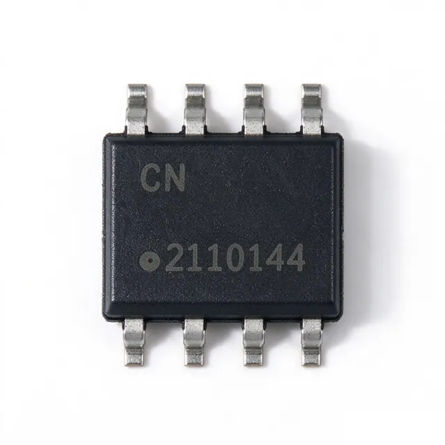
The Microchip Technology ATECC608B-SSHDA-T is a member of the CryptoAuthentication™ family of high-security cryptographic devices that combine world-class hardware-based key storage with hardware cryptographic accelerators. It is offered in an 8-pin SOIC package with I²C interface, supports ECC-P256 (ECDH and ECDSA), SHA-256, AES-128-GCM, and provides a hardware random number generator (NIST SP 800-22 compliant) plus a monotonic counter. The device integrates 10Kb secure EEPROM for keys, certificates, and data, with built-in tamper resistance including voltage glitch and temperature tamper detection. What is a CryptoAuthentication IC? A CryptoAuthentication IC is a specialized secure element that offloads cryptographic operations from the main microcontroller and protects private keys in hardware-isolated storage. These devices sit at the foundation of the security hierarchy: CryptoAuthentication IC → secure element → hardware root-of-trust → embedded security subsystem. Unlike software-based cryptography, hardware secure elements ensure private keys never leave the silicon, dramatically reducing attack surface for IoT devices, network accessories, and edge nodes where MCU resources are limited but trust is non-negotiable. The ATECC608B features a full ECDH/ECDSA engine operating in approximately 13 ms for sign operations and SHA-256/HMAC hardware acceleration, dramatically reducing cryptographic workload on host MCUs. It supports standard I²C up to 1 Mbps with configurable I²C addresses, an optional single-wire interface (SWI) variant, and operates from 2.0V to 5.5V supply with deep-sleep current as low as <150 nA. Internal EEPROM is locked through one-way fuses, preventing post-deployment firmware or key extraction by physical or remote attacks. Typical applications include Matter/Thread device authentication, secure boot for Linux/Windows IoT edge nodes, AWS IoT multi-account registration, IP protection and firmware anti-cloning, accessory and consumable authentication (medical, industrial, printer cartridges), and TLS 1.2/1.3 mutual authentication offload for resource-constrained MCUs. The device ships with Microchip's CryptoAuthLib, which provides a unified API across the entire CryptoAuthentication family. When designing with the ATECC608B, ensure I²C pull-ups are present (the SOIC version uses standard I²C, not SWI), allocate a dedicated 7-bit I²C address, and provision keys via the Microchip CryptoEvaluation kit during development. The GPIO pin can be used as a power-on reset indicator or wake source. Migration from ATECC608A is software-compatible via CryptoAuthLib. This page synthesizes distributor pricing, drop-in same-package alternatives, and practical design notes not consolidated in the manufacturer datasheet alone.

ATM90E36A-AU - 3-Phase Energy Metering AFE, 48-TQFP | Microchip
The Microchip (formerly Atmel) ATM90E36A-AU is a high-performance, poly-phase energy metering analog front-end (AFE) IC designed for three-phase four-wire (3P4W, Y0) and three-phase three-wire (3P3W, Y or Δ) systems, supplied in a 48-pin TQFP (7x7 mm) package. It integrates seven input channels (three voltage, four current) and provides active, reactive, and apparent energy computation with 0.1% accuracy over a wide dynamic range of 1000:1. The device operates from a 3.3V analog/digital supply with 1.8V internal logic support. An energy metering AFE (analog front-end) is a mixed-signal IC that combines sigma-delta ADCs, anti-aliasing filters, a DSP-based measurement engine, and digital calibration blocks. AFEs sit between current transformers / shunt resistors / voltage dividers and a host microcontroller, converting the analog line signals into computed energy quantities, RMS values, THD, and phase angles. Within the broader hierarchy, an energy metering AFE belongs to power management ICs and is typically classified as a data acquisition / signal chain IC in industrial metering subsystems. Key features include a built-in digital signal processor (DSP) for on-chip computation of mean active/reactive/apparent power, RMS voltage and current, power factor, line frequency, and harmonic distortion (THD) up to the 21st order. The IC exposes three configurable CF (calibration frequency) pulse outputs for active/reactive/apparent energy, plus three zero-crossing detection pins (ZX0/ZX1/ZX2) and three interrupt/warning outputs (IRQ0, IRQ1, WarnOut). Communication to the host MCU is via an SPI/UART selectable serial interface at up to 4 Mbps. Architecturally, the ATM90E36A-AU uses simultaneous sampling 16-bit second-order sigma-delta ADCs per channel with integrated digital integrators, eliminating the need for an external analog anti-aliasing filter on each current channel. On-chip temperature compensation and per-phase gain/phase calibration registers allow meter class 0.5S / 1.0 accuracy. The -AU suffix indicates the industrial temperature grade (-40C to +85C). Typical applications include three-phase smart electricity meters, sub-metering in solar PV and energy storage inverters, EV charging station billing, data acquisition terminals, power quality monitors, and industrial three-phase motor energy dashboards. The wide 1000:1 dynamic range also supports both CT-based and Rogowski-coil current sensors. The TQFP-48 footprint suits both through-hole-friendly reflow designs and retrofit metering modules. When designing with this part, pay attention to the SPI/UART mode selection pin and ensure the host MCU firmware matches the configured baud rate or clock polarity; mismatch is the most common bring-up issue. Decouple AVDD/DVDD with low-ESR 10uF plus 100nF ceramic pairs and provide a clean analog ground island to achieve the rated accuracy at low currents. This page synthesizes distributor pricing, drop-in package alternatives, and practical calibration notes not found in the bare manufacturer datasheet, with cross-references verified against the M90E36A datasheet revision and Microchip product family page.

ATMXT112S-MAUR - 112-Node maXTouch Touch Controller | Microchip
The Microchip Technology ATMXT112S-MAUR is a maXTouch S-Series capacitive touchscreen controller IC with 112 mutual-capacitance sensing nodes, housed in a 32-pin UQFN (4x4 mm) package. It supports screens up to 3.5 inches and delivers smartphone-grade multi-touch performance with integrated noise mitigation for operation in noisy environments. A capacitive touch controller is a mixed-signal IC that measures tiny capacitance changes on a touch sensor grid, converts them into touch coordinates, and communicates them to a host processor. In the system hierarchy, a touchscreen controller sits between the touch sensor (ITO pattern on glass or film) and the host MCU or application processor, forming part of the human-machine interface subsystem alongside display drivers and haptic feedback devices. Key features of the ATMXT112S-MAUR include its 112-node sensing matrix for dense electrode layouts, the maXTouch S-Series architecture optimized for small displays up to 3.5 inches, and an advanced noise mitigation system that rejects interference from display drivers and chargers. The device integrates acquisition logic and post-processing, offloading touch detection from the host CPU. Technically, the maXTouch S-Series uses a proprietary acquisition engine with mutual-capacitance scanning and built-in self-calibration. Configuration data is stored on-chip in nonvolatile memory, and communication with the host uses an I2C-compatible interface. The device supports moisture and gloved-finger handling modes and provides robust reporting rates for responsive user interfaces. Typical applications include feature phone touchscreens, handheld game consoles, digital still cameras, portable GPS navigation devices, and small industrial HMI panels. Any battery-powered product with a 3.5-inch or smaller capacitive display benefits from the low-power touch wake-up and high noise immunity. Design consideration: because touch performance depends strongly on the sensor pattern and panel stack-up, use Microchip's maXTouch configuration tooling and reference sensor designs; improper grounding near display VCOM lines is the most common source of false touches. This page synthesizes distributor pricing, drop-in alternatives, and practical design notes not found in the manufacturer datasheet.

ATMXT1386-Z2UIR - maXTouch 1386-Node Touch Controller | Microchip
The Microchip Technology ATMXT1386-Z2UIR is a capacitive touch screen controller from the maXTouch product platform, implementing a 1386-node multi-chip solution (4 chips) that combines charge-transfer acquisition technology with a powerful 32-bit AVR microcontroller core. It is supplied in a 64-terminal HVQCCN (LCC64) surface-mount package. A capacitive touch controller is an interface IC that measures changes in capacitance across a touch sensor grid, converts those measurements into touch coordinates, and communicates them to a host processor. Within the semiconductor hierarchy it sits under data acquisition ICs, specifically touch screen converters and controllers, and forms part of the broader human-machine interface (HMI) signal chain that includes the sensor glass, the controller IC, and the host firmware. Key differentiating features include the 1386-node acquisition capacity, which supports large-format touch panels with many simultaneous sensing channels; the multi-chip architecture that lets four devices cooperate on a single panel; and the integrated 32-bit AVR processing that performs filtering and gesture detection on-chip, reducing host CPU load. The maXTouch platform firmware can be updated in-system, enabling tuning for different glass stack-ups. The charge-transfer acquisition technique offers strong signal-to-noise performance against display noise, which is important for designs where the touch sensor is integrated into or placed close to an LCD. On-chip AVR computation allows advanced touch features such as multi-touch tracking, palm rejection, and moisture compensation depending on the configured firmware. Typical applications include industrial HMI touch panels, large-format touch screens for appliances and kiosks, medical equipment control surfaces, and embedded systems requiring robust multi-touch input on medium-to-large sensor arrays. A key design consideration is that this device has been discontinued by Microchip; the manufacturer officially recommends the ATMXT1066T2 touch controller as the alternative for new designs, so availability should be confirmed before committing to a BOM. This page synthesizes distributor listings, manufacturer product-page data, and cross-reference findings, including drop-in-replacement guidance and procurement notes not found in the manufacturer datasheet.
ATMXT1386E-Z2U - maXTouch 1386-Node Touch Controller | Microchip
The Microchip Technology ATMXT1386E-Z2U is a capacitive touchscreen controller from the maXTouch product platform, implementing a 1386-node multi-chip solution built from four chips. It combines Atmel's patented QMatrix charge-transfer capacitive sensing method with a powerful 32-bit AVR microcontroller, and supports up to 16 simultaneous touches with fast response time. A capacitive touchscreen controller is a type of sensor interface IC that measures mutual capacitance changes across a touch sensor grid, classifies and tracks finger touches, and reports coordinates to a host processor. Within the system hierarchy, it sits in the signal chain between the touch sensor (a patterned ITO or similar electrode layer on the display) and the host MCU or application processor, forming part of the broader human-machine interface (HMI) subsystem. Key features include the 1386 mutual-capacitance node count, which suits medium-to-large touch panels; the patented charge-transfer acquisition engine, which delivers high signal-to-noise measurement accuracy; and multi-touch tracking of up to 16 touches. The high-performance architecture enables fast response and unlimited-touch reporting up to the 16-touch limit, making the device suitable for demanding interactive displays. Technically, the mXT1386E uses a unique charge-transfer acquisition engine implementing the QMatrix capacitive sensing method patented by Atmel. Coupled with a state-of-the-art 32-bit AVR CPU, the entire touchscreen sensing solution can measure, classify and track finger touches with a high degree of accuracy. As a multi-chip (4-chip) solution, the family coordinates sensing across the node array within one firmware-managed platform. Typical applications include tablet and e-reader touchscreens, industrial HMI panels, and consumer electronics displays requiring robust multi-touch performance with gloved-hand and noise immunity characteristic of the maXTouch platform. Design consideration: this part is a multi-chip solution, so verify board space, mechanical stacking and firmware/configuration compatibility against the replacement controller before redesign. Note that Microchip has officially recommended the ATMXT1066T2 as the alternative touch controller for this family. This page synthesizes distributor sourcing data, the manufacturer-recommended replacement, and practical design notes not found in the manufacturer datasheet.
ATMXT1386E-Z2UR - maXTouch 1386-Node Touch Controller | Microchip
The Microchip Technology ATMXT1386E-Z2UR is a 1386-node capacitive touch screen controller from the maXTouch product platform, implemented as a multi-chip solution combining four chips that pair charge-transfer acquisition technology with a powerful 32-bit AVR microcontroller core. It supports up to 16 simultaneous touches with fast response, and communicates with the host processor through either an I2C-compatible interface or a USB interface, though only one interface should be used in any single design. A capacitive touch controller is an interface IC that measures changes in capacitance across a touch sensor grid, applies touch-detection and noise-immunity algorithms, and reports touch coordinates to a host MCU or application processor. Within the semiconductor hierarchy it sits under touch screen controllers, a subcategory of sensor interface ICs in the maXTouch family spanning small single-chip solutions up to large multi-chip nodes for large-format touch panels. Key differentiating features include the very high 1386-node sensor channel count, support for up to 16 concurrent touch points, self- and mutual-capacitance charge-transfer acquisition, and dual host communication options (I2C-compatible or USB). The multi-chip architecture scales acquisition bandwidth for large touch panels used in industrial HMI and commercial display designs. Technically, the ATMXT1386E integrates four chips operating as one synchronized controller, with the 32-bit AVR execution core running Microchip's maXTouch firmware for touch detection, palm rejection, and noise filtering. Configuration is typically loaded into EEPROM/flash by the host at power-up, allowing tuning of sensitivity and gesture behavior without firmware changes. Typical applications include large-format industrial touch monitors, commercial kiosks and point-of-information terminals, and multi-touch human-machine interfaces where many sensor nodes and reliable multi-touch detection are required. A key design consideration is that Microchip has flagged this product for end-of-life: the manufacturer-recommended alternative touch controller is the ATMXT1066T2, so new designs should target that device while the ATMXT1386E family remains available for last-time-buy and service inventory. This page synthesizes distributor sourcing, the manufacturer-recommended successor, and practical design guidance not found in the standard datasheet listing.
ATMXT1386XES-CHPSET2 - 1386-Node maXTouch Touch IC | Microchip
The Microchip Technology ATMXT1386XES-CHPSET2 is a 1386-node capacitive touch screen sensor IC solution from the maXTouch product platform, supplied as a multi-chip set of 4 chips. By combining charge-transfer touch sensing technology with a powerful 32-bit AVR microcontroller core, this device delivers large-format projected-capacitive touch detection with Microchip's maXTouch signal-processing algorithms. A capacitive touch controller is a specialized mixed-signal IC that scans a matrix of mutual-capacitance nodes on a touch sensor panel, converts capacitance changes into digital coordinates, and reports touch positions to a host processor over a digital interface. In the product taxonomy, this device belongs to Interface ICs > capacitive touch sensors, which sits within the broader families of human-interface devices, sensor interfaces, and mixed-signal integrated circuits. Key characteristics of the ATMXT1386 family include the 1386-node sensing capacity, an on-chip 32-bit AVR processing core for autonomous touch acquisition, and maXTouch filtering that supports gloved operation, passive stylus, and water-rejection behavior typical of the platform. The XES-CHPSET2 ordering code denotes a chip-set (multi-chip) configuration rather than a single monolithic die, which system designers must account for in PCB partitioning. Technically, the charge-transfer acquisition engine periodically drives and senses the electrode matrix, while the embedded AVR firmware applies noise filtering, baseline tracking, and touch classification. This architecture offloads all touch processing from the host, requiring only configuration data and touch reports over the communication interface. Typical applications include large-format touchscreen displays for industrial human-machine interfaces (HMI), point-of-information kiosks, and other commercial touch systems that previously used this high-node-count controller. A key design consideration: Microchip lists the ATMXT1066T2 as the recommended alternative touch controller for the ATMXT1386, since this multi-chip solution is obsolete and no longer recommended for new designs. This page synthesizes distributor availability data, the manufacturer's recommended migration path, and drop-in alternative analysis not found on the Microchip product page alone.
ATMXT1664S1-CU - maXTouch Touchscreen Controller IC | Microchip Technology
The Microchip Technology ATMXT1664S1-CU is a maXTouch capacitive touchscreen controller IC from the maXTouch S-series family, supporting 1664 mutual-capacitance sensing nodes for projected-capacitive touch screens, supplied in a compact surface-mount package with RoHS3-compliant construction. According to distributor listings including DigiKey and Octopart, the device is classified as a Touch Screen Controller (IC SENSOR MAXTOUCH). A capacitive touchscreen controller measures mutual capacitance across a matrix of transmit and receive electrodes on the touch sensor. When a finger or passive stylus approaches the intersection of electrodes, local capacitance changes; the controller scans the matrix, converts the capacitance deltas to touch coordinates, applies gesture and noise filtering, and reports touch data to a host processor over an interface such as I2C or SPI. Touchscreen controllers sit within the broader hierarchy of sensor interface ICs and human-machine interface (HMI) semiconductors. The maXTouch S-series architecture integrates a high-performance acquisition engine with differential charge amplifiers, a configurable scan sequencer, and an embedded MCU core executing Microchip-supplied object-based firmware. Self- and mutual-capacitance fusion enables gloved-hand operation and water rejection, while frequency-hopping acquisition combats charger and display noise - a critical requirement for thin bezel tablets, POS terminals, and automotive HMI panels. Technical strengths of the family include high node counts supporting large-format touch panels, the maXTouch object model allowing configuration of key timings and thresholds via I2C registers, and mature firmware tooling through Microchip's maXTouch studio ecosystem. The S1 model designation reflects the firmware/feature configuration of the 1664-node silicon. Typical applications include 7-inch to 13-inch capacitive touchscreens in tablets, human-machine interfaces for white goods and appliances, point-of-sale and ticketing terminals, smart-home wall panels, and industrial operator panels where multi-touch and robust noise immunity are required. When designing with this controller, allocate a clean low-noise analog supply for the sensing core and route the sensor flex connector away from switching regulators; charger-mode noise often dominates real-world touch performance and must be verified with the intended display and charger pair. This page synthesizes distributor sourcing data, drop-in family alternatives, and practical design notes not found in the manufacturer datasheet, with pricing as of 2026-09-19.
ATMXT1664S1-CUR - maXTouch 1664-Channel Touch Controller | Microchip
The Microchip Technology ATMXT1664S1-CUR is a maXTouch S Series capacitive touchscreen controller with 1664 mutual-sense channels, built on a 32-bit AVR microcontroller architecture, supplied in a reflow-capable surface-mount package for large-format touchscreen devices. A capacitive touch screen controller is an interface IC that measures capacitance changes across a grid of sensor electrodes to detect finger and stylus positions. Within the system hierarchy, it sits between the raw touch sensor (ITO pattern on glass or film) and the host application processor, converting analog charge-transfer measurements into touch coordinates over a digital interface. The maXTouch family from Microchip (originally Atmel) is a widely adopted line of such controllers used from wearables to large interactive displays. The ATMXT1664S1 belongs to the S Series, which brings the maXTouch architecture to large touchscreen devices. Its 1664 sensing channels support high electrode counts typical of large-format panels, while the integrated 32-bit AVR core performs on-chip acquisition, filtering, and gesture processing, offloading the host processor. Multiple S Series devices can operate simultaneously to drive very large screens, a scalability feature documented by Microchip for this family. The suffix structure of the part number encodes ordering options such as temperature grade and packaging (-CUR indicates a reflow-eligible, RoHS-grade ordering variant per Microchip nomenclature). As with all maXTouch parts, configuration of sensitivity, report rate, and multi-touch behavior is performed via firmware objects downloaded to the controller, allowing one PCB design to be tuned for different sensor stacks. Typical applications include large interactive displays, industrial HMI panels, point-of-information kiosks, and premium consumer touch devices where high channel count and robust noise immunity near displays or chargers are required. A key design consideration is that maXTouch controllers require a configuration file matched to the specific sensor pattern and stack-up; mismatched configurations degrade linearity and report rate. Verify communication with the host over the I2C-compatible interface during bring-up. This page synthesizes distributor availability, Microchip product data, and the manufacturer-recommended replacement ATMXT1664T3 into one reference, adding drop-in alternative guidance and design notes not found in the datasheet alone.
ATMXT2952T2-C2U - maXTouch Touch Controller | Microchip
The Microchip Technology ATMXT2952T2-C2U is a maXTouch capacitive touchscreen controller IC from the mXT2952T2 family, supporting up to 2952 touch channels and display sizes up to 21 inches, aimed primarily at industrial designs and housed in a BGA package. A capacitive touchscreen controller is a mixed-signal IC that measures mutual-capacitance changes across a touch sensor grid, converts the raw charge-transfer measurements into touch coordinates and gesture information, and reports them to a host processor over a digital interface. In the system hierarchy, it sits within the human-interface / data acquisition domain: touchscreen controller -> capacitive touch sensor IC -> sensor interface IC -> mixed-signal semiconductor. Key features of the ATMXT2952T2 family include Microchip's Adaptive Sensing technology, which automatically and intelligently switches between touch operating modes based on the detected object or environment, dynamic touch classification for finger, glove, stylus, and water rejection scenarios, and a debug port for tuning (per Microchip application note QTAN0050 'Using the maXTouch Debug Port'). The device supports I2C host communication; in I2C mode the pull-up resistor on the DBG_SS/GPIO0 shared ball is optional and present only if the ball is used as DBG_SS. The architecture pairs a charge-transfer analog front end with on-chip processing that performs self- and mutual-capacitance scanning, noise filtering, and touch classification. Adaptive Sensing allows the same controller to deliver reliable touch performance on thick cover lenses, in wet conditions, and under EMI conditions typical of industrial panels. Typical applications include industrial HMI touch panels up to 21 inches, factory automation displays, medical equipment screens, and commercial kiosk or point-of-information terminals where gloved-hand and water rejection are required. A key design consideration is the shared DBG_SS/GPIO0 ball: only one of these two functions can be selected, and the circuit must be designed accordingly; consult the manufacturer datasheet and QTAN0050 before finalizing the sensor flex pin mapping. Note that Microchip identifies ATMXT2952TD as the recommended alternative touch controller for the ATMXT2952T2, which is relevant for new designs and long-term supply planning. This page synthesizes distributor availability, the recommended replacement, and design guidance not consolidated in the manufacturer datasheet.
ATMXT768E-ABR - maXTouch Touchscreen Controller | Microchip
The Microchip Technology ATMXT768E-ABR is a maXTouch mXT768E-AT mutual-capacitance touchscreen controller IC designed for projected-capacitive touchscreens of up to 10.1-inch diagonal or even larger. It belongs to Microchip's maXTouch family of capacitive touch controllers and integrates signal-acquisition, touch-decision, and host-interface functions in a single device. A projected-capacitive (PCAP) touchscreen controller is a specialized mixed-signal IC that drives excitation signals across rows and columns of a transparent ITO sensor grid and measures mutual capacitance changes at each intersection. Within the system hierarchy, it sits between the raw touch sensor laminate and the host processor, delivering pre-processed touch coordinates over a digital interface. This class of device is fundamental to modern human-machine interface (HMI) design in industrial, medical, and consumer equipment. Key characteristics of the mXT768E-AT include high responsiveness for large-format screens, support for multi-touch reporting, and Microchip's maXTouch object-based reporting architecture in which touch data is conveyed as structured objects over an I2C or SPI-compatible host interface. The device is firmware-configurable, allowing tuning of sensitivity, rejection thresholds, and gesture behavior to match specific sensor stacks. The ATMXT768E-ABR was originally targeted at tablets, industrial HMI panels, point-of-sale terminals, and medical monitors in the 7-inch to 10.1-inch class. Note that Microchip's product page indicates this part is no longer recommended for new designs and recommends the ATMXT1189TD-A as the alternative touch controller for new development. Design consideration: because the mXT768E-AT is in end-of-life transition, new designs should evaluate the ATMXT1189TD-A and verify firmware migration effort, sensor-stack compatibility, and pin mapping before committing to a layout. This page synthesizes distributor availability, cross-reference data, lifecycle status, and practical design notes not found in the manufacturer datasheet alone, helping engineers make a supply-risk-aware selection decision.
ATMXTS100-CU - maXStylus Active Stylus ASIC | Microchip
The Microchip Technology ATMXTS100-CU is a maXStylus Gen I active stylus ASIC designed for capacitive touch sensing systems, classified under Interface - Sensor, Capacitive Touch ICs and belonging to the maXTouch product series from Microchip Technology. The device ships in tape-and-reel packaging with a standard package quantity of 6,000 units per reel, and the part status is listed as Active per distributor and manufacturer data. An active stylus controller IC is a specialized mixed-signal device that implements the transmit and signal-processing functions of an active pen system, enabling a battery-powered stylus to communicate position, pressure, and hover information with a capacitive touchscreen that is driven by a companion maXTouch touch controller. Within the system hierarchy, this device sits alongside touch sensors and touch screen controllers inside the human-interface input subsystem of tablets, e-readers, signature pads, and other pen-enabled displays. Key characteristics identified from verified distributor data include the maXStylus Gen I generation designation, maXTouch series membership, capacitive touch interface classification, and active lifecycle status. This positions the ATMXTS100-CU within Microchip's established maXTouch ecosystem, which is widely deployed in commercial and industrial touchscreen designs. Architecturally, active stylus ASICs coordinate the stylus-tip signal generation and timing with the host touchscreen controller so that palm rejection, hover detection, and fine-line pen input can be achieved on standard mutual-capacitance panels. Designers typically pair the stylus ASIC with a maXTouch touchscreen controller on the host side to form a complete pen-and-touch subsystem. Typical applications include active pen input for tablets and 2-in-1 computing devices, digital signature capture terminals, and industrial touch panels requiring stylus precision. In each case the ASIC provides the dedicated stylus-side signal chain that a general-purpose MCU would struggle to replicate with equivalent latency and power efficiency. A key design consideration is that per available cross-reference information this device is generally not pin-compatible with capacitive touch sensors from competing vendors, so second-sourcing requires careful I/O voltage and interface evaluation. This page synthesizes distributor pricing channels, verified lifecycle data, and practical design notes not consolidated in the manufacturer datasheet.

ATPL230A-AKU-R - PRIME PLC Modem 128.6Kbps | Microchip
The Microchip Technology ATPL230A-AKU-R is a PRIME-compliant power line communications (PLC) base band modem IC delivering data rates up to 128.6 kbps from a 3.3 V supply in an 80-pin LQFP (12x12 mm) package. It integrates an AES-128 crypto engine, operates from -40C to +85C, and supports CENELEC-A, FCC, and ARIB frequency bands. A power line communications modem is a specialized embedded device that transmits data over existing AC mains or DC power distribution wiring, eliminating the need for dedicated communication cabling. In the system hierarchy, the ATPL230A belongs to the class of application-specific microcontrollers and communication transceivers, bridging the gap between a host MCU and the physical power-line medium via an analog front end and coupling network. Key features include full compliance with the PHY layer of the PRIME (PRoducts for Intelligent Metering Evolution) specification v1.3 and v1.4, independently selectable transmission bands up to 472 kHz, and baud rates ranging from 5.4 kbps to 128.6 kbps. Additional robust modes and frequency band extension improve link reliability in noisy grid environments, while the hardware AES-128 engine secures metering data without burdening the host processor. The ATPL230A uses a flexible architecture composed of hardware accelerators and co-processors, enabling a highly efficient PRIME PHY implementation. An SPI interface connects the modem to an external host microcontroller, which handles PRIME MAC/CON layers and application logic. This partitioning allows firmware upgrades on the host without touching the certified PHY layer. Typical applications include smart metering (electricity, gas, water), smart grid street lighting control, solar inverter communication, and building automation over mains wiring. The industrial temperature grade of -40C to +85C supports outdoor and cabinet-mounted metering equipment. When designing with this device, budget the analog front end (line driver, coupling transformer, and filters) carefully, as PHY performance in CENELEC-A, FCC, and ARIB bands depends strongly on the external network; Microchip reference designs should be followed for coupling circuitry. This page synthesizes distributor pricing, drop-in alternatives, and practical design notes not found in the manufacturer datasheet.
ATPL250A-AKU-R - G3-PLC Power Line Modem IC | Microchip
The Microchip Technology ATPL250A-AKU-R is a G3-PLC (Power Line Communication) modem system-on-chip delivered in an 80-pin LQFP (AKU) surface-mount package, rated for the industrial temperature range of -40C to +85C and supplied in Tape & Reel (T&R) green/RoHS packaging. It integrates hardware accelerators and coprocessors that achieve a highly efficient G3 PHY layer implementation for narrowband power line communication. A power line communication modem is a communication IC that transmits data over existing AC mains or DC power lines by modulating a carrier signal onto the line, eliminating the need for dedicated wiring. Within the system hierarchy, the ATPL250A sits between the physical analog line front end and the host microcontroller, offloading the computationally demanding PHY and MAC layers of the G3-PLC standard from the application processor. G3-PLC is an open standard promoted by the G3-PLC Alliance and supported by internationally recognized standards bodies, making it the dominant PLC technology for smart grid infrastructure. Key features include flexible support for G3-PLC CENELEC, ARIB, and FCC frequency profiles, which allows one design to serve global markets with different regulatory band plans. The hardware-accelerated architecture handles OFDM modulation, forward error correction, and convolutional interleaving in dedicated logic, delivering deterministic real-time performance that a pure software implementation cannot match. The device is classified by distributors as a Network Controller & Processor IC / power line communications microcontroller. The ATPL250A implements the G3 PHY layer with hardware accelerators and coprocessors, achieving spectral efficiency and robustness over hostile power line channels characterized by multipath fading, impulsive noise, and frequency-selective attenuation. This architecture lets a companion host MCU manage application logic, metering computation, or protocol translation while the ATPL250A transparently maintains the PLC link, including adaptive tone mapping and channel estimation. Typical applications include smart metering (electricity meters and data concentrators), smart lighting control, industrial and home automation, and home energy management gateways. In a data concentrator, the ATPL250A aggregates PLC traffic from hundreds of meters onto a backhaul link, making its PHY efficiency directly responsible for network capacity. When designing with the ATPL250A, pay close attention to the analog line driver and coupling network: PCB layout of the transmit path and use of the reference design from the Atmel/Microchip user manual are critical to meeting G3-PLC Alliance interoperability and local emissions regulations. This page synthesizes verified distributor data, drop-in alternatives from the same LQFP-80 ATPL PLC family, and selection guidance not consolidated in the manufacturer datasheet. Pricing and availability were last verified on 2026-09-19.
ATPL250A-AKU-Y - G3-PLC Power Line Modem 3.3V | Microchip
The Microchip Technology ATPL250A-AKU-Y is a G3-PLC (Power Line Communication) modem microcontroller IC operating from a 3.3V supply, housed in an 80-pin LQFP (AKU) package, rated for the industrial temperature range of -40C to +85C. A power line communication modem is a specialized communication IC that transmits and receives data over existing AC mains or DC power lines, eliminating the need for dedicated wiring. It sits within the broader hierarchy of communication ICs and embedded processors: PLC modem -> telecom interface IC -> network controller -> microcontroller-class system-on-chip. G3-PLC is an open standard promoted by the G3-PLC Alliance and supported by internationally recognized standards bodies, widely deployed in smart grid infrastructure. The ATPL250A features a flexible architecture composed of hardware accelerators and coprocessors that achieve a very efficient G3 PHY layer implementation. According to the Microchip ATPL250A datasheet, the device supports G3-PLC CENELEC, ARIB, and FCC profiles, making it adaptable to regional regulatory band plans across Europe, Japan, and North America. The hardware-based PHY offloads modulation, coding, and windowing tasks from software, reducing CPU load and improving real-time determinism. This combination of flexible coprocessor architecture and multi-profile band support makes the ATPL250A a compact and highly efficient device for a wide range of smart grid applications, including smart metering (smart meters and data concentrators), street lighting control, industrial and home automation, and home area network gateways. The 80-pin LQFP provides sufficient GPIO and peripheral interfaces to host application firmware alongside the modem function. When designing with the ATPL250A, careful attention must be paid to the analog front-end coupling network between the modem and the power line, as line impedance variation directly affects achievable data rate and link reliability. Microchip provides the ATPL250A Evaluation Kit (documented in device document 00002299B) as a hardware platform for evaluating the modem and integrating it into custom designs. This page synthesizes distributor pricing, drop-in family alternatives, and practical design guidance not found in the manufacturer datasheet, consolidating data from DigiKey, Mouser, Octopart, and Microchip documentation as of 2026-09-19.
AX58100LT - 2/3-Port EtherCAT Slave Controller | ASIX
The ASIX Electronics AX58100LT is a 2/3-port EtherCAT Slave Controller (ESC) with two integrated Fast Ethernet PHYs, operating from a 3.3V supply and packaged in an 80-pin LQFP-EP (10x10 mm). It implements the EtherCAT slave protocol in hardware and exposes 2 or 3 PHY ports plus digital host interfaces (SPI / host bus) to an external MCU, making it one of the most integrated single-chip ESCs in its class. An EtherCAT Slave Controller is a specialized industrial Ethernet IC that handles the EtherCAT protocol (a deterministic real-time Ethernet standard originally developed by Beckhoff and standardized by the EtherCAT Technology Group) without burdening the host CPU. The EtherCAT protocol itself falls under the broader hierarchy of industrial fieldbuses -> real-time Ethernet -> industrial communication IC -> semiconductor. The "slave" role means the device sits on the bus as a node that processes the EtherCAT datagram on the fly as it traverses each port, in contrast to an EtherCAT master which orchestrates the network. The AX58100LT integrates two 100BASE-TX Fast Ethernet PHYs directly on-die, eliminating the need for external PHY chips and reducing BOM cost, PCB area, and signal-integrity complexity for servo drives, distributed I/O, and sensor modules. With 100 Mbit/s full-duplex ports, it supports standard EtherCAT cycle times down to the 12.5 us micro-period range and the typical 1 ms motion-bus update rate. The industrial-grade -40C to +105C operating range suits it for servo, motion control, and factory automation deployments. Typical applications include EtherCAT servo motor drives, decentralized digital I/O modules, EtherCAT sensor interfaces, robotic joint controllers, EtherCAT junction or branch modules, and other industrial-automation nodes. The STM32F303RE host reference design published by ST validates AX58100LT for FOC (field-oriented control) servo loops and points designers toward proven firmware stacks. When designing with the AX58100LT, ensure the 80-pin LQFP-EP exposed pad is soldered with sufficient thermal via arrays to dissipate internal PHY power, and route the differential MDI pairs as 100-ohm differential controlled-impedance traces. The host MCU should run an ASIX-supported EtherCAT slave stack (e.g., SOES or SSC ported to the chosen MCU) to maximize bus conformance. This page synthesizes distributor pricing, LQFP-80 drop-in alternatives, and practical industrial-board design notes not found in the raw manufacturer datasheet, giving the BOM engineer a complete procurement and design entry point for EtherCAT nodes built around the AX58100LT.
B50280C1KFBG - Octal 10/100/1000 PHY Transceiver | Broadcom
The Broadcom B50280C1KFBG is an octal 10/100/1000 Mbps Ethernet PHY transceiver integrated circuit designed for high-density networking line cards and switch aggregation. The device integrates eight independent Gigabit Ethernet physical layer transceivers in a single package, supporting full-duplex operation over twisted-pair copper media, and is targeted at enterprise switching platforms where port density and per-port power are both critical design constraints. An Ethernet PHY (Physical Layer Device) is the lowest-speed layer of the OSI networking stack, handling the analog signaling, encoding/decoding, clock recovery, and link training required to push bits over a Cat5e/Cat6 cable. PHY transceivers sit beneath the MAC and switch fabric; an octal PHY like the B50280C1KFBG aggregates eight Gigabit PHYs into one IC to simplify PCB routing, reduce component count, and minimize board area compared to using eight discrete single-port PHYs. PHY -> Ethernet transceiver -> Networking IC -> Interface IC -> Integrated Circuit is the broader hypernym chain. The B50280C1KFBG supports auto-negotiation, auto-MDI/MDIX crossover, Energy Efficient Ethernet (EEE, IEEE 802.3az), and 802.1AE MACsec readiness depending on firmware build. Each port independently negotiates 10/100/1000BASE-T, recovers clock and data, and presents GMII/RGMII to the host MAC. The integrated DSP-based echo canceller and baseline wander correction enable robust 100m Cat5e link performance without external magnetics beyond the standard 1:1 transformer. Typical applications include top-of-rack and leaf switches, network interface cards with multi-port PHYs, router line cards, industrial Ethernet switches, and telecom access equipment. Per-port power below ~1W and the octal integration make it especially suited for chassis switches where hundreds of Gigabit ports must be supported within thermal and power budgets. Designers should pay attention to the SGMII/SerDes reference clock architecture, the quad-port group power sequencing, and the requirement for dedicated 1:1 isolation transformers per port. PCB layout for the B50280C1KFBG demands careful 100-ohm differential pair routing for each of the eight MDI channels with strict length matching. This page synthesizes distributor pricing, package specifications, and drop-in alternatives that are not found in the manufacturer datasheet alone, providing a single reference for engineers evaluating the B50280C1KFBG against multi-port PHY options from Broadcom and competitor families.