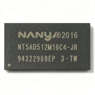
K6X0808C1D-BF55 - 256Kbit 5V Asynchronous SRAM 55ns | Samsung
MPN: K6X0808C1D-BF55 ✓ Hoạt độngK6X0808C1D-BF55 Tóm tắt
An asynchronous SRAM (Static Random Access Memory) is a type of volatile semiconductor memory that stores each bit in a bistable latch circuit made of transistors, and unlike DRAM it never requires refresh cycles. Because access is asynchronous - controlled directly by address and chip-enable timing rather than a clock - it provides deterministic, simple read and write operations. Within the memory hierarchy, SRAM sits above DRAM in speed and cost, and this parallel SRAM family occupies the classic embedded-memory slot historically used for buffering, scratchpad, and code/data storage in microprocessor-based systems.
Key features include a 5 V single supply operation, a fast 55 ns address access time, and the low stand-by and operating power typical of Samsung's advanced CMOS process technology. The K6X0808C1D family supports various operating temperature ranges and multiple package options, giving designers system-level flexibility. The three control pins (CE, OE, WE) provide standard parallel-SRAM bus interfacing with glueless connection to most 8-bit and 16-bit microcontrollers and CPUs.
Technically, the device uses Samsung CMOS SRAM process technology with a standard asynchronous timing architecture: address setup, chip-enable access, output-enable access, and write-cycle timings are all specified in the manufacturer datasheet. Data retention in stand-by is achieved with CE deselected, which keeps power consumption minimal in battery-backed or intermittently powered designs.
Typical applications include industrial control systems, networking and telecom line-card buffers, test and measurement instrumentation, legacy embedded designs requiring second-sourceable 32K x 8 memory, and battery-backed data logging where deterministic asynchronous access is preferred over clocked memory.
When designing with this device, ensure address and control setup/hold times meet the 55 ns grade datasheet limits, and tie unused address or control lines appropriately to avoid floating inputs that increase stand-by current.
This page synthesizes distributor pricing, drop-in alternatives, and practical design notes not found in the manufacturer datasheet.
Bộ thay thế dễ dàng lắp đặt cho K6X0808C1D-BF55 — cùng gói, chân-to-chân tương thích. Các bộ phận yêu cầu hàn PCB bị loại trừ.
Các biến thể trong loạt này
Các mẫu cùng loạt có thể lắp đặt dễ dàng tương thích với K6X0808C1D-BF55 (cùng hình factor và footprint) — khác nhau ở Package, Technology, Memory Type, Organization, Data Bus Width.
K6X0808C1D-BF50
✅ Drop-In📋 Tham chiếu thay thế (không có trong danh mục)
K6X0808C1D-AF55
✅ Drop-In📋 Tham chiếu thay thế (không có trong danh mục)
K6X0808C1D-GF55000
✅ Drop-InLiên hệ để biết giá
Xem tài liệu →AS6C62256
✅ Drop-In📋 Tham chiếu thay thế (không có trong danh mục)
IS62C256AL
✅ Drop-In📋 Tham chiếu thay thế (không có trong danh mục)
K6X0808C1D-BF55 Thông số kỹ thuật
| Kiểu bộ nhớ | Asynchronous SRAM |
| Kích thước bộ nhớ | 256 Kbit |
| Tổ chức | 32K x 8 |
| Access Time | 55 ns |
| Giao diện | Parallel |
| Điện áp cung cấp | 5 V |
| Technology | CMOS |
| Hộp | 28-SOP |
| Kiểu lắp đặt | Surface Mount |
| Control Signals | CE, OE, WE |
| Memory Format | SRAM |
| Clock Frequency | N/A (asynchronous) |
| Refresh | Not required (static memory) |
| Trạng thái RoHS | unknown |
Cấu hình chân K6X0808C1D-BF55
| Chân 1 | A14 — Address input bit 14 |
| Chân 2 | A12 — Address input bit 12 |
| Chân 3 | A7 — Address input bit 7 |
| Chân 4 | A6 — Address input bit 6 |
| Chân 5 | A5 — Address input bit 5 |
| Chân 6 | A4 — Address input bit 4 |
| Chân 7 | A3 — Address input bit 3 |
| Chân 8 | A2 — Address input bit 2 |
| Chân 9 | A1 — Address input bit 1 |
| Chân 10 | A0 — Address input bit 0 |
| Chân 11 | I/O0 — Data input/output bit 0 |
| Chân 12 | I/O1 — Data input/output bit 1 |
| Chân 13 | I/O2 — Data input/output bit 2 |
| Chân 14 | GND — Ground |
| Chân 15 | I/O3 — Data input/output bit 3 |
| Chân 16 | I/O4 — Data input/output bit 4 |
| Chân 17 | I/O5 — Data input/output bit 5 |
| Chân 18 | I/O6 — Data input/output bit 6 |
| Chân 19 | I/O7 — Data input/output bit 7 |
| Chân 20 | CE — Chip enable |
| Chân 21 | A10 — Address input bit 10 |
| Chân 22 | OE — Output enable |
| Chân 23 | A11 — Address input bit 11 |
| Chân 24 | A9 — Address input bit 9 |
| Chân 25 | A8 — Address input bit 8 |
| Chân 26 | A13 — Address input bit 13 |
| Chân 27 | WE — Write enable |
| Chân 28 | VCC — Power supply (+5 V) |
Ứng dụng tiêu biểu
K6X0808C1D-BF55 phù hợp cho 6 Áp dụngs: Industrial Control and PLC Systems, Telecom and Networking Line-Card Buffers, Test and Measurement Instrumentation, Legacy Embedded Design Maintenance and Second Sourcing, Battery-Backed Data Logging, Automotive Diagnostic and Test Fixtures.
Industrial Control and PLC Systems
Industrial controllers built around 5 V 8-bit MCUs (8051-class, H8, or legacy 68HC11 platforms) frequently need scratchpad and data-log memory on a 5 V parallel bus. The K6X0808C1D-BF55 fits these designs exactly: its 5 V CMOS I/O levels are native to the host bus, its 55 ns access time exceeds the 1-2 MHz effective bus rates of such controllers with large timing margin, and its CE/OE/WE control interface requires no glue logic. Mounted in a 28-SOP surface-mount package, it survives the vibration and thermal cycling typical of factory-floor equipment. Its asynchronous operation removes any clock-skew concerns in electrically noisy cabinets, and CMOS low stand-by current keeps data intact through powered-down intervals when combined with a backup cell.
Được đề xuất
Telecom and Networking Line-Card Buffers
Legacy telecom line cards and networking backplanes historically used 5 V parallel SRAM for packet staging, counters, and configuration scratchpads. The K6X0808C1D-BF55 serves this role with a 55 ns access time that comfortably meets classic 8- and 16-bit CPU bus timings (12-25 MHz class), while its 32K x 8 organization maps directly to segment-addressed buffering schemes. Because the part is asynchronous, data path latency is deterministic - valuable for TDM framers and interrupt-driven firmware that must predict memory turnaround. Samsung's CMOS process limits operating power, important in cards dissipating budget on many memory chips, and CE-deasserted stand-by reduces drain on sparsely accessed banks.
Được đề xuất
Test and Measurement Instrumentation
Bench instruments, data loggers, and ATE fixtures often retain a 5 V parallel memory bank for calibration constants, waveform capture staging, or state-machine context. The K6X0808C1D-BF55 is attractive here because access timing is fully asynchronous and predictable at 55 ns, simplifying worst-case timing analysis in mixed-speed instrument buses. The 8-bit wide I/O matches the byte-oriented DMA channels common in measurement front-ends, and the SOP package permits dense multi-bank arrays on the same footprint. Combined with a power-fail supervisor and backup source, CMOS stand-by retention preserves calibration data through outages without EEPROM write-wear concerns.
Được đề xuất
Legacy Embedded Design Maintenance and Second Sourcing
Many fielded 5 V embedded platforms - medical service tools, avionics ground equipment, point-of-sale terminals - specify a Samsung K6X SRAM by name but face supply-chain risk on legacy memory. The K6X0808C1D-BF55 remains procurable (listed 'ships today' on DigiKey and stocked across 8 distributors per Octopart), and the same-family BF50/AF55/G-grade variants plus 62256-compatible Alliance and ISSI parts give procurement a genuine second-source map on an identical 28-pin footprint. Engineering teams can therefore maintain form-fit-function continuity without PCB respin, using drop-in SOP replacements that share CE/OE/WE control conventions and 5 V CMOS levels.
Được đề xuất
Battery-Backed Data Logging
Energy meters, vending controllers, and remote sensors store accumulated data in nonvolatile-capable SRAM banks built from a 5 V SRAM plus backup cell and supervisor. The K6X0808C1D-BF55 is a strong fit: as static CMOS memory it consumes only stand-by current with CE deselected (see Samsung family datasheet for exact figures), needs no refresh cycles, and its write endurance is effectively unlimited, avoiding the wear-out limits of flash. A comparator-gated chip-enable holds data through brownouts, and the 55 ns access time ensures no timing penalty when the logger wakes to append records. The SOP surface-mount footprint suits compact logger boards.
Được đề xuất
Automotive Diagnostic and Test Fixtures
Bench fixtures and diagnostic stations servicing 5 V automotive ECUs frequently emulate or intercept ECU memory buses, requiring SRAM with native 5 V CMOS thresholds and standard parallel control. The K6X0808C1D-BF55's 55 ns access and 32K x 8 organization let a fixture CPU transparently shadow ECU address windows, while the SOP package allows fixture-grade rework and replacement. Because the device is asynchronous, emulated memory responds like the original EPROM/SRAM timing without added clocking logic, and generous access-time margin tolerates the cable inductance typical of fixture harnesses. Note: verify temperature grading against the Samsung datasheet for in-vehicle rather than bench-only use.
Được đề xuất
Tóm tắt các sản phẩm được đề xuất
Dữ liệu tham khảo kỹ thuật cho K6X0808C1D-BF55 — so sánh, hướng dẫn thiết kế và thông tin tuân thủ.
Hướng dẫn chọn lựa
So sánh với các sản phẩm thay thế
| Tham số | Sản phẩm này | K6X0808C1D-BF50 | K6X0808C1D-AF55 | AS6C62256 | IS62C256AL |
|---|---|---|---|---|---|
| Package | 28-SOP | 28-SOP - same | 28-SOP - same | SOP-28 (62256 footprint) - same | SOP-28 (62256 footprint) - same |
| Brand | Samsung Electronics | Samsung Electronics | Samsung Electronics | Alliance Memory | ISSI / Renesas Electronics |
| Organization | 32K x 8 (256 Kbit) | 32K x 8 (256 Kbit) | 32K x 8 (256 Kbit) | 32K x 8 (256 Kbit) | 32K x 8 (256 Kbit) |
| Supply Voltage | 5 V | 5 V | 5 V | 5 V | 5 V |
| Interface | Asynchronous parallel (CE/OE/WE) | Asynchronous parallel | Asynchronous parallel | Asynchronous parallel | Asynchronous parallel |
| Memory Type | CMOS SRAM (no refresh) | CMOS SRAM | CMOS SRAM | CMOS SRAM | CMOS SRAM |
| Pin Compatibility | 62256-style 28-pin | Identical family pinout | Identical family pinout | 62256-compatible | 62256-compatible |
Bảo phân biệt quan trọng
- Fastest readily available same-family grade margin (vsK6X0808C1D-BF50)
- Same-family second sourcing without respin (vsK6X0808C1D-AF55)
- Native 5 V CMOS bus levels (vsIS62C256AL)
Ghi chú thiết kế
Keep address and data traces short and matched where possible; at 55 ns access timing the part tolerates typical microcontroller bus stubs, but long ribbon-cable fixture wiring adds inductance and reflections that erode setup margins. Series-terminate data lines (22-33 ohm) if bus length exceeds roughly 15 cm, and verify read-data setup at the CPU against the datasheet access-time specification including output-enable delay.
Place a 0.1 uF ceramic decoupling capacitor directly across VCC/GND at pins 28/14 of the 28-SOP. During deselect, keep CE high to enter CMOS stand-by for minimum current in battery-backed designs - a floating CE via pull-down of a triad can leave input buffers switching and multiply stand-by drain. Tie OE high during write cycles to avoid bus contention on the I/O pins.
Do not operate this 5 V SRAM from a 3.3 V rail; VIH thresholds will not be met and the access-time spec is voided. Also confirm the SOP body width variant when second-sourcing: some 62256-compatible parts ship in both wide (330 mil) and narrow (300/207 mil) SOP bodies, which are NOT footprint-identical. Check the temperature-grade suffix against your ambient range using the Samsung family datasheet, not competitor conventions.
Thông tin tuân thủ
Compliance status not stated in the provided web data; verify against Samsung product documentation before design-in for regulated markets.