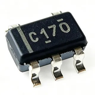
SN74LV1T125DBVR - 1-Bit Buffer/Level Shifter SOT-23-5 | TI
MPN: SN74LV1T125DBVR ✓ Hoạt độngSN74LV1T125DBVR Tóm tắt
A logic level shifter is an integrated circuit that translates signals between circuits operating at different voltage domains, such as a 3.3 V microcontroller interfacing with a 1.8 V sensor. The SN74LV1T125 belongs to TI's LV1T family of single-gate CMOS logic with reduced input thresholds, sitting within the broader hierarchy of buffer/driver -> logic gate -> standard logic IC -> semiconductor. Its wide-input tolerance eliminates the need for external pull-ups or level-shift circuits in mixed-voltage designs, simplifying PCB layout and reducing BOM cost.
Key differentiating features include 5 V tolerant inputs that enable down-translation (e.g., 3.3 V input to 2.5 V output at VCC = 2.5 V), schmitt-trigger inputs for slow or noisy edges, low Ioff (partial-power-down support) for live-insertion scenarios, and ±8 mA balanced output drive. Typical propagation delay is around 3 to 5 ns at 5 V, suitable for moderate-speed control and data paths rather than high-speed SERDES interfaces.
Architecturally, the device uses a standard CMOS buffer topology with a 3-state output stage. The OE-bar input gates the output enable line directly to the output PMOS/NMOS pair; when OE is high, both output transistors are off and the pin presents high impedance. The reduced input-threshold design lets a 1.8 V input reliably switch a 5 V VCC rail, which simplifies system design when interfacing legacy 5 V peripherals with modern low-voltage controllers.
Typical applications include GPIO expansion on low-voltage MCUs, voltage translation between 1.8 V, 2.5 V, 3.3 V, and 5 V logic domains, signal buffering on long PCB traces or cables, bus isolation between multiple processors, and reset or enable signal distribution. Designers favor it for cost- and space-constrained designs that need a true single-gate solution without paying for an unused quad buffer.
When designing with this part, ensure that the OE pin is driven to a valid logic level (never left floating) because an undriven enable can cause shoot-through or undefined output states. Decouple VCC with a 100 nF ceramic capacitor placed within a few millimeters of the supply pin, and remember that partial-power-down (Ioff) only protects the output when VCC = 0 V; inputs above VCC will still forward-bias protection diodes if VCC is present.
This page synthesizes distributor pricing, drop-in alternatives, and practical design notes not found in the manufacturer datasheet alone, helping engineers quickly evaluate the SN74LV1T125DBVR for new designs and second-source strategies.
Bộ thay thế dễ dàng lắp đặt cho SN74LV1T125DBVR — cùng gói, chân-to-chân tương thích. Các bộ phận yêu cầu hàn PCB bị loại trừ.
Các biến thể trong loạt này
Các mẫu cùng loạt có thể lắp đặt dễ dàng tương thích với SN74LV1T125DBVR (cùng hình factor và footprint) — khác nhau ở Function, Logic Family, MSL Level, Operating Temperature, Output Type.
SN74LV1T125DCKR
✅ Drop-In ⚠️ Thông số chưa được xác minh📋 Tham chiếu thay thế (không có trong danh mục)
SN74LVC1G125DBVR
✅ Drop-InLiên hệ để biết giá
Xem tài liệu →SN74LV1T126DBVR
✅ Drop-In📋 Tham chiếu thay thế (không có trong danh mục)
74LV1T125GW
✅ Drop-In📋 Tham chiếu thay thế (không có trong danh mục)
NL17SZ125DFT2G
✅ Drop-In📋 Tham chiếu thay thế (không có trong danh mục)
XC7SET125GW
✅ Drop-In📋 Tham chiếu thay thế (không có trong danh mục)
SN74LV1T125DBVR Tỷ lệ tối đa & tính chất điện
| Chức năng | Single Buffer / Non-Inverting Gate |
| Logic Family | LV1T (CMOS, reduced threshold) |
| Number of Bits per Element | 1 |
| Number of Elements | 1 |
| Kiểu đầu ra | 3-State (active-low OE) |
| VCC Range | 1.8 V to 5.5 V |
| Input Voltage Tolerance | Up to 5.5 V (independent of VCC) |
| Output Drive (IOH/IOL) | ±8 mA at VCC = 5 V |
| Ioff (Partial-Power-Down) | Supported |
| Nhiệt độ hoạt động | -40 C to +125 C |
| Hộp | SOT-23-5 (DBV) |
| Kiểu lắp đặt | Surface Mount |
| Cấp MSL | 1 (per verified data) |
| Trạng thái RoHS | Compliant |
| Lead-Free | Yes |
Cấu hình chân SN74LV1T125DBVR
| Chân 1 | OE — Output Enable, active LOW (high = high-Z output) |
| Chân 2 | A — Data input |
| Chân 3 | GND — Ground |
| Chân 4 | Y — 3-state data output |
| Chân 5 | VCC — Supply voltage (1.8 V to 5.5 V) |
Ứng dụng tiêu biểu
SN74LV1T125DBVR phù hợp cho 6 Áp dụngs: Mixed-Voltage GPIO Level Translation, Single-Line Signal Buffering on Long Traces, Reset and Enable Signal Distribution, Industrial Control and Automation, Portable and Battery-Powered Devices, Test and Measurement Equipment.
Mixed-Voltage GPIO Level Translation
The SN74LV1T125DBVR is widely used to translate signals between 1.8 V, 2.5 V, 3.3 V, and 5 V logic domains, such as connecting a 1.8 V sensor to a 3.3 V MCU. Its 5 V tolerant inputs and 1.8-5.5 V VCC range let a single part handle down-translation (3.3 V to 2.5 V at VCC = 2.5 V) without external pull-ups. The 3-state OE enables bidirectional bus sharing between two controllers, and the ±8 mA drive comfortably handles typical GPIO loads. Per TI's datasheet, this part reduces BOM count by replacing discrete resistor-divider level shifters in cost-sensitive designs.
Được đề xuất
Single-Line Signal Buffering on Long Traces
For board-to-board or cable-driven single-ended signals, the SN74LV1T125DBVR provides a clean CMOS buffer that restores logic levels on long PCB traces or backplane connections. Its ±8 mA drive handles capacitive loads that would otherwise slow down MCU GPIO edges, and the SOT-23-5 footprint fits easily near connectors. The 3-state output allows the signal to be disconnected for diagnostics or bus sharing. According to TI's design guidance, the LV1T family reduces transmission-line ringing on traces over 50 mm by providing a controlled-impedance driver.
Được đề xuất
Reset and Enable Signal Distribution
The SN74LV1T125DBVR is commonly used to fan out a single reset or enable signal to multiple ICs while isolating the source with its 3-state OE. This prevents back-driving issues when subsystems are powered down and allows orderly power-up sequencing. Its 1.8-5.5 V VCC compatibility means the same buffer IC works across mixed-voltage subsystems (e.g., 1.8 V SoC + 3.3 V peripheral). The Ioff feature ensures no leakage paths when VCC = 0, making it suitable for hot-swap or live-insertion cards.
Được đề xuất
Industrial Control and Automation
In industrial PLC and sensor-interface modules, the SN74LV1T125DBVR buffers 24 V-to-3.3 V translated logic signals between optocouplers and a low-voltage MCU. The -40 C to +125 C operating range handles factory-floor temperature extremes, while the SOT-23-5 package is robust enough for conformal-coated boards. According to TI's industrial portfolio documentation, single-gate LV1T devices are preferred in distributed I/O designs where PCB space is at a premium and channel count is low.
Được đề xuất
Portable and Battery-Powered Devices
The SN74LV1T125DBVR is well-suited for battery-powered wearables and portable instruments that must interface 1.8 V sensors with 3.3 V MCUs. Its low quiescent current and partial-power-down Ioff feature prevent leakage when the device is unpowered, extending battery life. The wide VCC range allows a single buffer to operate directly from a lithium-ion cell (2.7-4.2 V) without an additional regulator. Per TI's portable-design collateral, single-gate buffers are recommended in energy-harvesting designs where every microamp counts.
Được đề xuất
Test and Measurement Equipment
In bench instruments and data-acquisition modules, the SN74LV1T125DBVR provides level translation between legacy 5 V test circuitry and modern 3.3 V FPGAs or processors. Its fast propagation delay (typically 3-5 ns at 5 V) preserves signal integrity in measurement paths, and the 3-state output allows the FPGA to disconnect from the bus during calibration. The SOT-23-5 package integrates easily into dense probe-station PCBs. TI application notes recommend LV1T buffers for instrumentation requiring wide-input tolerance and predictable output drive.
Được đề xuất
Tóm tắt các sản phẩm được đề xuất
Dữ liệu tham khảo kỹ thuật cho SN74LV1T125DBVR — so sánh, hướng dẫn thiết kế và thông tin tuân thủ.
Hướng dẫn chọn lựa
So sánh với các sản phẩm thay thế
| Tham số | Sản phẩm này | SN74LVC1G125DBVR | SN74LV1T126DBVR | 74LV1T125GW | NL17SZ125DFT2G | XC7SET125GW |
|---|---|---|---|---|---|---|
| Brand | Texas Instruments | Texas Instruments | Texas Instruments | Nexperia | onsemi | Nexperia |
| Package | SOT-23-5 (DBV) | SOT-23-5 (DBV) - same | SOT-23-5 (DBV) - same | SOT-23-5 - same | SOT-23-5 - same | SOT-23-5 - same |
| VCC Range | 1.8 V to 5.5 V | 1.65 V to 5.5 V | 1.8 V to 5.5 V | 1.8 V to 5.5 V | 1.65 V to 5.5 V | 4.5 V to 5.5 V |
| Input Tolerance | 5.5 V tolerant | 5.5 V tolerant | 5.5 V tolerant | 5.5 V tolerant | 5.5 V tolerant | 5.5 V tolerant |
| OE Polarity | Active-Low (OE-bar) | Active-Low | Active-High (inverted) | Active-Low | Active-High | Active-Low |
| Output Drive (5 V) | ±8 mA | ±32 mA | ±8 mA | ±8 mA | ±32 mA | ±8 mA |
| Operating Temperature | -40 C to +125 C | -40 C to +125 C | -40 C to +125 C | -40 C to +125 C | -40 C to +125 C | -40 C to +85 C |
| Unit Price (qty 1) | $0.41 | $0.30 | $0.41 | $0.38 | $0.35 | $0.30 |
Bảo phân biệt quan trọng
- Reduced input threshold for true 1.8 V-to-5 V translation (vsSN74LVC1G125DBVR)
- 5 V input tolerance independent of VCC (vsSN74LV1T126DBVR)
- Cross-brand second-source availability (vs74LV1T125GW (Nexperia))
Ghi chú thiết kế
Estimated: At VCC = 3.3 V and ±8 mA continuous output drive, the SN74LV1T125DBVR draws less than 1 mA quiescent current and dissipates under 30 mW worst case. A 100 nF X7R decoupling capacitor placed within 5 mm of the VCC pin is sufficient for typical logic-edge transitions. For systems with high dI/dt on adjacent output lines, add a bulk 1-10 uF tantalum or ceramic capacitor near the supply rail to suppress ground bounce.
Never leave the OE pin floating; tie it to GND (for always-enabled) or to a controller GPIO with a defined logic level. A floating OE can cause shoot-through in the 3-state output stage, increasing quiescent current and producing undefined logic levels on Y. Also note that the Ioff feature only blocks output leakage when VCC = 0 V; if the input is driven above VCC while VCC is present, the internal ESD diodes may conduct.
Place the SOT-23-5 footprint with pin 1 dot/orientation matching TI's recommended land pattern (IPC-7351 nominal). Keep the input trace and output trace separated to minimize feedback through the package substrate. For high-speed (>10 MHz) applications, use a continuous ground plane under the IC to provide a low-impedance return path. If using the part for cable driving, add a series 33 ohm resistor near the output to dampen transmission-line ringing.
Thông tin tuân thủ
RoHS compliant per TI product page; MSL 1; not AEC-Q100 qualified (industrial/consumer use only).