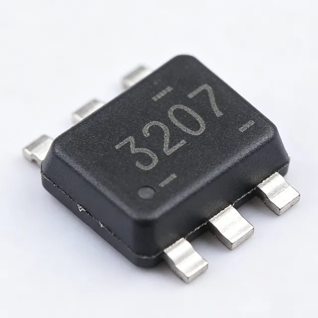
TPS563207DRLR - 3A 17V Synchronous Buck Converter | TI
MPN: TPS563207DRLR ✓ Hoạt độngTPS563207DRLR Tóm tắt
A DC-DC switching regulator (step-down converter) converts a higher input voltage to a lower regulated output using power MOSFET switches, an inductor, and output capacitors. Synchronous buck converters replace the freewheeling diode with a second MOSFET for higher efficiency. Within the power-management IC hierarchy, the TPS563207 is a monolithic buck regulator with integrated high-side and low-side FETs.
Key features include D-CAP2 mode control for fast transient response and support of low-ESR output capacitors such as specialty polymer and ultra-low-ESR ceramic types. Fixed-frequency operation in Forced CCM (FCCM) mode maintains small output ripple even at light loads. The 3-A rating with integrated FETs minimizes external component count, and the tiny SOT-563 footprint suits dense PCB layouts. The device is specified from -40C to +125C junction temperature.
Internally, D-CAP2 control combines a wide-bandwidth error amplifier with an adaptive on-time generator, enabling near-constant frequency operation and quick response to load steps with minimal output capacitance. Internal compensation and soft-start reduce design effort and board area.
Typical applications include 5 V and 12 V rail point-of-load regulation for networking equipment, SSDs and storage, industrial PCs, FPGA/ASIC auxiliary rails, and consumer electronics. The 17-V maximum input covers 12-V buses with margin.
Design tip: choose the inductor value and output capacitors per the TI datasheet equations; FCCM mode favors low ripple, while the 0.806-V feedback reference supports low-voltage cores. Verify thermal performance, as the small DRL package dissipates heat mainly through the PCB.
Bộ thay thế dễ dàng lắp đặt cho TPS563207DRLR — cùng gói, chân-to-chân tương thích. Các bộ phận yêu cầu hàn PCB bị loại trừ.
Các biến thể trong loạt này
Các mẫu cùng loạt có thể lắp đặt dễ dàng tương thích với TPS563207DRLR (cùng hình factor và footprint) — khác nhau ở Maximum Output Current, Output Voltage Range, Package, Input Voltage Range, Topology.
TPS563207SDRLR
📋 Tham chiếu thay thế (không có trong danh mục)
TPS563201DRLR
📋 Tham chiếu thay thế (không có trong danh mục)
TPS563208DRLR
📋 Tham chiếu thay thế (không có trong danh mục)
TPS563211DRLR
📋 Tham chiếu thay thế (không có trong danh mục)
TPS563212DRLR
📋 Tham chiếu thay thế (không có trong danh mục)
TPS56A207DRLR
📋 Tham chiếu thay thế (không có trong danh mục)
TPS563207DRLR Tỷ lệ tối đa & tính chất điện
| Cấu trúc | Synchronous Buck (Step-Down) |
| Phạm vi điện áp đầu vào | 4.3 V to 17 V |
| Khoảng điện áp đầu ra | 0.806 V adjustable |
| Điện áp tối đa đầu ra | 3 A |
| Control Mode | D-CAP2 mode |
| Operating Mode | Forced CCM (FCCM) |
| Số lượng đầu ra | 1 |
| Kiểu đầu ra | Positive, Adjustable |
| Junction Temperature Range | -40C to +125C |
| Hộp | SOT-563 (DRL), 6-pin, 1.6 mm x 1.6 mm |
| Kiểu lắp đặt | Surface Mount |
| FET Integration | Synchronous, integrated high-side and low-side MOSFETs |
| Supported Output Capacitors | Low-ESR ceramic and specialty polymer |
| Trạng thái RoHS | Compliant |
Cấu hình chân TPS563207DRLR
| Chân 1 | EN — Enable pin, logic high enables the converter |
| Chân 2 | GND — Ground reference |
| Chân 3 | SW — Switch node, connect to power inductor |
| Chân 4 | VIN — Input supply, 4.3 V to 17 V |
| Chân 5 | FB — Feedback input for output voltage regulation |
| Chân 6 | BOOT — Bootstrap for high-side gate driver, capacitor to SW |
Ứng dụng tiêu biểu
TPS563207DRLR phù hợp cho 6 Áp dụngs: Networking Equipment Point-of-Load, SSD and Storage Systems, Industrial Automation Control, FPGA and ASIC Auxiliary Rails, Consumer Electronics Power, Battery-Powered and Portable Devices.
Networking Equipment Point-of-Load
The TPS563207DRLR suits 12-V bus powered networking switches, routers, and access points that need compact 3-A local rails for PHYs, MACs, and memory. Its 4.3-V to 17-V input accepts 12-V rails directly, and the 0.806-V adjustable output covers 1.0-V, 1.2-V, 1.8-V, and 3.3-V needs via resistor dividers. D-CAP2 control delivers fast transient response during bursty packet traffic, while FCCM mode keeps ripple low at light loads. The 1.6-mm x 1.6-mm SOT-563 package fits dense port-side layouts.
Được đề xuất
SSD and Storage Systems
Solid-state drives and storage controllers require tiny, efficient point-of-load converters; the TPS563207DRLR answers with a 1.6-mm x 1.6-mm SOT-563 footprint and integrated synchronous FETs rated 3 A. The 12-V input matches SATA/NVMe drive power, and D-CAP2 mode supports ultra-low-ESR ceramic output capacitors, minimizing BOM area. FCCM operation keeps output ripple small during idle and active states, protecting noise-sensitive controller and NAND rails. Its -40C to +125C junction range covers drive thermal environments.
Được đề xuất
Industrial Automation Control
In factory automation, PLC I/O modules and sensor interfaces often distribute 12 V or 24 V (with pre-regulation) and need robust local step-down conversion. The TPS563207DRLR provides 3 A from a 4.3-V to 17-V input with -40C to +125C junction specification, suiting harsh cabinet environments. D-CAP2 control tolerates low-ESR ceramic capacitors, improving reliability where electrolytics would age. The simple external component count of typically an inductor plus input/output capacitors accelerates design cycles for industrial OEMs.
Được đề xuất
FPGA and ASIC Auxiliary Rails
FPGA and ASIC designs need multiple auxiliary rails (1.0 V to 3.3 V) with fast load-step response for I/O banks, transceivers, and configuration logic. The TPS563207DRLR adjustable output from 0.806 V and D-CAP2 transient performance handle switching surges, while the 3-A rating covers mid-current rails. FCCM mode maintains predictable ripple for analog-heavy auxiliary supplies. Small size allows the converter to sit close to the load, reducing parasitic inductance and improving transient response.
Được đề xuất
Consumer Electronics Power
Set-top boxes, smart displays, and consumer appliances use 12-V adapters and need low-cost, small-footprint buck conversion. The TPS563207DRLR offers competitive sub-$0.70 unit pricing as of 2026-08-29, a 6-pin SOT-563 package, and minimal external parts, reducing BOM cost and board area. Its FCCM mode yields low output ripple for sensitive audio/video circuitry, while the 3-A capability covers HDMI, SoC, and wireless module rails with margin. The -40C to +125C junction spec adds robustness.
Được đề xuất
Battery-Powered and Portable Devices
Portable instruments and battery packs with multi-cell stacks (4S-3S lithium ranges near 12-17 V) benefit from the TPS563207DRLR 17-V maximum input. The synchronous architecture achieves high efficiency at the 3-A level, extending battery runtime versus nonsynchronous designs. D-CAP2 mode maintains stability with compact ceramic output capacitors, and the tiny SOT-563 package suits handheld enclosures. Designers should manage light-load behavior: FCCM trades standby efficiency for low ripple.
Được đề xuất
Tóm tắt các sản phẩm được đề xuất
Dữ liệu tham khảo kỹ thuật cho TPS563207DRLR — so sánh, hướng dẫn thiết kế và thông tin tuân thủ.
Hướng dẫn chọn lựa
So sánh với các sản phẩm thay thế
| Tham số | Sản phẩm này | TPS563207SDRLR | TPS563201DRLR | TPS563211DRLR |
|---|---|---|---|---|
| Package | SOT-563 (DRL) 1.6 mm x 1.6 mm | SOT-563 (DRL) - same | SOT-563 (DRL) - same | SOT-563 (DRL) - same |
| Brand | Texas Instruments | Texas Instruments | Texas Instruments | Texas Instruments |
| Input Voltage Range | 4.3 V to 17 V | 4.3 V to 17 V | 4.5 V to 17 V | 4.5 V to 17 V |
| Output Current | 3 A | 3 A | 3 A | 3 A |
| Control Mode | D-CAP2, FCCM | D-CAP2, FCCM | D-CAP2, eco-mode (DCM) | D-CAP2, eco-mode |
| Light-Load Ripple | Low (FCCM fixed frequency) | Low (FCCM) | Higher ripple, higher efficiency at light load | Higher ripple, higher efficiency at light load |
| Junction Temperature Range | -40C to +125C | -40C to +125C | -40C to +125C | -40C to +125C |
Bảo phân biệt quan trọng
- Forced-CCM operation for low light-load ripple (vsTPS563201DRLR)
- Ultra-small 3-A footprint (vsTPS560200DBVR)
- Lowest feedback reference in family enables low-voltage rails (vsTPS563207SDRLR)
Ghi chú thiết kế
Keep the power loop (VIN capacitor, integrated FETs, SW pin, inductor, output capacitor) as tight as possible. Place a 10-uF ceramic input capacitor within 2 mm of VIN and GND, and the output capacitor close to the inductor. Connect the BOOT capacitor (0.1 uF typical) directly between BOOT and SW. Because the SOT-563 package dissipates heat through the PCB, use at least a small ground plane and thermal vias under the GND pin; per TI datasheet layout guidelines, the DRL package theta_JA depends heavily on copper area.
Select the inductor using the TI datasheet equations, typically 1.5 uH to 4.7 uH for common 1.0-V to 3.3-V outputs. Verify peak current rating exceeds the switch current limit plus margin, and check RMS ripple current. Use X7R/X5R ceramic output capacitors with DC-bias derating accounted for - effective capacitance can drop 50% at rated voltage, affecting stability of the D-CAP2 loop.
Do not exceed the 17-V absolute input rating; 24-V industrial buses require a front-end regulator. Ensure EN is not left floating above its absolute maximum if driven from a divider. The FCCM mode keeps switching at light load - this lowers ripple but raises standby quiescent draw; if battery life dominates, consider eco-mode family members like TPS563201 instead. Verify FB divider current stays low to avoid draining low-power rails.
Thông tin tuân thủ
RoHS compliance per DigiKey product listing. REACH and halogen-free status not stated in provided data.






