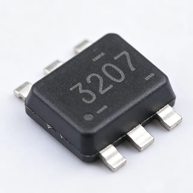
TPS563207DRLR - 3A 17V Synchronous Buck Converter | TI
料号: TPS563207DRLR ✓ 量产中| 数量 | 单价 | 小计 |
|---|---|---|
| 1 | $0.62 | $0.62 |
| 10 | $0.56 | $5.60 |
| 100 | $0.45 | $45.00 |
| 500 | $0.38 | $190.00 |
| 1,000 | $0.31 | $310.00 |
TPS563207DRLR 概述
A DC-DC switching regulator (step-down converter) converts a higher input voltage to a lower regulated output using power MOSFET switches, an inductor, and output capacitors. Synchronous buck converters replace the freewheeling diode with a second MOSFET for higher efficiency. Within the power-management IC hierarchy, the TPS563207 is a monolithic buck regulator with integrated high-side and low-side FETs.
Key features include D-CAP2 mode control for fast transient response and support of low-ESR output capacitors such as specialty polymer and ultra-low-ESR ceramic types. Fixed-frequency operation in Forced CCM (FCCM) mode maintains small output ripple even at light loads. The 3-A rating with integrated FETs minimizes external component count, and the tiny SOT-563 footprint suits dense PCB layouts. The device is specified from -40C to +125C junction temperature.
Internally, D-CAP2 control combines a wide-bandwidth error amplifier with an adaptive on-time generator, enabling near-constant frequency operation and quick response to load steps with minimal output capacitance. Internal compensation and soft-start reduce design effort and board area.
Typical applications include 5 V and 12 V rail point-of-load regulation for networking equipment, SSDs and storage, industrial PCs, FPGA/ASIC auxiliary rails, and consumer electronics. The 17-V maximum input covers 12-V buses with margin.
Design tip: choose the inductor value and output capacitors per the TI datasheet equations; FCCM mode favors low ripple, while the 0.806-V feedback reference supports low-voltage cores. Verify thermal performance, as the small DRL package dissipates heat mainly through the PCB.
直接替换替代料: TPS563207DRLR ——相同封装,引脚兼容。需要 PCB 改动的不同封装料号已排除。
本系列中的变体
可与以下型号直接替换的同系列型号: TPS563207DRLR (相同外形与封装尺寸) ——差异在于 Maximum Output Current, Output Voltage Range, Package, Input Voltage Range, Topology.
快速对比工具——选择替代料号进行并排对比:
TPS563207SDRLR
📋 参考替代料(不在目录中)
TPS563201DRLR
📋 参考替代料(不在目录中)
TPS563208DRLR
📋 参考替代料(不在目录中)
TPS563211DRLR
📋 参考替代料(不在目录中)
TPS563212DRLR
📋 参考替代料(不在目录中)
TPS56A207DRLR
📋 参考替代料(不在目录中)
TPS563207DRLR 最大额定值与电气特性
| 拓扑 | Synchronous Buck (Step-Down) |
| 输入电压范围 | 4.3 V to 17 V |
| 输出电压范围 | 0.806 V adjustable |
| 最大输出电流 | 3 A |
| Control Mode | D-CAP2 mode |
| Operating Mode | Forced CCM (FCCM) |
| 输出数量 | 1 |
| 输出类型 | Positive, Adjustable |
| Junction Temperature Range | -40C to +125C |
| 封装 | SOT-563 (DRL), 6-pin, 1.6 mm x 1.6 mm |
| 安装类型 | Surface Mount |
| FET Integration | Synchronous, integrated high-side and low-side MOSFETs |
| Supported Output Capacitors | Low-ESR ceramic and specialty polymer |
| RoHS 状态 | Compliant |
TPS563207DRLR 引脚配置
| 引脚 1 | EN — Enable pin, logic high enables the converter |
| 引脚 2 | GND — Ground reference |
| 引脚 3 | SW — Switch node, connect to power inductor |
| 引脚 4 | VIN — Input supply, 4.3 V to 17 V |
| 引脚 5 | FB — Feedback input for output voltage regulation |
| 引脚 6 | BOOT — Bootstrap for high-side gate driver, capacitor to SW |
典型应用
TPS563207DRLR 适用于 6 应用s: Networking Equipment Point-of-Load, SSD and Storage Systems, Industrial Automation Control, FPGA and ASIC Auxiliary Rails, Consumer Electronics Power, Battery-Powered and Portable Devices.
Networking Equipment Point-of-Load
The TPS563207DRLR suits 12-V bus powered networking switches, routers, and access points that need compact 3-A local rails for PHYs, MACs, and memory. Its 4.3-V to 17-V input accepts 12-V rails directly, and the 0.806-V adjustable output covers 1.0-V, 1.2-V, 1.8-V, and 3.3-V needs via resistor dividers. D-CAP2 control delivers fast transient response during bursty packet traffic, while FCCM mode keeps ripple low at light loads. The 1.6-mm x 1.6-mm SOT-563 package fits dense port-side layouts.
推荐
SSD and Storage Systems
Solid-state drives and storage controllers require tiny, efficient point-of-load converters; the TPS563207DRLR answers with a 1.6-mm x 1.6-mm SOT-563 footprint and integrated synchronous FETs rated 3 A. The 12-V input matches SATA/NVMe drive power, and D-CAP2 mode supports ultra-low-ESR ceramic output capacitors, minimizing BOM area. FCCM operation keeps output ripple small during idle and active states, protecting noise-sensitive controller and NAND rails. Its -40C to +125C junction range covers drive thermal environments.
推荐
Industrial Automation Control
In factory automation, PLC I/O modules and sensor interfaces often distribute 12 V or 24 V (with pre-regulation) and need robust local step-down conversion. The TPS563207DRLR provides 3 A from a 4.3-V to 17-V input with -40C to +125C junction specification, suiting harsh cabinet environments. D-CAP2 control tolerates low-ESR ceramic capacitors, improving reliability where electrolytics would age. The simple external component count of typically an inductor plus input/output capacitors accelerates design cycles for industrial OEMs.
推荐
FPGA and ASIC Auxiliary Rails
FPGA and ASIC designs need multiple auxiliary rails (1.0 V to 3.3 V) with fast load-step response for I/O banks, transceivers, and configuration logic. The TPS563207DRLR adjustable output from 0.806 V and D-CAP2 transient performance handle switching surges, while the 3-A rating covers mid-current rails. FCCM mode maintains predictable ripple for analog-heavy auxiliary supplies. Small size allows the converter to sit close to the load, reducing parasitic inductance and improving transient response.
推荐
Consumer Electronics Power
Set-top boxes, smart displays, and consumer appliances use 12-V adapters and need low-cost, small-footprint buck conversion. The TPS563207DRLR offers competitive sub-$0.70 unit pricing as of 2026-08-29, a 6-pin SOT-563 package, and minimal external parts, reducing BOM cost and board area. Its FCCM mode yields low output ripple for sensitive audio/video circuitry, while the 3-A capability covers HDMI, SoC, and wireless module rails with margin. The -40C to +125C junction spec adds robustness.
推荐
Battery-Powered and Portable Devices
Portable instruments and battery packs with multi-cell stacks (4S-3S lithium ranges near 12-17 V) benefit from the TPS563207DRLR 17-V maximum input. The synchronous architecture achieves high efficiency at the 3-A level, extending battery runtime versus nonsynchronous designs. D-CAP2 mode maintains stability with compact ceramic output capacitors, and the tiny SOT-563 package suits handheld enclosures. Designers should manage light-load behavior: FCCM trades standby efficiency for low ripple.
推荐
推荐产品汇总
工程参考数据: TPS563207DRLR ——对比、设计指导和合规信息。
选型指南
与替代料对比
| 参数 | 本产品 | TPS563207SDRLR | TPS563201DRLR | TPS563211DRLR |
|---|---|---|---|---|
| Package | SOT-563 (DRL) 1.6 mm x 1.6 mm | SOT-563 (DRL) - same | SOT-563 (DRL) - same | SOT-563 (DRL) - same |
| Brand | Texas Instruments | Texas Instruments | Texas Instruments | Texas Instruments |
| Input Voltage Range | 4.3 V to 17 V | 4.3 V to 17 V | 4.5 V to 17 V | 4.5 V to 17 V |
| Output Current | 3 A | 3 A | 3 A | 3 A |
| Control Mode | D-CAP2, FCCM | D-CAP2, FCCM | D-CAP2, eco-mode (DCM) | D-CAP2, eco-mode |
| Light-Load Ripple | Low (FCCM fixed frequency) | Low (FCCM) | Higher ripple, higher efficiency at light load | Higher ripple, higher efficiency at light load |
| Junction Temperature Range | -40C to +125C | -40C to +125C | -40C to +125C | -40C to +125C |
关键差异点
- Forced-CCM operation for low light-load ripple (对比 TPS563201DRLR)
- Ultra-small 3-A footprint (对比 TPS560200DBVR)
- Lowest feedback reference in family enables low-voltage rails (对比 TPS563207SDRLR)
设计说明
Keep the power loop (VIN capacitor, integrated FETs, SW pin, inductor, output capacitor) as tight as possible. Place a 10-uF ceramic input capacitor within 2 mm of VIN and GND, and the output capacitor close to the inductor. Connect the BOOT capacitor (0.1 uF typical) directly between BOOT and SW. Because the SOT-563 package dissipates heat through the PCB, use at least a small ground plane and thermal vias under the GND pin; per TI datasheet layout guidelines, the DRL package theta_JA depends heavily on copper area.
Select the inductor using the TI datasheet equations, typically 1.5 uH to 4.7 uH for common 1.0-V to 3.3-V outputs. Verify peak current rating exceeds the switch current limit plus margin, and check RMS ripple current. Use X7R/X5R ceramic output capacitors with DC-bias derating accounted for - effective capacitance can drop 50% at rated voltage, affecting stability of the D-CAP2 loop.
Do not exceed the 17-V absolute input rating; 24-V industrial buses require a front-end regulator. Ensure EN is not left floating above its absolute maximum if driven from a divider. The FCCM mode keeps switching at light load - this lowers ripple but raises standby quiescent draw; if battery life dominates, consider eco-mode family members like TPS563201 instead. Verify FB divider current stays low to avoid draining low-power rails.
合规信息
RoHS compliance per DigiKey product listing. REACH and halogen-free status not stated in provided data.







