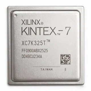
XC7K410T-L2FFG900E - 406,720 Logic Cells Kintex-7 FPGA | AMD
MPN: XC7K410T-L2FFG900E ✓ Hoạt độngXC7K410T-L2FFG900E Tóm tắt
An FPGA is a programmable semiconductor in which the logic, interconnects, and digital signal processing blocks are configured by a bitstream after manufacture. Kintex-7 devices belong to the FPGA and CPLD product hierarchy, combining configurable logic, block RAM, DSP slices, high-speed I/O, and clock-management resources in one integrated device. This combination allows designers to implement parallel processing, protocol bridging, control systems, video and communications infrastructure, and embedded signal processing without using multiple fixed-function ASICs.
Key resources include 406,720 logic cells, 500 I/O, 293,06880 block RAM bits, and support for the Kintex-7 family's high-performance connectivity and signal-processing capabilities. The 900-ball FCBGA package provides a large pin count for high-bandwidth designs, while the -2 speed grade identifies the device's performance class. The FFG900 package is intended for designs that need extensive I/O and package-level routing flexibility.
The Kintex-7 architecture is suited to systems requiring deterministic programmable logic alongside parallel data processing. Available resources can support network interface functions, high-throughput data acquisition, industrial control, test equipment, communications infrastructure, embedded processing, and signal-processing subsystems. The large logic and memory capacity also allows multiple subsystems to be integrated on one FPGA, reducing board-level interconnects and simplifying synchronization among processing blocks.
AMD's Kintex-7 documentation describes the device family as supporting mainstream connectivity standards such as PCIe Gen3 and 10 Gigabit Ethernet, as well as a high ratio of DSP resources for parallel arithmetic workloads. These capabilities make the XC7K410T-L2FFG900E relevant to communication backplanes, protocol converters, test systems, high-speed data acquisition, and industrial equipment that require flexible logic and serial connectivity.
When laying out the PCB, use the AMD package pinout files and follow the 900-BBGA FCBGA escape-routing and power-distribution guidance for the selected Kintex-7 device. Decoupling, layer transitions, differential-pair routing, and package-ball assignment should be reviewed against the current AMD design guidance. Because this part has a large pin count and substantial programmable capability, power planning, thermal design, and signal-integrity verification are as important as the logical design itself.
This product page summarizes the manufacturer and distributor information for the XC7K410T-L2FFG900E, including its key package and resource characteristics, practical application positioning, design considerations, and qualified replacement analysis. Use the current AMD datasheet and package files as the controlling references for electrical limits, pin assignments, configuration, and PCB implementation.
Bộ thay thế dễ dàng lắp đặt cho XC7K410T-L2FFG900E — cùng gói, chân-to-chân tương thích. Các bộ phận yêu cầu hàn PCB bị loại trừ.
Các biến thể trong loạt này
Các mẫu cùng loạt có thể lắp đặt dễ dàng tương thích với XC7K410T-L2FFG900E (cùng hình factor và footprint) — khác nhau ở Logic Cells, Block RAM, DSP Slices, Package.
XC7K410T-2FFG900I
✅ Drop-InLiên hệ để biết giá
Xem tài liệu →XC7K410T-2FFG900C
✅ Drop-InLiên hệ để biết giá
Xem tài liệu →XC7K410T-L2FFG900E Tỷ lệ tối đa & tính chất điện
| Device Type | Kintex-7 FPGA |
| Logic Cells | 406,720 cells |
| I/O Count | 500 I/O |
| Embedded Block RAM | 29,306,880 bits |
| Technology Process | 28 nm |
| Speed Grade | -2 |
| Package Type | 900-BBGA, FCBGA |
| Package Pin Count | 900 balls |
| Kiểu lắp đặt | Surface Mount |
| Core Voltage | 0.9 V |
| Supported High-Speed Interfaces | PCIe Gen3 and 10 Gigabit Ethernet device-family capabilities |
| Trạng thái vòng đời | Active |
Hướng dẫn cấu hình chân XC7K410T-L2FFG900E 900 balls
Cấu hình chân cho XC7K410T-L2FFG900E (900 balls gói). IC số này bao gồm chân GPIO, giao diện truyền thông (UART, SPI, I2C) và chân nguồn. Tham khảo tài liệu thông số kỹ thuật của nhà sản xuất để biết các chức năng chân thay thế và tùy chọn cấu hình. Cực kỳ quan trọng cho thiết kế hệ thống tích hợp và lập trình PCB.

Không có dữ liệu chân cụ thể sẵn có cho XC7K410T-L2FFG900E.
Tham khảo: tài liệu kỹ thuật cho cấu hình chân đầy đủ.
Ứng dụng tiêu biểu
XC7K410T-L2FFG900E phù hợp cho 6 Áp dụngs: PCIe Gen3 Interface Cards, 10 Gigabit Ethernet Network Equipment, Industrial Control and Automation, High-Throughput Data Acquisition, Test and Measurement Instrumentation, Embedded Signal Processing.
PCIe Gen3 Interface Cards
The XC7K410T-L2FFG900E is suitable for PCIe Gen3 interface cards because the Kintex-7 family is positioned for high-performance connectivity and combines 406,720 logic cells with 500 I/O. A designer can place protocol logic, DMA engines, data buffers, clocking, and monitoring functions in one programmable device. The 900-BBGA FCBGA package also provides a large I/O and power-delivery resource for high-speed escape routing. Implementation still requires compliant reference-controlled routing, proper transceiver or I/O selection, and complete timing closure. Use the AMD Kintex-7 design guidance and package files to verify ball assignments, reference planes, and thermal performance before fabrication.
Được đề xuất
10 Gigabit Ethernet Network Equipment
The XC7K410T-L2FFG900E fits network equipment requiring substantial parallel logic, block RAM, and programmable I/O for 10 Gigabit Ethernet-class designs. Its 406,720 logic cells can support packet processing, buffering, statistics, traffic management, and control-plane functions, while 29,306,880 block RAM bits provide storage for packet queues and lookup structures. The -2 speed grade supports performance-oriented designs, and the 900-BBGA package offers extensive routing and power connectivity. Deployment requires careful clocking, SerDes configuration, signal-integrity analysis, and thermal planning under sustained network traffic.
Được đề xuất
Industrial Control and Automation
The XC7K410T-L2FFG900E can be used in industrial control and automation systems where deterministic parallel logic, programmable I/O, and local data processing are valuable. The large logic-cell count allows motion control, sensor aggregation, machine vision preprocessing, safety-adjacent monitoring, and protocol conversion to coexist in one FPGA. Its 500 I/O provide capacity for digital and differential interfaces, while block RAM supports buffering and time-domain processing. The 900-BBGA FCBGA package is appropriate for multilayer boards but demands disciplined power distribution, decoupling, thermal analysis, and long-term component-availability review for production equipment.
Được đề xuất
High-Throughput Data Acquisition
The XC7K410T-L2FFG900E is appropriate for high-throughput data-acquisition systems that must combine parallel conversion control, digital filtering, buffering, and real-time processing. The 406,720 logic cells provide substantial capacity for acquisition pipelines and trigger logic, while 29,306,880 block RAM bits can support sample storage and rolling buffers. The 500-I/O capability supports parallel data interfaces and control signals, and the -2 speed grade targets higher-performance processing. In practice, engineers should use AMD timing and power tools to establish achievable data rates, then verify impedance-controlled routing, clock jitter, grounding, and thermal rise on the assembled board.
Được đề xuất
Test and Measurement Instrumentation
The XC7K410T-L2FFG900E fits test and measurement instruments requiring programmable logic, high I/O density, and flexible signal processing. A single device can implement pattern generation, acquisition pipelines, real-time analysis, timing control, and instrument-control interfaces. The 406,720 logic cells and 29,306,880 block RAM bits allow substantial test-vector and sample buffering, while 500 I/O simplifies integration with external converters, memories, and clock sources. The 900-BBGA FCBGA package offers the pin density needed for parallel instrumentation but requires a multilayer PCB strategy, continuous power-plane design, and detailed thermal verification around the FPGA.
Được đề xuất
Embedded Signal Processing
The XC7K410T-L2FFG900E supports embedded signal-processing systems that combine configurable logic, DSP slices, block RAM, and high-speed serial connectivity. Parallel filters, transforms, modulation functions, correlation engines, and adaptive-control loops can be implemented in programmable hardware, allowing deterministic latency and reconfigurable behavior. The device's 406,720 logic cells provide integration headroom beyond one processing pipeline, while 29,306,880 block RAM bits support coefficient storage and sample histories. Designers should establish numerical performance and resource utilization in the FPGA toolchain, then account for clock uncertainty, package power delivery, heat dissipation, and high-speed signal-integrity behavior.
Được đề xuất
Tóm tắt các sản phẩm được đề xuất
Dữ liệu tham khảo kỹ thuật cho XC7K410T-L2FFG900E — so sánh, hướng dẫn thiết kế và thông tin tuân thủ.
Hướng dẫn chọn lựa
So sánh với các sản phẩm thay thế
| Tham số | Sản phẩm này | XC7K410T-2FFG900I | XC7K410T-2FFG900C |
|---|---|---|---|
| Brand | AMD | AMD | AMD |
| Package | 900-BBGA, FCBGA | 900-BBGA, FCBGA | 900-BBGA, FCBGA |
| FPGA Family | Kintex-7 | Kintex-7 | Kintex-7 |
| Logic Cells | 406,720 cells | 406,720 cells | 406,720 cells |
| I/O Count | 500 I/O | 500 I/O | 500 I/O |
| Embedded Block RAM | 29,306,880 bits | 29,306,880 bits | 29,306,880 bits |
| Technology Process | 28 nm | 28 nm | 28 nm |
| Speed Grade | -2 | -2 | -2 |
| Core Voltage | 0.9 V | 0.9 V | 0.9 V |
| Ordering Suffix | L2FFG900E | 2FFG900I | 2FFG900C |
| High-Speed Interface Support | Kintex-7 family supports PCIe Gen3 and 10 Gigabit Ethernet capabilities | Kintex-7 family supports PCIe Gen3 and 10 Gigabit Ethernet capabilities | Kintex-7 family supports PCIe Gen3 and 10 Gigabit Ethernet capabilities |
Bảo phân biệt quan trọng
- High logic and memory density in a 900-ball package (vsXC7K410T-2FFG900I)
- Same-package alternative with identical listed resource class (vsXC7K410T-2FFG900C)
- Kintex-7 connectivity and DSP positioning (vsXC7K410T-2FFG900I)
Ghi chú thiết kế
Start the PCB layout with the AMD 900-BBGA FCBGA package pinout and ball-assignment files, then validate the component library against the exact ordering code. Route configuration signals, clock inputs, reset, and high-speed interfaces according to the AMD Kintex-7 PCB guidelines. Use short, direct connections for bypass capacitors and a continuous power-distribution structure, and avoid placing sensitive high-speed routes adjacent to noisy switching or power-conversion nodes.
Plan the supply network for the device's worst-case utilization and I/O activity rather than a nominal idle condition. Decoupling should follow the manufacturer recommendation for each power rail and be distributed across the package footprint rather than concentrated at one edge. Validate voltage sequencing, current capacity, connector and plane resistance, and the transient response in the assembled board. Use Vivado power analysis to estimate activity-dependent consumption and include it in the board thermal design.
Treat the 900-BBGA FCBGA as a high-speed, high-pin-count package. Maintain continuous reference planes beneath the device where the design rules permit, control impedance on high-speed nets, and minimize layer transitions through the BGA escape region. Match clock and data lengths according to the selected interface specification, and reserve adequate room for debugging access, programming, boundary scan, and production test. Review escape-routing topology against the current AMD package guidance before releasing the fabrication files.
Thermal performance depends on device utilization, the selected speed grade, local power distribution, airflow, and PCB copper. Begin with the AMD power estimate for the final configuration, add board-environment effects, and verify that the junction-temperature limit remains satisfied at the highest expected ambient temperature. A large FCBGA benefits from a properly designed multilayer PCB, but thermal vias, copper spreading, and enclosure airflow should be evaluated as a system rather than added only after failure symptoms appear.
Do not treat a matching package name as proof that two Kintex-7 ordering codes are drop-in replacements. The target uses the L2FFG900E suffix, while the identified alternatives use different suffixes such as 2FFG900I and 2FFG900C. Before approving a substitution, compare the complete AMD ordering information, temperature range, qualification, lifecycle status, configuration behavior, and bitstream or design-tool requirements. Validate the replacement with the production test plan as well as the engineering prototype.
Thông tin tuân thủ
Compliance fields require confirmation from the current AMD product documentation or material declaration for the exact ordering code.