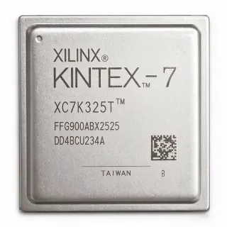
XC7K410T-2FFG900C - Kintex-7 FPGA 406K Logic Cells | AMD
MPN: XC7K410T-2FFG900C ✓ Active| Qty | Unit Price | Extended |
|---|---|---|
| 1 | $1295 | $1,295.00 |
| 10 | $1198 | $11,980.00 |
| 100 | $1099 | $109,900.00 |
| 500 | $1049 | $524,500.00 |
| 1,000 | $999 | $999,000.00 |
XC7K410T-2FFG900C Overview
An FPGA (Field Programmable Gate Array) is an integrated circuit that can be configured by the customer or designer after manufacturing. Unlike fixed-function ASICs, FPGAs contain programmable logic blocks, configurable interconnects, and embedded memory that allow the hardware to be reprogrammed to implement arbitrary digital logic functions. FPGAs sit within the broader hierarchy of programmable logic devices (PLDs), which range from simple CPLDs to massive data center accelerators. The Kintex-7 family specifically targets the balance of price, performance, and power at 28nm, offering high DSP ratios and support for mainstream standards like PCIe Gen3 and 10 Gigabit Ethernet.
Key features of the XC7K410T-2FFG900C include 1,540 DSP slices for high-throughput digital signal processing, 500 user I/O pins supporting multiple I/O standards, and 29,306,880 bits of block RAM. The device also integrates hardened memory controllers, high-speed serial transceivers, and clock management tiles (MMCM and PLL) for robust timing. The -2 speed grade provides a balance between performance and power consumption, with a maximum clock frequency of 1286 MHz for internal logic.
Architecturally, the Kintex-7 family uses a unified 7 series architecture with configurable logic blocks (CLBs), block RAM, and DSP48E1 slices. The 28nm high-k metal gate (HKMG) process enables high logic density while maintaining reasonable power dissipation. The device supports partial reconfiguration, allowing dynamic updates to specific logic regions without halting the entire system.
Typical applications include high-performance computing, aerospace and defense signal processing, medical imaging, and wired/wireless communications infrastructure. The 900-ball FCBGA package provides excellent thermal and electrical characteristics for high-speed designs.
When designing with this FPGA, careful attention must be paid to power supply decoupling and thermal management. The device requires multiple voltage rails (VCCINT, VCCAUX, VCCO) with proper sequencing, and the FCBGA package benefits from a thermal solution for high-utilization designs.
Drop-in alternatives for XC7K410T-2FFG900C — same package, pin-to-pin compatible. Different-package parts requiring PCB rework are excluded.
Variants in this series
Same-series models that are drop-in compatible with XC7K410T-2FFG900C (same form factor and footprint) — differing in Package, Block RAM, Clock Management, DSP Slices, Logic Cells.
Quick Comparison Tool — Select alternative parts for side-by-side comparison:
XC7K410T-1FFG900C
✅ Drop-In📋 Reference alternative (not in catalog)
XC7K325T-2FFG900C
✅ Drop-In✓ In Stock
$1590 / Unit
View Datasheet →XC7K480T-2FFG900C
✅ Drop-In ⚠️ Specs Unverified📋 Reference alternative (not in catalog)
XC7K420T-2FFG900C
✅ Drop-In ⚠️ Specs Unverified📋 Reference alternative (not in catalog)
XC7K160T-2FFG900C
✅ Drop-In ⚠️ Specs Unverified📋 Reference alternative (not in catalog)
XC7K410T-2FFG900C Maximum Ratings & Electrical Characteristics
| Family | Kintex-7 |
| Logic Cells | 406720 |
| Block RAM | 29306880 bits |
| DSP Slices | 1540 |
| User I/O | 500 |
| CLBs | 31775 |
| Maximum Clock Frequency | 1286 MHz |
| Technology | 28nm |
| Core Supply Voltage | 1V |
| Package | 900-BBGA, FCBGA |
| Mounting Type | Surface Mount |
| Speed Grade | -2 |
| Operating Temperature | 0C to +85C (Commercial) |
| RoHS Status | Compliant |
XC7K410T-2FFG900C Pin Configuration
| Pin A1 | IO_L1P_T0 — User I/O bank 0, differential pair P |
| Pin A2 | IO_L1N_T0 — User I/O bank 0, differential pair N |
| Pin B1 | VCCINT — Core logic supply voltage (1V) |
| Pin B2 | GND — Ground |
| Pin C1 | IO_L2P_T0 — User I/O bank 0, differential pair P |
| Pin C2 | IO_L2N_T0 — User I/O bank 0, differential pair N |
| Pin D1 | VCCAUX — Auxiliary supply voltage (1.8V) |
| Pin D2 | GND — Ground |
| Pin E1 | IO_L3P_T0 — User I/O bank 0, differential pair P |
| Pin E2 | IO_L3N_T0 — User I/O bank 0, differential pair N |
| Pin F1 | VCCO_0 — I/O bank 0 supply voltage |
| Pin F2 | GND — Ground |
Typical Applications
XC7K410T-2FFG900C is suitable for 6 applications: High-Performance Computing, Aerospace and Defense Signal Processing, Medical Imaging, Wired and Wireless Communications, Test and Measurement Equipment, Data Center Acceleration.
High-Performance Computing
The XC7K410T-2FFG900C excels in high-performance computing applications such as data acceleration and scientific simulation. With 406,720 logic cells and 1,540 DSP slices, it can implement complex parallel processing algorithms. The 500 user I/O pins enable high-bandwidth data movement, while the 28nm process balances performance and power. Engineers can use it for custom accelerators in financial modeling, genomics, and signal processing, where its reconfigurability allows algorithm updates without hardware changes.
Recommended
Aerospace and Defense Signal Processing
In aerospace and defense, the XC7K410T-2FFG900C is used for radar, electronic warfare, and secure communications. Its high DSP slice count (1,540) supports fast Fourier transforms and beamforming algorithms. The 900-ball FCBGA package provides reliable operation in harsh environments, and the device's reconfigurability allows field updates for evolving threats. The 500 I/O pins interface with high-speed ADCs and DACs, while the 28nm technology ensures low power for airborne platforms.
Recommended
Medical Imaging
The XC7K410T-2FFG900C is ideal for medical imaging systems like CT scanners and ultrasound machines. Its 406,720 logic cells handle image reconstruction algorithms, while the 29,306,880 bits of block RAM store intermediate data. The 1,540 DSP slices accelerate filtering and enhancement operations. The device's high I/O count (500) connects to multiple sensor arrays, and its reliability meets medical device standards. The 28nm process ensures efficient power consumption for portable systems.
Recommended
Wired and Wireless Communications
For communications infrastructure, the XC7K410T-2FFG900C supports baseband processing in 5G and LTE systems. Its high logic density implements complex modulation schemes, while the 500 I/O pins interface with RF transceivers and Ethernet PHYs. The device supports PCIe Gen3 and 10 Gigabit Ethernet, enabling high-speed backhaul. The 28nm process provides a balance of performance and power, making it suitable for remote radio heads and central units.
Recommended
Test and Measurement Equipment
The XC7K410T-2FFG900C is used in oscilloscopes, logic analyzers, and signal generators. Its 406,720 logic cells implement high-speed data acquisition and triggering logic. The 1,540 DSP slices perform real-time signal analysis, while the 500 I/O pins connect to high-speed ADCs and DACs. The device's reconfigurability allows firmware updates to add new measurement features. The 900-ball FCBGA package supports dense PCB layouts for compact instruments.
Recommended
Data Center Acceleration
In data centers, the XC7K410T-2FFG900C accelerates workloads like video transcoding, database queries, and AI inference. Its 406,720 logic cells implement custom accelerators, while the 1,540 DSP slices handle matrix operations. The device supports PCIe Gen3 for host connectivity, and the 500 I/O pins enable high-bandwidth memory interfaces. The 28nm process offers a cost-effective balance of performance and power for rack-scale deployments.
Recommended
Recommended Products Summary
Engineering reference data for XC7K410T-2FFG900C — comparison, design guidance, and compliance information.
Selection Guide
Comparison with Alternatives
| Parameter | This Product | XC7K410T-1FFG900C | XC7K325T-2FFG900C | XC7K480T-2FFG900C |
|---|---|---|---|---|
| Package | 900-BBGA, FCBGA | 900-BBGA, FCBGA - same | 900-BBGA, FCBGA - same | 900-BBGA, FCBGA - same |
| Brand | AMD | AMD | AMD | AMD |
| Logic Cells | 406720 | 406720 | 326080 | 477760 |
| Block RAM (bits) | 29306880 | 29306880 | 16025760 | 38246400 |
| DSP Slices | 1540 | 1540 | 840 | 1920 |
| User I/O | 500 | 500 | 500 | 500 |
| Speed Grade | -2 | -1 | -2 | -2 |
Key Differentiators
- Higher logic density than XC7K325T (vs XC7K325T-2FFG900C)
- Faster speed grade than XC7K410T-1FFG900C (vs XC7K410T-1FFG900C)
- More block RAM than XC7K325T (vs XC7K325T-2FFG900C)
Design Notes
The XC7K410T-2FFG900C requires multiple power rails: VCCINT (1V), VCCAUX (1.8V), and VCCO (varies by I/O bank). Use a dedicated power management solution with proper sequencing. According to AMD's 7 Series FPGAs datasheet, VCCINT must be applied before or simultaneously with VCCAUX. Decouple each rail with a combination of bulk and ceramic capacitors placed close to the FPGA pins.
The 900-ball FCBGA package has a thermal resistance that requires careful management. For high-utilization designs, use a heatsink or active cooling. The maximum junction temperature is 85C for commercial grade. Calculate power dissipation using AMD's Power Estimator tool and ensure adequate airflow in the enclosure.
For high-speed signals, use controlled impedance traces and minimize stub lengths. The FFG900 package has a 1.0mm ball pitch, requiring fine-pitch PCB fabrication. Follow AMD's PCB design guidelines in UG483 for routing and via placement. Use ground planes under the FPGA to reduce noise and improve signal integrity.
Compliance Information
RoHS compliance indicated by distributor listings. AEC-Q100 not applicable for FPGA. Other compliance data not specified in provided sources.