產品(42,000+)

OPA1688 - 36V 10MHz Low Noise Audio Op Amp | TI
OPA1688ID

OPA1688 - 36V 10MHz Low Noise Audio Op Amp | TI

The Texas Instruments OPA1688ID is a 36-V, single-supply, low-noise SoundPlus audio operational amplifier operating on supplies from 4.5 V (±2.25 V) to 36 V (±18 V), with 10-MHz bandwidth, rail-to-rail output, and low distortion. It is offered in SOIC-8 and WSON-8 packages. An operational amplifier (op amp) is a high-gain voltage amplifier with differential inputs and a single-ended output, fundamental to analog signal conditioning, filtering, and amplification. The OPA1688 belongs to the SoundPlus family of audio op amps, optimized for low noise, low distortion, and high output drive within the broader linear amplifier category used across audio, instrumentation, and communication systems. Key features include 4.5 nV/√Hz input voltage noise, an 8 V/µs slew rate, and low quiescent current of 1.5 mA per channel. Excellent capacitive load stability allows direct drive of up to 1000 pF without oscillation, and ±75 mA output current enables direct headphone drive. The rail-to-rail output (RRO) stage maximizes dynamic range in single-supply designs. Technically, the OPA1688 uses a complementary bipolar input stage with laser-trimmed input offset voltage of 0.5 mV (typical). The wide supply range supports both battery-powered and industrial systems, and the -40C to +85C operating range ensures reliability in demanding environments. THD+N of 0.00005% at 1 kHz and high PSRR preserve signal fidelity in high-fidelity audio paths. Typical applications include headphone amplifiers, audio DAC output buffers, active filters, and professional audio mixing consoles. High output current and capacitive load stability make it especially suited to direct headphone drive, while low noise and distortion preserve audio integrity in portable devices where 1.5 mA quiescent current extends battery life. Design tip: decouple supply pins with 0.1 µF ceramic capacitors placed close to the device, keep feedback paths short to minimize parasitic capacitance, and use an isolation resistor for capacitive loads beyond 1000 pF. Pricing references are as of 2026-08-30.

詢價 聯絡我們
OPA170AIDBVT - 36V, 1.2MHz, Low-Power Op Amp | Texas Instruments
OPA170AIDBVT

OPA170AIDBVT - 36V, 1.2MHz, Low-Power Op Amp | Texas Instruments

The Texas Instruments OPA170AIDBVT is a single-channel, 36-V, 1.2-MHz, low-power operational amplifier (op amp) in a 5-pin SOT-23 (DBV) package, offering rail-to-rail output swing and excellent DC precision for cost-sensitive general-purpose applications. According to the manufacturer datasheet, the device operates on supplies from 2.7 V (±1.35 V) to 36 V (±18 V), supports 1.2 MHz unity-gain bandwidth, and delivers low offset voltage with low quiescent current. What is a low-power operational amplifier? A low-power op amp is a class of analog amplifier IC designed to operate on single or dual supplies while consuming minimal quiescent current, enabling battery-powered and energy-efficient designs. Low-power op amps sit within the broader operational amplifier family, which belongs to linear ICs and the signal-conditioning product hierarchy. They balance bandwidth, offset, and noise against supply current, making them ideal for always-on sensor interfaces and portable instrumentation. Key features include rail-to-rail output (RRO), an enable/shutdown pin for power sequencing, low offset voltage, low drift over temperature, and 1.2 MHz gain-bandwidth product. The device also provides ESD protection on the inputs/outputs and is specified over the -40 °C to +125 °C industrial temperature range. The 5-pin SOT-23 footprint enables extremely compact PCB designs for space-constrained analog front ends. Architecturally, the OPA170 uses a bipolar input stage with CMOS output stages for rail-to-rail swing, and the family (OPA170/OPA2170/OPA4170) shares identical specifications across single, dual, and quad versions for easy design portability. The combination of 36 V tolerance, low quiescent current, and small packaging positions the OPA170 as a strong fit for industrial sensors, transducer signal conditioning, and active filtering. Typical applications include current sensing in power management, transducer amplifiers for pressure/flow sensors, active filters, test equipment input buffers, and general-purpose signal conditioning for industrial control and battery-powered systems. Designers choose the OPA170 family when they need robust 36 V tolerance, low power, and rail-to-rail output in a tiny footprint. When designing with this device, place a 0.1 µF decoupling capacitor as close as possible to the power-supply pin and ensure input common-mode range is respected. The shutdown/enable pin allows direct power-rail control in low-power duty-cycled applications. This page synthesizes verified distributor pricing, parametric drop-in alternatives, and practical design guidance not found in the manufacturer datasheet, all anchored to the official TI OPA170 datasheet as of 2026-10-09.

詢價 聯絡我們
OPA171AIDRLT - 36V 3MHz Single Op Amp | Texas Instruments
OPA171AIDRLT

OPA171AIDRLT - 36V 3MHz Single Op Amp | Texas Instruments

The Texas Instruments OPA171AIDRLT is a single-channel, 36V, 3MHz, low-power operational amplifier (op amp) in a 5-pin SOT-553 (DRL) micropackage with rail-to-rail output (RRO). It is part of the OPAx171 family, which shares identical AC and DC specifications across single, dual, and quad versions for maximum design flexibility. The device operates from a single supply of 2.7V to 36V (or dual ±1.35V to ±18V), drawing only 475 µA of quiescent current per channel while delivering 3 MHz of gain-bandwidth product and 1.5 V/µs slew rate. An operational amplifier (op amp) is a high-gain DC-coupled electronic voltage amplifier with differential inputs and a single-ended output, used as a foundational building block in analog signal chains. Op amps sit inside the broader hierarchy of linear integrated circuits (ICs) -> amplifiers -> operational amplifiers, and are commonly classified by supply range, bandwidth, power, and noise. The OPA171 is targeted at low-power, single-supply general-purpose applications where a wide supply range (up to 36V) and rail-to-rail output swing are required - it is NOT a precision or low-noise audio op amp, but rather a general-purpose workhorse for industrial and consumer designs. Key features of the OPA171AIDRLT include 3 MHz GBW, 1.5 V/µs slew rate, 475 µA quiescent current, 36 V supply tolerance, rail-to-rail output swing, ±2 mV typical input offset voltage, and internal RF/EMI filtering on the inputs. The SOT-553 (DRL) package is a low-profile (~0.5 mm) surface-mount micropackage suitable for space-constrained PCB designs. The OPAx171 family delivers low offset, low drift, low quiescent current, and 3 MHz bandwidth simultaneously - a combination rare in this supply-voltage class. Architecturally, the OPA171 uses a CMOS input stage that allows true rail-to-rail input common-mode range (no input phase reversal), paired with a class AB output stage capable of rail-to-rail swing. Internal EMI/RFI rejection filters on the input pins suppress high-frequency interference, simplifying compliance in industrial environments. The device is also specified over the -40°C to +125°C automotive and industrial temperature range. Typical applications include building automation sensor conditioning, battery-powered industrial transmitters, low-side current sensing, active filters, transducer drivers, and general-purpose signal buffering in 4-20 mA loops, PLC analog input modules, and portable instrumentation. The wide supply range (2.7V-36V) makes it well-suited to 5V USB-powered systems and 24V industrial bus rails from the same part. When designing with this op amp, observe that the input common-mode range extends to both rails but the input offset voltage degrades near the rails (CMOS input stage). Output is rail-to-rail but the output swing spec is typically within 50 mV of either rail at light loads. Decouple the supply pin with at least 0.1 µF X7R ceramic placed within 5 mm of the pin to ensure stability and PSRR performance. This page synthesizes DigiKey/Mouser distributor pricing, drop-in SOT-553 alternatives, and PCB design notes not aggregated on the manufacturer's product page.

詢價 聯絡我們
OPA172ID - 36V, 10MHz Rail-to-Rail Op Amp | Texas Instruments
OPA172ID

OPA172ID - 36V, 10MHz Rail-to-Rail Op Amp | Texas Instruments

The Texas Instruments OPA172ID is a single, 36 V, 10 MHz, low-power, rail-to-rail operational amplifier with rail-to-rail output in an 8-pin SOIC package. It supports a +4.5 V to +36 V supply range, equivalent to ±2.25 V to ±18 V, and combines a low 7 nV/√Hz noise density with a low input bias current of ±8 pA. These characteristics make it suitable for precision signal-chain and industrial measurement systems requiring low-noise amplification from relatively high-voltage supplies. An operational amplifier, commonly called an op amp, is a high-gain differential-input active device used to amplify voltage differences. The OPA172 belongs to the high-voltage CMOS operational-amplifier family, combining an amplifier core, input protection, bias compensation, and output-stage drive in one package. Its rail-to-rail output can approach the supply rails, improving output swing in single-supply systems where conventional amplifier designs may leave less usable voltage range. The OPA172ID provides a gain-bandwidth product of 10 MHz and an input offset voltage of ±0.2 mV. Input offset drift is limited to ±0.3 μV/°C, helping maintain accuracy as operating temperature changes. Quiescent current is 1.6 mA per amplifier, while the low input bias current supports high-impedance sources. The 7 nV/√Hz input-noise specification is particularly useful when the amplifier must preserve small signals rather than add substantial broadband noise. Operation from a single +4.5 V supply or from split supplies up to ±18 V gives designers flexibility around industrial, instrumentation, audio, and control circuits. Rail-to-rail output behavior supports low-voltage signal conditioning without requiring a separate negative supply. Designers should still verify output swing under load, input common-mode range, stability with the selected feedback network, and the absolute maximum input-current limit of 10 mA described in the manufacturer datasheet. Typical uses include sensor-signal conditioning, current-loop interfaces, precision buffers, audio output stages, industrial acquisition systems, and low-noise analog measurement chains. The single-amplifier configuration in the 8-pin SOIC package also simplifies designs that need one high-voltage amplifier rather than a dual or quad device. The low bias current is useful when the source impedance is high enough that input leakage would otherwise create a meaningful voltage error. A practical design should begin with the manufacturer datasheet pin configuration and typical application circuits. Keep sensitive input and feedback routes short, provide stable decoupling close to the supply pins, and verify amplifier stability for the intended capacitive loading. Avoid allowing input voltage to exceed the supply rails because excess input current can flow during abnormal operating conditions, and keep the input current below the recommended 10 mA limit. This page combines the OPA172ID operating limits, package details, application guidance, drop-in alternatives, and engineering trade-offs into one practical reference for high-voltage analog design. It also distinguishes direct pin-compatible choices from related family members so that replacement decisions are based on voltage range, bandwidth, noise, bias current, and output capability rather than package similarity alone.

詢價 聯絡我們
OPA177FP - Precision Low-Noise Op Amp | Texas Instruments
OPA177FP

OPA177FP - Precision Low-Noise Op Amp | Texas Instruments

Texas Instruments OPA177FP is a single-circuit precision bipolar operational amplifier with a maximum input offset voltage of 25 uV, maximum offset drift of 0.3 uV/°C, and an 8-pin PDIP package. Its low-noise architecture preserves signal integrity in instrumentation and data-acquisition systems where small DC errors can dominate the measurement result. An operational amplifier is an analog integrated circuit that amplifies the voltage difference between its inverting and non-inverting inputs. The precision bipolar category adds low input offset, low voltage drift, high open-loop gain, and low-noise characteristics to the general operational-amplifier function. Within the semiconductor hierarchy, OPA177FP belongs to the amplifier IC family and is designed for closed-loop gain, buffering, filtering, and signal-conditioning functions. The OPA177FP combines a 25 uV maximum input offset voltage with 0.3 uV/°C maximum offset drift. Its open-loop gain reaches at least 130 dB, while the listed common-mode rejection reaches 140 dB. A typical quiescent current of 1.5 mA supports low-power signal-chain designs. The manufacturer positions the OPA177 as an effective alternative to chopper-stabilized amplifiers while retaining low-noise bipolar operation. Its bipolar input architecture provides low input-noise voltage and good signal fidelity without the periodic output disturbance commonly associated with chopper-stabilized amplifiers. The 130 dB minimum open-loop gain supports accurate closed-loop amplification, while the high common-mode rejection reduces sensitivity to changes in the common voltage applied to both inputs. These characteristics make the device useful in low-level sensor, reference, and measurement circuits. Typical applications include precision instrumentation, high-resolution data acquisition, low-level signal conditioning, sensor amplifiers, laboratory measurement equipment, and buffered analog inputs. OPA177FP is particularly appropriate when low offset, low drift, and low noise matter more than minimizing power dissipation or footprint area. The through-hole PDIP package also simplifies prototyping, inspection, and repair in laboratory or industrial equipment. For best performance, follow the manufacturer datasheet when selecting input and output networks, balancing resistors, and bypass capacitors. Keep sensitive input traces short, use low-leakage insulation around high-impedance nodes, and provide adequate supply bypassing close to the power pins. Avoid using the offset-null pins as general-purpose bias or test points unless the circuit configuration has been reviewed. This product page combines the exact OPA177FP ordering information, verified manufacturer and distributor references, package-specific pin assignments, application guidance, and a restricted comparison of pin-compatible replacements. It also highlights where additional electrical details must be confirmed in the OPA177 datasheet before a board-level design is released.

詢價 聯絡我們
OPA177GP - 25uV Precision Op Amp | Texas Instruments
OPA177GP

OPA177GP - 25uV Precision Op Amp | Texas Instruments

The Texas Instruments OPA177GP is a precision bipolar operational amplifier with 25 uV maximum input offset voltage, 0.3 uV/°C maximum offset drift, 130 dB minimum open-loop gain, and 1.5 mA typical quiescent current in an 8-pin PDIP package. It combines low input error with low-noise performance for precision signal conditioning. A precision operational amplifier is a voltage-amplifier IC designed to minimize input offset voltage and its temperature-dependent drift. This low-error capability places the OPA177GP within the operational-amplifier hierarchy of analog signal-chain ICs, where accurate amplification of small sensor, reference, or measurement signals is more important than high output-current capability. Its bipolar architecture also provides continuous operation without the periodic ripple and frequency artifacts associated with chopper-stabilized amplifiers. The principal features of the OPA177GP include 25 uV maximum offset voltage, 0.3 uV/°C maximum voltage drift, and 130 dB minimum open-loop gain. Its 1.5 mA typical quiescent current supports power-conscious precision systems when the signal bandwidth and load requirements are moderate. The manufacturer identifies the device as a low-noise bipolar operational amplifier and describes it as an effective alternative to chopper-stabilized amplifiers. The combination of low offset, low drift, and high open-loop gain improves closed-loop accuracy in amplifier configurations where gain and feedback resistors establish the nominal gain. High open-loop gain reduces the contribution of input-referred error to the output, while low offset drift limits calibration changes over temperature. Because the OPA177GP uses a bipolar input stage, engineers can evaluate its bias-current and noise characteristics against the source impedance and bandwidth of the selected sensor or signal source. Typical uses include precision instrumentation, low-level sensor signal conditioning, current measurement, laboratory equipment, and analog signal buffers. It is also suitable for applications requiring accurate DC amplification without the periodic output disturbance of a chopper-stabilized amplifier. The 8-pin PDIP package is appropriate for through-hole prototype, industrial control, and test-equipment layouts where sufficient board space is available. When designing around the OPA177GP, verify the complete electrical limits, supply range, common-mode range, output swing, and stability conditions in the manufacturer datasheet. Input bias-current return paths, source impedance, feedback resistance, and output loading can materially affect accuracy and noise. Decoupling should follow the application guidance in the manufacturer data sheet, and unused inputs should be handled according to the recommended circuit arrangement. This page combines the OPA177GP operating characteristics, a documented drop-in comparison with the Analog Devices OP177, and practical guidance for precision amplifier selection. It helps engineers distinguish offset, drift, gain, noise, and packaging considerations before committing a high-accuracy analog design to a through-hole operational-amplifier footprint.

詢價 聯絡我們
OPA177GS - Precision Low-Noise Op Amp | Texas Instruments
OPA177GS

OPA177GS - Precision Low-Noise Op Amp | Texas Instruments

Texas Instruments OPA177GS is a single-circuit precision bipolar operational amplifier with a 600 kHz gain-bandwidth product, 10 µV maximum offset voltage, and 0.1 µV/°C maximum offset drift, housed in an 8-pin SOIC package. It combines low signal noise with high open-loop gain and a low 1.5 mA typical quiescent current, making it suitable for precision instrumentation, data acquisition, and low-level signal conditioning. An operational amplifier is an analog integrated circuit that amplifies the voltage difference between its inverting and non-inverting inputs. Precision operational amplifiers add low offset, low drift, high gain, and controlled noise to that basic function. The OPA177 belongs to the bipolar operational-amplifier family within the broader voltage-feedback amplifier and analog signal-processing categories, where accurate DC amplification is required without the periodic noise artifacts associated with chopper-stabilized amplifiers. The main advantages of the OPA177GS are its low 10 µV maximum input offset voltage, 0.1 µV/°C maximum drift, 130 dB minimum open-loop gain, and 600 kHz gain-bandwidth product. Its 1.5 mA typical quiescent current supports low-power instrumentation, while the bipolar input architecture provides continuous signal transfer without the low-frequency chopping spikes found in some precision amplifiers. These characteristics allow small sensor outputs and measurement errors to be amplified without introducing excessive DC error. OPA177 performance depends on maintaining high open-loop gain around the operating signal and keeping input-offset errors small relative to the sensed voltage. The manufacturer identifies the device as a low-noise bipolar precision amplifier and an effective alternative to chopper-stabilized products. Its signal-integrity advantage is particularly useful when low-frequency noise, sudden output disturbances, restricted common-mode range, or external storage capacitors would be undesirable in the measurement path. Typical uses include precision instrumentation, bridge and transducer signal conditioning, laboratory measurement systems, low-level current sensing, and high-resolution data-acquisition front ends. In each case, the amplifier can sit close to the sensor to minimize interference pickup before the signal is amplified. The device is also appropriate for buffering applications where input bias current and DC accuracy are more important than wide bandwidth. PCB layout is critical because thermoelectric voltages at dissimilar-metal connections can degrade offset and drift performance. Keep input traces short, avoid current paths through input-node copper, use symmetric routing, and establish a quiet ground reference. For sensitive measurements, use clean supplies, stable reference components, and decoupling placed close to the supply pins rather than relying on long supply traces. This product page combines the manufacturer ordering information, package identification, verified parametric highlights, legacy cross-reference results, and application-specific engineering guidance. It also distinguishes true same-footprint alternatives from related amplifier options and highlights the layout practices needed to preserve the OPA177GS low-offset, low-drift performance in a completed circuit.

詢價 聯絡我們
OPA180ID - 36V Zero-Drift Precision Op Amp | Texas Instruments
OPA180ID

OPA180ID - 36V Zero-Drift Precision Op Amp | Texas Instruments

The Texas Instruments OPA180ID is a single, zero-drift operational amplifier with a 36 V maximum supply voltage, 75 uV typical offset voltage, 0.1 uV/°C drift, and 2 MHz gain-bandwidth product, packaged in an 8-pin SOIC. Its precision architecture targets instrumentation, sensor amplification, and high-gain analog front ends where offset and temperature drift can dominate measurement accuracy. An operational amplifier is a voltage-feedback analog integrated circuit that amplifies the difference between two input voltages. Its role in the power-management and signal-chain hierarchy is foundational: sensor outputs, currents, and reference voltages are conditioned by an op amp before conversion by an ADC or use by a control loop. The OPA180 family belongs to the zero-drift amplifier class, combining continuous-time signal handling with unusually low input-offset behavior. Key features include a typical input offset of 75 uV, 0.1 uV/°C temperature drift, and rail-to-rail output swing within 18 mV of the supply rails. According to the Texas Instruments OPA180 datasheet, the amplifier also provides high input impedance and low-noise operation. These characteristics make it suitable for bridge and thermocouple front ends, current-sense amplifiers, precision filters, and high-impedance sensor interfaces. The OPA180ID uses proprietary zero-drift techniques to suppress offset variation over time and temperature. Its continuous operation avoids the chopping artifacts associated with some chopped amplifiers while delivering low drift for dc-accurate measurements. The 36 V supply capability also permits operation from higher-voltage industrial rails, although the input common-mode range must remain within the device's specified limits for linear operation. Typical uses include low-frequency precision measurement, load-cell and pressure-sensor amplification, analog sensor conditioning, and active filtering. In an instrumentation design, the amplifier converts a millivolt-scale differential input into a voltage suitable for an ADC, while its low offset prevents errors from being mistaken for real sensor changes. The 8-pin SOIC package also simplifies assembly on conventional through-hole-compatible PCB layouts. When designing around the OPA180ID, verify the input common-mode range at the actual supply voltage and supply decoupling capacitance. Zero-drift performance improves long-term accuracy, but input bias current, noise, bandwidth, and settling behavior still determine practical performance in fast or high-impedance systems. The 2 MHz gain-bandwidth product favors low-frequency precision rather than wideband signal handling. This page combines manufacturer specifications, package details, drop-in replacement guidance, application design notes, and a parameter comparison to support component selection and PCB implementation decisions beyond the basic catalog listing.

詢價 聯絡我們
OPA187ID - 36V Zero-Drift Precision Op Amp | Texas Instruments
OPA187ID

OPA187ID - 36V Zero-Drift Precision Op Amp | Texas Instruments

Texas Instruments OPA187ID is a single precision operational amplifier built for low-offset, low-drift measurement and signal-conditioning systems. The device provides 10 µV typical offset voltage, 0.001 µV/°C temperature drift, a 36 V maximum supply voltage, and an 8-pin SOIC package. It uses CMOS circuitry and is designed for low-power, precision analog signal chains where input offset and thermal drift must remain small over changing temperatures. An operational amplifier is an analog building block that amplifies the voltage difference between its inverting and non-inverting inputs while providing high open-loop gain. The OPA187 belongs to the zero-drift precision operational-amplifier family, combining chopper-stabilized input-stage techniques with rail-to-rail output capability. This makes it suitable for instrumentation, sensor interfaces, current measurement, data acquisition, and test-equipment signal paths. Key features include 10 µV typical input offset voltage, 0.001 µV/°C typical offset drift, rail-to-rail output operation, and a 36 V supply range. The device is also identified by Texas Instruments as MUX-friendly and low power. MUX-friendly operation is useful when a precision amplifier follows an analog multiplexer, where residual channel charge and switching transients can create input errors. Low power reduces system dissipation while retaining the low offset required by instrumentation applications. The OPA187ID uses a CMOS precision architecture intended to minimize offset voltage and its temperature coefficient. Unlike a conventional bipolar precision amplifier whose offset behavior can change significantly over broad temperature ranges, the zero-drift architecture is intended to keep input-referred error nearly constant. Its rail-to-rail output allows useful output swing near the supply rails, although designers should consult the datasheet output-current and output-voltage limits before operating close to those boundaries. Typical uses include precision sensor amplification, strain-gauge and bridge excitation measurement, low-current monitoring, industrial process-control signals, laboratory instrumentation, and high-resolution analog-to-digital converter input stages. In these applications, the 10 µV offset and 0.001 µV/°C drift help reduce stationary measurement error. The 36 V supply capability also permits operation from higher-voltage industrial rails when the signal and output-swing requirements remain within the device limits. A critical design consideration is input-bias-current behavior at higher temperatures and the handling of source impedances. Follow the manufacturer datasheet when selecting input and output networks, bypassing supply pins, and defining the usable output range. The manufacturer also recommends limiting input current to 10 mA because excessive input current can forward-bias internal structures and cause input behavior to change. This page combines manufacturer specifications, sourcing guidance, package information, application analysis, and verified drop-in comparison details to support faster component selection and PCB-level implementation decisions.

詢價 聯絡我們
OPA189ID - 14MHz Zero-Drift Precision Op Amp, 36V | Texas Instruments
OPA189ID

OPA189ID - 14MHz Zero-Drift Precision Op Amp, 36V | Texas Instruments

The Texas Instruments OPA189ID is a single, 14-MHz, mux-friendly, low-noise, zero-drift, rail-to-rail-output CMOS precision operational amplifier packaged in an 8-pin SOIC (D) body. It supports operation up to 36 V total supply, swings the output to plus or minus 18 V, and delivers 0.4 uV of input offset voltage with 0.005 uV/degC of offset drift. A zero-drift amplifier is an operational amplifier whose offset voltage and offset drift are continuously corrected by an internal chopping/auto-zero style system rather than by ordinary temperature compensation alone. In the wider hierarchy it sits as a precision amplifier inside the operational amplifier class, which in turn belongs to the analog IC and signal-conditioning chain. Because the residual offset stays in the nanovolt-to-sub-microvolt range over temperature, zero-drift devices are the preferred building block for current sensing, bridge instrumentation, and sensor front ends where long-term calibration drift matters more than raw bandwidth. Key features of the OPA189 include a 14 MHz gain-bandwidth product, a mux-friendly input architecture that tolerates large differential input swings before saturation, rail-to-rail output operation for maximum output swing on the supply rails, ultra-low offset voltage of 0.4 uV, and offset drift of only 0.005 uV/degC. Because it is a CMOS design, input bias current stays very low, and the controlled start-up system provides repeatable power-up behavior for precision systems. Internally, the amplifier combines a zero-drift input stage with a conventional wide-band output stage. The result is fast settling and 14 MHz of small-signal bandwidth while the DC error terms remain near the chopping-noise floor. The MUX-friendly input stage uses internal protection structures that keep the amplifier in its linear region even when several microvolts-to-millivolts of differential signal appears during multiplexer switching, which removes the need for external series resistors between the mux and the amplifier. Typical uses include current-shunt and power-supply sense amplifiers, 16-to-24-bit SAR and delta-sigma analog front ends, resistive sensor bridges, precision current measurement for motor control, and low-noise signal chains in instrumentation and test equipment. It also suits audio and communication receive chains that need low noise plus good DC stability. When designing with the OPA189ID, remember that the output swings rail-to-rail but the input common-mode range and bias current are specific per device; check the manufacturer datasheet before operating near the rails. Provide standard supply decoupling and respect the minimum supply voltage, and route the feedback network away from noisy switching nodes. This page combines package, pricing, cross-reference and drop-in replacement data with practical design notes that go beyond the manufacturer datasheet.

詢價 聯絡我們
OPA191ID - 36V Low-Power Precision CMOS Op Amp | Texas Instruments
OPA191ID

OPA191ID - 36V Low-Power Precision CMOS Op Amp | Texas Instruments

The Texas Instruments OPA191ID is a low-power, precision, 36 V e-trim CMOS operational amplifier with rail-to-rail input and output in an 8-pin SOIC package. It combines a 2.5 MHz gain-bandwidth product, 0.14 mA quiescent current, and 0.25 uV/°C typical input-offset drift, making it suitable for precision signal conditioning on higher-voltage industrial and instrumentation rails. A CMOS precision operational amplifier is an analog building block that amplifies small voltage differences while operating close to its supply rails. The OPA191 belongs to the operational amplifier hierarchy, where precision amplifiers are used to preserve low-level sensor information, minimize offset error, and drive measurement or control stages accurately. Rail-to-rail input and output operation extends the usable common-mode and output range toward the supply limits. Key characteristics include a maximum 36 V supply, low quiescent current of 0.14 mA, 2.5 MHz gain-bandwidth product, rail-to-rail input and output stages, and e-trim offset adjustment. The 0.25 uV/°C typical input-offset drift helps preserve accuracy as an instrument enclosure changes temperature. Low input bias current also reduces error when the amplifier interfaces with high-impedance sensors. The OPA191 architecture targets precision rather than high-speed signaling. Its 2.5 MHz bandwidth supports feedback networks and instrumentation signals in the kilohertz range, while the 36 V capability allows operation from higher-voltage industrial supplies without a separate low-voltage translator. The e-trim CMOS design also supports low-power operation when continuous monitoring is more important than wideband performance. Typical uses include current-loop monitoring, 4-20 mA receiver front ends, precision bridge and sensor amplification, high-voltage measurement buffers, and low-power industrial signal-conditioning modules. The SOIC-8 package makes the device straightforward to place on conventional through-hole and mixed-technology boards. When designing around the OPA191ID, confirm the input common-mode range at the actual supply voltage and load current. Place the feedback components close to the amplifier pins, keep sensitive input traces away from switching nodes, and account for input-bias-current error when driving very high source impedances. This page organizes the OPA191ID specifications, application guidance, package details, and available family alternatives into an engineering-focused reference that helps shorten component selection and board-design time.

詢價 聯絡我們
OPA192ID - 36V Precision Rail-to-Rail Op Amp | Texas Instruments
OPA192ID

OPA192ID - 36V Precision Rail-to-Rail Op Amp | Texas Instruments

The Texas Instruments OPA192ID is a single-channel, high-voltage precision operational amplifier with rail-to-rail input and output, designed for accurate signal conditioning across a wide supply range. Its key characteristics include ±5 µV typical offset voltage, ±0.2 µV/°C typical offset-voltage drift, 5.5 nV/√Hz input noise at 1 kHz, 140 dB common-mode rejection, and a 10 MHz gain-bandwidth product. The device is supplied in an 8-pin SOIC package for OPA192ID. An operational amplifier is an active analog building block used to amplify, buffer, filter, and compare signals. The OPA192 family belongs to the precision operational-amplifier category, combining low offset, low noise, high common-mode rejection, and broad input and output swing. This combination makes the amplifier useful when a system must preserve small signals while operating across industrial, instrumentation, test, measurement, and control applications. The rail-to-rail input stage accepts signals close to the supply rails, while the rail-to-rail output stage allows the output to approach the available output limits. The low-offset architecture and e-trim calibration support stable DC measurements, while the 10 MHz bandwidth enables signal processing beyond traditional precision-amplifier bandwidth. The 140 dB CMRR helps reject common-mode interference in systems with long signal paths or nearby switching circuitry. OPA192 is suitable for precision measurement, current sensing, sensor conditioning, buffer amplifiers, programmable-gain stages, and low-level analog signal chains. The high-voltage operating capability is useful when the signal or supply range exceeds that of many conventional precision op amps. Designers should still verify input and output limits, load conditions, stability, and thermal limits against the manufacturer datasheet for the selected supply and operating conditions. The OPA192ID package is an 8-pin SOIC. Place input and output components close to the device, provide suitable bypass capacitance near the supply pins, and keep sensitive input traces short and away from switching nodes. For new designs where higher channel density or different packaging is required, the OPA2192 and OPA4192 family members provide dual- and quad-channel options rather than a direct pin-for-pin replacement. This product page combines the manufacturer specifications, package information, application guidance, pricing evidence, and carefully qualified drop-in alternatives for engineers evaluating the OPA192ID.

詢價 聯絡我們
OPA196ID - 36V Rail-to-Rail Operational Amplifier | TI
OPA196ID

OPA196ID - 36V Rail-to-Rail Operational Amplifier | TI

The Texas Instruments OPA196ID is a single, 36 V, low-power, rail-to-rail operational amplifier with mux-friendly inputs, housed in an 8-pin SOIC package. It is designed for general-purpose precision signal-conditioning applications that require operation from a wide supply-voltage range and rail-to-rail input and output capability. The OPA196ID is suitable for instrumentation, sensor interfaces, industrial control, test equipment, and audio or communications signal paths. An operational amplifier is an integrated circuit that amplifies the difference between two input voltages. It is a fundamental building block in analog electronics, within the broader hierarchy of semiconductor devices and signal-conditioning ICs. Rail-to-rail input capability allows the amplifier to operate across nearly the complete input-voltage range of the supply, while rail-to-rail output capability helps preserve signal swing near the supply rails. Mux-friendly inputs are useful when multiple signals must be connected to an amplifier through switching or multiplexing networks. The OPA196ID is identified by Texas Instruments as a 36 V, low-power, all-purpose amplifier. Its rail-to-rail architecture and low-voltage operation make it appropriate for systems powered from industrial supplies, split analog rails, laboratory instrumentation, and higher-voltage sensor interfaces. The single-amplifier configuration in an 8-pin SOIC package also simplifies board design when one signal path is sufficient and a compact, standard surface-mount footprint is preferred. The OPAx196 family includes the OPA196 single amplifier, OPA2196 dual amplifier, and OPA4196 quad amplifier. The OPA196ID is the single-amplifier SOIC-8 orderable variant. Its 36 V supply rating provides additional headroom for applications whose signal amplitudes exceed the range of common low-voltage amplifiers, while its general-purpose positioning allows it to be used for both low- and higher-voltage analog signal chains. Typical uses include precision current sensing, buffer and driver stages, sensor amplification, data acquisition, industrial process control, and low-frequency communications equipment. When using the device, verify common-mode range, output swing, input bias current, noise, and stability requirements for the selected gain and load against the manufacturer datasheet. For a replacement or second-source decision, confirm the exact package, pin arrangement, supply rating, offset voltage, bandwidth, slew rate, input bias current, noise, output-current capability, and operating-temperature requirements. This page focuses on the OPA196ID single-amplifier 8-pin SOIC version and separates manufacturer-supported information from parameters that require design-level verification.

詢價 聯絡我們
OPA197ID - 36V Precision RRI/O Op Amp | Texas Instruments
OPA197ID

OPA197ID - 36V Precision RRI/O Op Amp | Texas Instruments

Texas Instruments OPA197ID is a single precision operational amplifier with a 36 V maximum supply, rail-to-rail input and rail-to-rail output, a 10 MHz gain-bandwidth product, and an 8-pin SOIC package. The device is designed for instrumentation and signal-chain applications that require accurate DC behavior, flexible input/output voltage range, and operation from low-voltage to relatively high supply levels. Its low-offset architecture is suited to sensors, current measurements, industrial converters, and precision analog front ends. An operational amplifier is a high-gain differential voltage amplifier used to amplify small signals, buffer voltage sources, compare thresholds, and implement active analog filters. The OPA197 belongs to the precision operational amplifier hierarchy, where rail-to-rail input means the common-mode input can approach the supply rails while rail-to-rail output means the output can swing close to either rail under suitable load and output-current conditions. These characteristics simplify circuits that operate from single or split supplies. The OPA197 combines rail-to-rail input and output with low offset voltage of ±25 µV typical and offset drift of ±0.25 µV/°C typical. Its 10 MHz gain-bandwidth product supports moderate-frequency signal processing, while the 36 V supply capability accommodates industrial and instrument power rails. The single-amplifier configuration reduces board area when only one independent gain stage is required. The OPA197 is part of the OPAx197 family, which also includes dual and quad precision amplifier variants. The OPA197ID uses the standard 8-pin SOIC footprint, making it suitable for conventional through-hole assembly and PCB layouts that accommodate surface-mount SOIC packages. Pin 5 supplies the positive rail, pin 4 supplies the negative rail or ground, pins 3 and 4? are not interchangeable: pin 3 is the noninverting input and pin 4 is the inverting input, and pin 1 is the output. Typical uses include precision sensor conditioning, industrial current measurement, high-voltage input dividers, low-level signal amplification, and active filtering. In instrumentation systems, the wide common-mode range can simplify conditioning around sensors operating near a supply rail. In audio and conversion systems, low offset and moderate bandwidth help preserve signal integrity without requiring a more specialized amplifier. Designers should verify output swing, input common-mode limits, capacitive-load stability, and supply-current requirements under the intended load. Decoupling capacitors should be placed close to the supply pins, and sensitive feedback networks should use stable resistors and a compact layout to minimize offset and noise effects. This OPA197ID product overview combines manufacturer specifications, package details, sourcing guidance, and application-oriented design considerations. It helps engineers identify whether the single-channel 36 V precision amplifier matches the voltage, accuracy, bandwidth, and footprint requirements of an analog signal chain.

詢價 聯絡我們
OPA202ID - 36V Low-Noise Precision Op Amp | Texas Instruments
OPA202ID

OPA202ID - 36V Low-Noise Precision Op Amp | Texas Instruments

The Texas Instruments OPA202ID is a single-circuit, low-noise precision operational amplifier featuring a super-beta bipolar-junction-transistor input stage, 36 V maximum supply capability, and an 8-pin SOIC package. Its specified input noise is 0.2 uVPP and 9 nV/sqrt(Hz), while its heavy-capacitive-drive capability reaches 25 nF. These characteristics place it in the operational-amplifier hierarchy: precision amplifier, analog signal-conditioning IC, signal-chain component. A precision operational amplifier is a voltage-feedback amplifier designed to amplify the voltage difference between its inverting and non-inverting inputs while minimizing offset, noise, bias-current, and distortion effects. The OPA202ID uses a super-beta BJT input architecture to balance low input noise with low bias current. Its low output impedance and capacitive-load drive capability make it useful when the amplifier must directly interface with cables, sensors, converters, and other real-world analog nodes. The primary distinguishing specifications are 0.2 uVPP input noise, 9 nV/sqrt(Hz) noise density, 25 nF capacitive-load drive, and a 36 V operating supply. The OPA202ID is supplied in an 8-SOIC package with a push-pull output stage. Its single-circuit configuration allows it to perform precision current-voltage conversion, differential sensing, gain amplification, active filtering, and signal buffering without requiring a dual or quad device. The super-beta input stage is the key architectural feature. Compared with a conventional bipolar precision amplifier, it is designed to reduce input bias current while retaining low voltage noise. Low bias current is especially valuable when the source impedance is high, because current through the source can create input-referred offset and gain errors. The combination of low bias current, low output impedance, and 25 nF capacitive-drive capability also helps preserve signal integrity when driving acquisition-system inputs rather than operating only with low-impedance laboratory loads. Typical uses include precision current sensing, low-level sensor amplification, analog-to-digital converter input conditioning, active transducers, and instrumentation buffers. The part can also serve in audio and communication interfaces where low noise matters and the connected load includes significant cable or probe capacitance. Industrial measurement systems benefit from its low bias current, while higher-voltage signal chains can operate from a ±18 V split supply or another compatible arrangement within the 36 V total rating. When designing around the OPA202ID, check the exact pin assignment in the manufacturer pin-description table before routing the PCB. Place input and feedback components close to the amplifier, keep sensitive input traces away from switching nodes, and treat the specified 25 nF drive capability as a design boundary rather than an unlimited load rating. Confirm output-current limits, common-mode range, supply current, and stability requirements for the selected operating point. This product record combines the manufacturer product-page description, exact ordering information, package details, operating characteristics, and application-oriented engineering guidance. It also distinguishes the OPA202ID from other OPA202-family orderable variants, clarifies where drop-in alternatives are limited, and identifies engineering checks for noise, bias current, capacitive loading, and PCB implementation.

詢價 聯絡我們
OPA206 - 240uA Low-Noise Precision Op Amp, OVP | TI
OPA206

OPA206 - 240uA Low-Noise Precision Op Amp, OVP | TI

The Texas Instruments OPA206 is a low-power, low-noise precision operational amplifier from the OPAx206 family, combining e-trim(TM) factory calibration with super-beta inputs and integrated input overvoltage protection (OVP) up to 40 V beyond either supply rail, in a standard 8-pin SOIC package. It draws only 240 uA of quiescent current while delivering 8 nV/rtHz broadband noise. A precision operational amplifier is a high-accuracy analog amplifier within the hierarchy of operational amplifiers, amplifier ICs, and analog signal chain semiconductors. Precision op amps minimize DC error sources - input offset voltage, offset drift, and input bias current - so small sensor and reference signals can be amplified faithfully in instrumentation, data acquisition, and control systems. Key features include a maximum input offset voltage of 25 uV (e-trim calibrated), a maximum offset voltage drift of 0.5 uV/degC, and a maximum input bias current of 500 pA enabled by super-beta input transistors. The integrated OVP protects inputs up to 40 V beyond the supplies - a feature few precision op amps offer - eliminating external clamp diode networks that add leakage and noise. The push-pull, rail-to-rail output stage maximizes dynamic range on low supply rails. The OPAx206 family is positioned by TI as the next generation of the industry-standard OPAx277 family, retaining low-drift precision character while adding OVP. E-trim factory trimming removes the dominant offset error at manufacture, achieving temperature stability that discrete trimming cannot easily match. According to the TI datasheet, the family spans single (OPA206), dual (OPA2206), and quad (OPA4206) versions for design scalability. Typical applications include transducer signal conditioning, precision data-acquisition front ends, industrial PLC analog input modules, test-and-measurement instrumentation, and battery-powered precision systems where 240 uA quiescent current conserves power. Supply operation from 4.5 V to 36 V total suits both 5 V single-supply and plus/minus 15 V dual-supply systems. Design consideration: choose the OPA206 when inputs may be exposed to fault voltages; if inputs are inherently protected and minimum noise is paramount, the pin-compatible OPA205 offers slightly better noise without OVP.

詢價 聯絡我們
OPA2107AP - Precision Dual Difet Op Amp 4.5MHz | TI
OPA2107AP

OPA2107AP - Precision Dual Difet Op Amp 4.5MHz | TI

The Texas Instruments OPA2107AP is a precision dual Difet (dielectrically isolated FET) operational amplifier delivering 4.5 MHz gain-bandwidth, 18 V/us slew rate, and 10 pA maximum input bias current in an 8-pin PDIP package, operating from dual supplies of plus/minus 10 V to plus/minus 18 V. An operational amplifier is a high-gain DC-coupled voltage amplifier that, with external feedback networks, forms the core building block of analog signal processing. Within the component hierarchy, the OPA2107AP sits in the precision JFET-input op amp family: operational amplifier -> amplifier IC -> analog integrated circuit. Dual (two-amplifier) packaging halves board area versus two singles, which is why duals dominate multi-channel analog front ends. Key differentiating features per the TI datasheet include very low noise at 10 kHz, low input offset voltage of 1 mV maximum, low offset drift of 10 uV per degree C maximum, and low input bias current of 10 pA maximum. The device is unity-gain stable and offers fast settling to 0.01 percent, making it a direct performance upgrade path for legacy BIFET-type amplifiers such as the classic TL072/TL082 class. Technically, the Difet process uses dielectrically isolated JFET input transistors on a precision bipolar process, combining FET-class input bias currents with bipolar-class output drive and noise performance. The dielectric isolation reduces junction capacitances, enabling the 4.5 MHz bandwidth and 18 V/us slew rate that distinguish this part from slower BIFET designs. Typical applications include data acquisition front ends, DAC output amplifiers, optoelectronic transimpedance stages, and high-impedance sensor interfaces such as photodiode and pH probe amplifiers, where picoampere bias current preserves signal fidelity across megaohm source impedances. Design consideration: as a non-RRIO dual-supply precision amplifier, the input common-mode range does not include either rail; provide at least 2 to 3 V of headroom and place 0.1 uF ceramic decoupling capacitors directly at pins 8 and 4. This page synthesizes verified distributor data, drop-in alternatives, and practical design guidance not consolidated in the manufacturer datasheet.

詢價 聯絡我們
OPA2107AU - Dual 4.5MHz Precision DifET Op Amp | Texas Instruments
OPA2107AU

OPA2107AU - Dual 4.5MHz Precision DifET Op Amp | Texas Instruments

The Texas Instruments OPA2107AU is a precision dual DifET (dielectrically isolated FET) operational amplifier delivering 4.5 MHz gain-bandwidth, 18 V/µs slew rate, and a maximum input bias current of 10 pA in an 8-pin SOIC package operating from ±4.5 V to ±18 V supplies (9 V to 36 V total). An operational amplifier is a high-gain DC-coupled voltage amplifier with differential inputs and a single-ended output, forming the foundational building block of the analog signal chain hierarchy: op amp -> amplifier IC -> analog front end -> signal conditioning system. Precision FET-input op amps like the OPA2107 combine JFET input stages with laser-trimmed thin-film resistors to achieve very low input bias current without sacrificing DC accuracy, a combination bipolar-input devices cannot match for high-impedance sources. Key features include very low noise at 10 kHz, low offset voltage of 1 mV maximum, low offset drift of 10 µV/°C maximum, and fast settling to 0.01%, while remaining unity-gain stable. The 40 mA per-channel output drive and 80 dB open-loop gain make it suitable for driving ADC inputs and cables directly. The DifET dielectrically isolated process isolates each transistor, reducing junction capacitance and enabling the high slew rate and fast settling that conventional JFET processes cannot deliver. Input bias current of only a few picoamperes allows megohm-level source impedances with minimal DC error, and the dual-channel integration halves board space versus two singles while improving thermal tracking between channels. Typical applications include data acquisition front ends, DAC output buffers, optoelectronic receivers (photodiode transimpedance amplifiers), and high-impedance sensor conditioning such as pH probes and piezoelectric accelerometers. Design consideration: preserve DC accuracy by guarding the high-impedance input node on the PCB and keeping feedback resistor values moderate, since the 10 pA bias current through 1 MΩ already contributes 10 µV of error. This page synthesizes distributor pricing, pin-compatible alternatives, and practical design guidance not found in the manufacturer datasheet alone.

詢價 聯絡我們
OPA2107AU/2K5 - Precision Dual Difet Op Amp 4.5MHz SOIC-8 | TI
OPA2107AU/2K5

OPA2107AU/2K5 - Precision Dual Difet Op Amp 4.5MHz SOIC-8 | TI

The Texas Instruments OPA2107AU/2K5 is a precision dual Difet (dielectrically isolated FET) operational amplifier delivering 4.5 MHz gain bandwidth, 1 mV maximum offset voltage, and 10 pA maximum input bias current in an 8-pin SOIC (D) package. It operates from supplies up to 30 V total (typically +/-15 V) across a -25C to +85C temperature range. An operational amplifier is a high-gain voltage amplifier with differential inputs and a single-ended output that forms the core building block of analog signal chains. Within the amplifier hierarchy, the OPA2107 belongs to the precision JFET-input (Difet) family: precision op amps trade some speed for ultra-low offset, low drift, and low bias current, positioning them above general-purpose amplifiers for measurement-grade signal conditioning but below high-speed amplifiers for video or RF applications. Key features include very low noise at 10 kHz, a maximum offset voltage of 1 mV with maximum drift of 10 uV/C, and a maximum input bias current of 10 pA enabled by the Difet junction-isolation process. The dual-channel integration matches two matched amplifiers on one die, improving thermal tracking between channels. Fast settling to 0.01% and unity-gain stability allow use in active filters and DAC buffers without external compensation. The Difet dielectric isolation technology keeps bias current low across the full temperature range, unlike standard JFET parts whose bias doubles roughly every 10C. This preserves high-impedance sensor accuracy in warm environments. Typical applications from the manufacturer datasheet include data acquisition front ends, DAC output amplifiers, optoelectronic receivers, and high-impedance sensor interfaces such as photodiode and pH probe amplifiers. Design consideration: note this part is in the process of being discontinued per TI, so new designs should qualify a replacement early. The /2K5 suffix denotes tape-and-reel packaging of the standard OPA2107AU die. This page synthesizes distributor pricing, drop-in alternatives, pinout data, and practical design notes not found in the manufacturer datasheet, with availability verified as of 2026-09-13.

詢價 聯絡我們
OPA2107BM - Dual Precision Difet Op Amp, 4.5MHz | TI
OPA2107BM

OPA2107BM - Dual Precision Difet Op Amp, 4.5MHz | TI

The Texas Instruments OPA2107BM is a precision dual Difet operational amplifier offering 4.5 MHz bandwidth, operation up to a 36V total supply (±18V), and a maximum input offset voltage of 1000 uV, housed in an 8-pin TO-99 hermetic metal can package (MBCY8). Originally introduced by Burr-Brown, this part combines precision Difet (dielectrically isolated JFET) performance with the cost and space savings of a dual op amp. An operational amplifier is a high-gain DC-coupled voltage amplifier that, with external feedback networks, forms the fundamental building block of analog signal chains; the op amp sits within the amplifier IC hierarchy of analog integrated circuits and power/analog signal conditioning devices. FET-input amplifiers like the OPA2107 provide extremely low input bias currents compared to bipolar-input predecessors, which is essential when amplifying signals from high-impedance sources. Key features include precision Difet input technology delivering very low input bias current, low input offset voltage drift over temperature, a 4.5 MHz gain-bandwidth suitable for precision audio and instrumentation signals, and the hermetic TO-99 metal can, which offers superior thermal and environmental stability versus plastic packages - a major reason this package remains specified in avionics and military systems. Architecturally, the OPA2107 uses a Difet (dielectrically isolated JFET) process, an advancement over the BIFET process that reduces input bias current and offset drift while preserving slew rate and bandwidth. TI positions it as a drop-in performance upgrade for legacy BIFET-type amplifiers in existing sockets. Typical applications include precision instrumentation front ends, active filter stages in professional audio equipment, integrators and sample-hold circuits, and photodiode or high-impedance sensor preamplifiers where low bias current directly determines measurement accuracy. A key design consideration is that the metal-can package does not dissipate heat as effectively as modern surface-mount packages, so total power dissipation should be checked at high supply voltages. Output drive should also be kept within datasheet limits for stability with capacitive loads. This page synthesizes cross-reference data, drop-in alternative analysis, and practical design guidance not found in the manufacturer datasheet.

詢價 聯絡我們
OPA211ID - 1.1nV/Hz Precision Op Amp 80MHz SOIC-8 | TI
OPA211ID

OPA211ID - 1.1nV/Hz Precision Op Amp 80MHz SOIC-8 | TI

The Texas Instruments OPA211ID is a precision operational amplifier delivering an ultra-low voltage noise density of 1.1 nV/√Hz while consuming only 3.6 mA of quiescent supply current. The single-channel amplifier comes in an 8-pin SOIC package and is fully specified from -40C to +125C. It is unity-gain stable with a rail-to-rail output stage. An operational amplifier (op amp) is a high-gain voltage amplifier with differential inputs and a single-ended output, a fundamental building block of analog signal chains. Precision op amps such as the OPA211 sit within the amplifier hierarchy: amplifier > operational amplifier > precision op amp, characterized by low offset, low noise, and high open-loop gain. They are essential in instrumentation, medical equipment, and test systems where signal accuracy is critical. Key features include the 1.1 nV/√Hz input-referred noise density - among the lowest available for a precision op amp - plus a gain-bandwidth product of 80 MHz and 20 V/µs slew rate for high-speed signals. The rail-to-rail output maximizes dynamic range in low-supply designs. DC accuracy is strong with 50 µV typical offset voltage and 60 nA input bias current, and total harmonic distortion plus noise is a very low 0.000015%. Technically, the OPA211 uses a bipolar input stage with laser trimming to minimize offset and drift. The class-AB output stage provides low distortion and solid capacitive-drive capability. Single (OPA211) and dual (OPA2211) versions exist, with shutdown options on single-channel family members, packaged in SON-8 (3x3 mm), VSSOP-8, and SOIC-8. Typical applications include low-noise audio preamplifiers, precision instrumentation front ends, active filters, and data-acquisition stages driving high-resolution ADCs such as the ADS1262. The 80 MHz bandwidth also suits photodiode transimpedance amplifiers and RF/IF signal chains. Design tip: place 0.1 µF ceramic decoupling capacitors close to the supply pins, and respect the input common-mode range to avoid phase reversal. For a second channel, the OPA2211 shares the same performance in one package. Prices as of 2026-08-30.

詢價 聯絡我們
OPA2132U - Dual 8 MHz 5 pA FET Op Amp | Texas Instruments
OPA2132U

OPA2132U - Dual 8 MHz 5 pA FET Op Amp | Texas Instruments

Texas Instruments OPA2132U is a dual, FET-input operational amplifier with 8 MHz gain-bandwidth product, maximum input bias current of 5 pA, and an 8-pin SOIC package. It combines a maximum slew rate of 20 V/µs with low distortion of 0.00008%, making it suitable for precision audio, communications, data-acquisition, and general-purpose signal-conditioning systems. A FET-input operational amplifier is a voltage-amplifier IC whose input stage uses field-effect transistors rather than bipolar transistors. This architecture places the amplifier within the operational-amplifier, analog-amplifier, and semiconductor hierarchies while providing very low input bias current, high input impedance, and effective operation with high-impedance signal sources. The OPA2132 series is specifically positioned for audio applications where low distortion, wide bandwidth, and fast settling are important. The principal features of the OPA2132U include a 5 pA maximum input bias current, 8 MHz bandwidth, 20 V/µs slew rate, and 130 dB open-loop gain with a 600 Ω load. Its low distortion helps preserve small-signal detail in audio paths, while its high slew rate allows large-amplitude signals to change rapidly without excessive distortion. The device also supports a wide ±18 V supply range, giving designers flexibility in dual-supply audio and instrumentation systems. Technically, the OPA2132U belongs to the OPAx132 family of high-speed, high-performance FET-input operational amplifiers. The single, dual, and quad family members share key specifications, which simplifies design planning when channel count changes. The combination of high bandwidth and high slew rate improves signal fidelity when the amplifier must drive downstream stages, maintain accurate waveforms, or amplify signals from high-impedance transducers. The dual configuration provides two amplifiers in one package while conserving board area. Typical applications include high-fidelity audio preamplification, active filters, low-level sensor conditioning, communications equipment, and instrumentation inputs. In an audio preamplifier, the low distortion supports faithful reproduction of small signals, while the fast slew rate handles rapidly changing waveform content. In sensor or data-acquisition systems, the 5 pA input bias current limits loading on high-impedance sources, and the 130 dB open-loop gain provides high precision in feedback configurations. Circuit design should preserve the amplifier's low-noise and high-impedance behavior by keeping input traces short, providing stable feedback compensation, and avoiding excessive capacitive loading on either input. Decoupling capacitors should be placed close to the supply pins, while the unused amplifier in the dual package should be configured according to the manufacturer recommendations rather than left floating. This product page combines the manufacturer specifications, package information, verified pricing structure, drop-in replacement assessment, comparison data, and practical circuit guidance. It highlights where the OPA2132U's 8 MHz bandwidth, 5 pA bias current, 20 V/µs slew rate, and low distortion make it a practical choice for precision analog signal paths.

詢價 聯絡我們
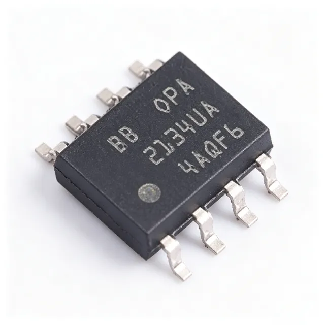
OPA2134UA/2K5 - Dual Audio Op-Amp 0.00008% THD | TI
OPA2134UA/2K5

OPA2134UA/2K5 - Dual Audio Op-Amp 0.00008% THD | TI

The Texas Instruments OPA2134UA/2K5 is a dual SoundPlus high-performance audio operational amplifier in an 8-pin SOIC package, supplied in 2,500-unit tape-and-reel format. It combines ultra-low distortion (0.00008% THD), low noise (8 nV/rtHz), true FET input (5 pA bias current), 20 V/us slew rate, and 8 MHz gain-bandwidth, operating from +/-2.5 V to +/-18 V supplies. An audio operational amplifier is a precision linear amplifier optimized to pass audio-band signals with minimal added harmonic distortion, noise, and phase error. It sits in the analog signal chain between transducers, DACs, and loudspeakers, and is a specialized subclass of the general op amp: an audio op amp is a linear amplifier within the analog signal processing chain of consumer, professional, and automotive audio electronics. Key features include the 0.00008% total harmonic distortion figure that keeps the device transparent in the audible signal path, 8 nV/rtHz voltage noise for low hiss in high-gain stages, and 5 pA FET input bias current that prevents loading of high-impedance sources such as guitar pickups and passive EQ networks. The 8 MHz bandwidth and 20 V/us slew rate preserve full-power performance across the entire 20 Hz to 20 kHz audio band, and the wide +/-18 V supply range matches standard professional audio rails. Architecturally, the OPA2134 uses a true FET input stage with a high open-loop gain of 600 V/mV (per TI datasheet), delivering excellent DC precision alongside audio-grade AC performance. The dual-channel SOIC-8 configuration enables compact stereo designs without performance compromise, and the single (OPA134) and quad (OPA4134) family members share identical core specifications for BOM flexibility. Typical applications include audio DAC output buffering (I/V conversion), line drivers, active crossovers, microphone preamplifiers, and audio test instrumentation, where the OPA2134UA/2K5 is often the limiting factor in signal purity. Design tip: bypass each supply pin with a 0.1 uF ceramic capacitor placed close to the package, and maintain adequate input/output headroom since this is not a rail-to-rail op amp. Prices as of 2026-08-30.

詢價 聯絡我們
OPA2134UA/2K5 - Dual Audio Op-Amp 0.00008% THD | TI
OPA2134UA/2K5

OPA2134UA/2K5 - Dual Audio Op-Amp 0.00008% THD | TI

The Texas Instruments OPA2134UA/2K5 is a dual SoundPlus high-performance audio operational amplifier delivering 0.00008% total harmonic distortion, 8 nV per root-hertz input voltage noise, and a 20 V/us slew rate in an 8-pin SOIC package, supplied in 2,500-unit tape-and-reel format. An audio operational amplifier is a precision linear amplifier optimized to pass audio-band signals with minimal added harmonic distortion, noise, and phase error. It sits in the analog signal chain between transducers, DACs, and loudspeakers, and is a specialized subclass of the general op amp: an audio op amp is a linear amplifier within the analog signal processing chain of consumer, professional, and automotive audio electronics. Key features include the 0.00008% total harmonic distortion figure that keeps the device transparent in the audible signal path, 8 nV/rtHz voltage noise for low hiss in high-gain stages, and 5 pA FET input bias current that prevents loading of high-impedance sources such as guitar pickups and passive EQ networks. The 8 MHz gain-bandwidth product and 20 V/us slew rate preserve full-power performance across the entire 20 Hz to 20 kHz audio band, and the wide +/-2.5 V to +/-18 V supply range matches standard professional audio rails. Architecturally, the OPA2134 uses a true FET input stage with a high open-loop gain of 600 V/mV per the TI datasheet, delivering excellent DC precision alongside audio-grade AC performance. The dual-channel SOIC-8 configuration enables compact stereo designs without performance compromise, and the single (OPA134) and quad (OPA4134) family members share identical core specifications for BOM flexibility. Typical applications include audio DAC output buffering (I/V conversion), line drivers, active crossovers, and microphone preamplifiers, where the OPA2134UA/2K5 is often the limiting factor in signal purity. Design tip: bypass each supply pin with a 0.1 uF ceramic capacitor placed close to the package, and maintain adequate input/output headroom since this is not a rail-to-rail op amp. This page synthesizes distributor pricing, drop-in alternatives, pinout data, and practical design notes not found in the manufacturer datasheet.

USD $0.92 聯絡我們