產品(39,000+)

XCKU3P-1FFVD900I - Kintex UltraScale+ FPGA | AMD
XCKU3P-1FFVD900I

XCKU3P-1FFVD900I - Kintex UltraScale+ FPGA | AMD

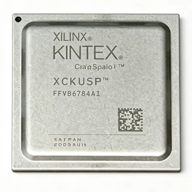
The AMD XCKU3P-1FFVD900I is a Kintex UltraScale+ field-programmable gate array with 355,950 logic cells, 20,340 configurable logic blocks, 304 input/outputs, and a nominal 0.85 V supply in a 900-BBGA FCBGA package. The -1 designation identifies the device speed grade, while the D900 package and industrial suffix distinguish its mechanical, thermal, and qualification configuration. A field-programmable gate array is a programmable digital integrated circuit whose configurable logic blocks, interconnects, memory resources, and input/output resources can be tailored after manufacture. The FPGA belongs to the Kintex UltraScale+ product family and sits within the broader semiconductor and programmable-logic hierarchy. This makes it suitable when a design needs substantial parallel processing capacity, flexible interfaces, and a hardware platform that can be revised through downloadable configuration data rather than redesigned as a fixed-function ASIC. The listed device provides 355,950 logic cells organized into 20,340 configurable logic blocks, with 304 input/outputs available for board-level connections. Its 31,641,600 memory bits support data storage and buffering within the programmable fabric. The 0.85 V nominal core voltage reflects the high-performance architecture of the Kintex UltraScale+ family, while the 900-BBGA FCBGA package provides a large pin and interconnect platform suitable for complex systems. The XCKU3P device family is intended for applications requiring high logic density and flexible hardware behavior. Relevant uses include data processing, control systems, communications infrastructure, industrial automation, test and measurement equipment, and embedded signal-processing platforms. Its large programmable fabric allows parallel data paths and multiple control functions to be consolidated without developing a custom silicon device. The principal design consideration is package-level complexity. A 900-BBGA FCBGA requires careful PCB layout, dense escape routing, controlled power delivery, and assembly processes capable of handling fine-pitch balls. Board designers should use the AMD package pinout files and the relevant device documentation to assign every ball, power plane, configuration signal, and high-speed connection correctly. This page combines the device identification, package information, programmable resource counts, sourcing details, family alternatives, and practical design guidance in one engineering-focused reference. It helps designers distinguish speed-grade, package, and suffix differences before committing to a board layout or production configuration.

詢價 聯絡我們
XCKU3P-1SFVB784E - 355950-Logic-Cell Kintex UltraScale+ FPGA | AMD
XCKU3P-1SFVB784E

XCKU3P-1SFVB784E - 355950-Logic-Cell Kintex UltraScale+ FPGA | AMD

The AMD XCKU3P-1SFVB784E is a Kintex UltraScale+ field-programmable gate array with 355,950 logic elements, 20,340 logic blocks, 31,641,600 RAM bits, and 304 user I/O pins in a 784-pin FCBGA package. It uses the -1 speed grade and an E temperature-grade designation, making it suited to demanding programmable-logic, signal-processing, control, and high-speed interface systems. A field-programmable gate array, or FPGA, is a semiconductor whose digital logic can be configured after manufacture. FPGA devices combine programmable logic blocks, block RAM, programmable input/output resources, clocking, and high-speed serial transceivers on one device. The Kintex UltraScale+ family occupies the performance tier between general-purpose UltraScale devices and larger Virtex devices, providing substantial logic and memory capacity for advanced embedded systems. The target device contains 20,340 logic blocks, equivalent to 355,950 logic elements, and 31,641,600 bits of block RAM. Its 304 user I/O positions support digital interfaces, while the UltraScale+ architecture is designed for demanding clock rates, high-speed connectivity, and parallel processing. The listed operating supply range is 0.825 V to 0.876 V for the relevant internal supply condition. The XCKU3P-1SFVB784E combines the -1 performance grade with a 784-pin FCBGA package offering high I/O and power connectivity. This package complexity supports advanced board-level designs but requires a land grid, multilayer PCB construction, careful power delivery, and assembly processes capable of handling a large fine-pitch BGA. A matching FPGA configuration, clocking, memory interface, and board design are essential to achieve predictable performance. Typical uses include high-throughput data acquisition, industrial image and signal processing, communications infrastructure, accelerator control, high-speed networking, radar or aerospace processing, and embedded systems requiring programmable logic. The large RAM and logic resources make the device particularly appropriate for parallel datapaths that cannot be implemented efficiently in a microcontroller or smaller FPGA. Design planning should begin with the UltraScale package pinout files and the AMD FPGA design toolchain. Confirm the required voltage rails, decoupling network, clocking topology, transceiver requirements, configuration method, thermal conditions, and board-layer constraints before schematic capture. Use simulation and timing analysis before programming hardware because high-speed interfaces can expose signal-integrity and clock-distribution issues that are difficult to correct after fabrication. This product page combines the exact device identity, resource counts, package information, sourcing guidance, application analysis, and design-oriented comparison points into one engineering reference for evaluating the XCKU3P-1SFVB784E.

詢價 聯絡我們
XCKU3P-1SFVB784I - 256-I/O Kintex UltraScale+ FPGA | AMD
XCKU3P-1SFVB784I

XCKU3P-1SFVB784I - 256-I/O Kintex UltraScale+ FPGA | AMD

AMD XCKU3P-1SFVB784I is a Kintex UltraScale+ field-programmable gate array with 256 I/O, a 784-ball FCBGA package, and an industrial-temperature ordering suffix. It belongs to AMD’s XCKU3P device family and provides programmable logic resources for demanding embedded, communications, industrial, and test systems. The component uses the same device and package identity as the listed XCKU3P-L1SFVB784I while differing in its ordering code. A field-programmable gate array, or FPGA, is a semiconductor whose digital logic, interfaces, and processing blocks are configured after manufacture. An FPGA sits above basic programmable logic and fixed-function microcontrollers in the hardware hierarchy: configuration software creates a dedicated digital circuit from the FPGA’s configurable logic blocks, block RAM, DSP resources, high-speed I/O, and clocking resources. This makes an FPGA suitable when deterministic parallel processing, flexible interfaces, or field-updatable logic are more important than the simplicity of a microcontroller. The XCKU3P family is positioned for high-end signal-processing and connectivity designs. AMD describes Kintex UltraScale+ devices around a balance of performance, power, memory-interface capability, high-speed connectivity, and cost efficiency. The catalog listing for XCKU3P-1SFVB784I identifies 256 I/O and the 784-BFBGA FCBGA package. Exact logic-cell, memory, transceiver, speed-grade, and electrical details must be confirmed against the device-specific AMD documentation before final design release. The “1” ordering suffix identifies the performance class used for this ordering code, while “SFVB784” identifies the package configuration. The final “I” denotes the industrial-temperature ordering option. Package construction is important for this device because a 784-ball FCBGA requires controlled board assembly, a multilayer PCB, appropriate via and escape routing, and careful power-delivery design to support the FPGA’s high pin count and performance requirements. Typical uses include industrial control and automation, high-speed data acquisition, communications infrastructure, instrumentation, embedded processing, and prototyping systems requiring programmable logic. The 256-I/O interface supports external memory, transceivers, clocks, and application-specific peripherals when the selected device resources and speed grades support those interfaces. Designers should preserve the exact SFVB784 footprint, verify every power rail and decoupling requirement in the AMD pinout and package documentation, and confirm that the selected configuration scheme matches the board’s boot architecture. Device migration also requires checking logical-cell usage, RAM, DSP, transceiver resources, pin constraints, timing closure, and the exact I/O standard rather than relying only on package similarity. This product record combines the exact XCKU3P-1SFVB784I catalog identity, package and I/O information, available manufacturer resources, same-family drop-in candidates, and practical implementation guidance. It is intended to accelerate engineering evaluation while keeping footprint, configuration, thermal, and signal-integrity verification tied to the official AMD documentation.

詢價 聯絡我們
XCKU3P-2FFVA676E Kintex UltraScale+ FPGA | AMD
XCKU3P-2FFVA676E

XCKU3P-2FFVA676E Kintex UltraScale+ FPGA | AMD

AMD XCKU3P-2FFVA676E is a Kintex UltraScale+ field-programmable gate array with 355,950 logic cells, 20,340 configurable logic blocks, and 304 input/output connections in a 676-BBGA FCBGA package. Its nominal core voltage is 0.85 V, making it a high-density programmable-logic device for demanding embedded, digital signal processing, networking, storage, and signal-processing systems. A field-programmable gate array, or FPGA, is a semiconductor whose digital logic is configured after manufacture. Within the broader hierarchy, an FPGA is a programmable-logic IC and a member of the semiconductor family. Unlike a fixed-function application-specific integrated circuit, an FPGA can combine parallel processing, serial connectivity, memory interfaces, and dedicated hardware blocks in one device. The Kintex UltraScale+ family targets designs that require substantially more programmable logic than midrange devices while retaining high-speed serial capabilities. The XCKU3P-2FFVA676E combines 355,950 logic cells with 20,340 configurable logic blocks and 304 I/O locations. Its FCBGA package supports dense board-level integration and is appropriate for sophisticated systems in which pin count, routing capacity, and processing throughput are central design constraints. The -2 ordering designation identifies the device speed option, while the FFVA676E suffix identifies the package and ordering characteristics. Detailed electrical limits, memory organization, and transceiver ratings must be confirmed in the AMD datasheet before schematic release. Programmable resources make the device suitable for parallel datapaths, protocol bridging, real-time filtering, control processing, and hardware-assisted acceleration. The 304 I/O connections provide substantial board-level connectivity for control signals, memory interfaces, clocks, data buses, and high-speed links. Designers should allocate pins according to the UltraScale package pinout files and account for bank-specific supply requirements, reference routing, and high-speed layout constraints. Typical uses include network-interface equipment, industrial imaging and control, test-and-measurement systems, storage controllers, communications infrastructure, and embedded signal-processing platforms. In each case, the FPGA can implement multiple time-critical functions in parallel, reducing reliance on separate programmable controllers or discrete logic devices. The primary design consideration is package-level complexity. A 676-ball FCBGA demands careful escape routing, dense via structures, controlled impedance, clean power delivery, and assembly process capability. Use the AMD package pinout files and board-design guidance to validate every ball assignment, voltage rail, decoupling network, and high-speed interface before fabrication. This product page consolidates the verified device identity, package, programmable-resource figures, compatible same-family ordering options, and practical implementation guidance. It helps engineers compare alternatives and plan a PCB without obscuring the essential distinction between a true pin-compatible option and a broader Kintex UltraScale+ equivalent.

詢價 聯絡我們
XCKU3P-2FFVA676I - Kintex UltraScale+ FPGA | AMD BGA
XCKU3P-2FFVA676I

XCKU3P-2FFVA676I - Kintex UltraScale+ FPGA | AMD BGA

The AMD XCKU3P-2FFVA676I is a Kintex UltraScale+ field-programmable gate array in a 676-ball BGA package, designed for systems requiring programmable logic, high-speed digital processing, and flexible hardware acceleration. The device contains 355,950 programmable logic cells and is identified as an industrial-grade FPGA with a -2 speed designation. Its 676-BBGA, FCBGA construction supports dense board-level integration without exposing fine-pitch leads. A field-programmable gate array is a semiconductor whose digital logic, interfaces, and processing blocks are configured after fabrication. The FPGA product hierarchy extends from programmable logic devices to FPGAs, programmable-logic ICs, and semiconductor devices. Within the Kintex UltraScale+ family, this device provides a high-capacity implementation platform for communications, industrial control, data processing, networking, and embedded systems where hardware parallelism can improve throughput and reduce external component count. The 355,950-cell configuration offers substantial logic capacity for designs that combine control logic, data pipelines, serial interfaces, and dedicated accelerator functions. The -2 ordering code denotes the device's speed grade, while the final I character identifies the industrial temperature option. Its BGA package provides a large number of electrical contacts compared with leaded packages, enabling extensive power, ground, configuration, and general-purpose I/O connections within a compact board footprint. Programmable-logic designs are typically created with FPGA development tools, compiled into a configuration bitstream, and loaded into the device through a supported configuration interface. The implementation must account for the BGA's dense ball pitch, power-grid connectivity, decoupling requirements, and high-speed routing constraints. Because configuration and I/O standards are system-dependent, board designers should use the AMD package pinout files and device documentation when assigning every ball and defining power planes. Typical uses include high-throughput signal processing, industrial automation, network-interface functions, test equipment, embedded control, and accelerator modules. The device is especially appropriate when parallel hardware architecture can outperform a sequential processor for repetitive filtering, protocol handling, or data movement. The -2 speed grade and industrial temperature marking make the part relevant to equipment expected to operate across extended industrial temperature conditions. A critical design consideration is that the 676-ball BGA cannot be treated as a simple two-row IC footprint. Follow the AMD package pinout files, provide continuous decoupling near the device, maintain the required power and ground ball assignments, and validate escape routing before fabrication. Signal-integrity and thermal performance depend on the completed stack-up, layer count, return paths, and power-delivery network rather than on the IC alone. This product page organizes the key electrical identity, package details, application guidance, design constraints, comparison information, and same-family migration options into a practical engineering reference. Use the manufacturer documentation for the authoritative pin assignment, complete electrical limits, configuration procedure, and design-support files before releasing a PCB or production design.

詢價 聯絡我們
XCKU3P-2FFVB676E - Kintex UltraScale+ FPGA | AMD
XCKU3P-2FFVB676E

XCKU3P-2FFVB676E - Kintex UltraScale+ FPGA | AMD

AMD XCKU3P-2FFVB676E is a Kintex UltraScale+ field-programmable gate array (FPGA) supplied in a 676-ball FCBGA package. The catalog listing identifies the device as a programmable-logic IC with 280 I/O positions, making it suitable for systems that require substantial parallel connectivity, configurable processing blocks, and programmable digital logic. The “XCKU3P” ordering code places it in AMD’s Kintex UltraScale+ FPGA product family, while “-2” identifies the performance grade used in the part designation. An FPGA is a semiconductor whose digital behavior is configured after manufacture. The FPGA hierarchy begins with the individual configurable logic block, expands into an FPGA device, and ultimately belongs to the broader semiconductor and programmable-logic categories. This lets engineers implement parallel datapaths, protocol controllers, signal processing, control logic, and hardware accelerators without relying exclusively on a fixed-function processor. Configurable routing resources connect the selected logic, memory, input/output, clocking, and dedicated hard blocks. The principal catalog-level benefits of XCKU3P-2FFVB676E are its Kintex UltraScale+ family assignment, 280 I/O positions, -2 performance grade, and 676-ball FCBGA construction. The high pin count supports dense board-level integration and broad external connectivity, while the FPGA architecture permits a single physical device to consolidate functions that might otherwise require several programmable or fixed-function components. The exact logic-cell, DSP, memory, transceiver, power, and temperature limits should be confirmed in the applicable AMD family documentation for the selected device and package. The “P” designation in the ordering code should not be interpreted without the AMD ordering guide because its exact commercial meaning depends on the family documentation. Likewise, the “2” speed grade is a family-level ordering designation, not by itself a complete description of operating frequency or performance. Engineers should use the package pinout files, device datasheet, configuration guidance, and power-estimation workflow when preparing a board or selecting a replacement. Typical applications for this device include high-speed data acquisition, industrial control and automation, communications infrastructure, signal-processing systems, test and measurement equipment, and embedded accelerator platforms. In each case, the FPGA is configured to implement the required datapath and control functions, while the 280 I/O positions provide connections to external converters, memories, interfaces, clocks, and control signals. A critical design consideration is that the 676-ball FCBGA footprint requires a dense multilayer PCB with a carefully engineered power-delivery network, decoupling strategy, ball-assignment review, and thermal assessment. Before layout, verify every supply, ground, configuration, clock, and user I/O connection against the current AMD package pinout file rather than inferring connectivity from the commercial ordering code. This product page combines the exact catalog identity, package information, price-evidence rules, replacement analysis, and practical design guidance. It is intended to help engineers identify the correct AMD device, locate authoritative documentation, assess genuine drop-in options, and move from component selection into PCB implementation with fewer specification and compatibility risks.

詢價 聯絡我們
XCKU3P-2FFVB676I - Kintex UltraScale+ FPGA | AMD
XCKU3P-2FFVB676I

XCKU3P-2FFVB676I - Kintex UltraScale+ FPGA | AMD

The AMD XCKU3P-2FFVB676I is a Kintex UltraScale+ field-programmable gate array in an FCBGA-676 package, combining 280 I/O with a -2 speed grade for performance-oriented programmable-logic designs. The device belongs to the Kintex UltraScale+ FPGA family and provides 162,720 configurable logic blocks in the device architecture, as reflected in the product listing data. A field-programmable gate array, or FPGA, is a semiconductor whose digital logic, memory, signal processing, and I/O behavior can be configured after manufacture. FPGAs occupy the programmable-logic portion of the semiconductor hierarchy, combining large parallel processing resources with programmable interconnect. This makes them useful for demanding digital systems that benefit from hardware parallelism, deterministic interfaces, and field-updatable functionality. The most prominent catalog characteristics are the 280 I/O, the -2 performance grade, and the FCBGA-676 package. The Kintex UltraScale+ designation identifies a high-end AMD/Xilinx FPGA platform, while the KU3P device designation distinguishes the specific configuration within that platform. The -2 suffix selects a particular speed grade, allowing designers to match device timing expectations to a particular system-performance target. The FCBGA-676 package provides a dense, board-level mounting solution with hundreds of connection points. Because such packages contain many power, ground, signal, configuration, and differential I/O balls, the PCB must use a qualified footprint, controlled escape routing, and careful power-plane distribution. AMD also publishes UltraScale package pinout files in TXT and CSV formats, with the file format described in UG575. Typical applications include high-speed signal processing, industrial control, communications infrastructure, test and measurement, embedded vision, and acceleration functions requiring substantial parallel programmable logic. The large I/O count supports systems that need numerous parallel connections, while the Kintex UltraScale+ resource level is suited to consolidated control and datapath designs rather than simple low-complexity programmable logic. A key design consideration is that this is a high-pin-count BGA device requiring careful escape routing, layer planning, decoupling, and thermal management. Do not assign package balls solely from a catalog page; use the AMD UltraScale package pinout files and the device-specific documentation for every power, ground, configuration, and I/O connection before release. This page organizes the exact order code, package information, verified specifications, purchase and lead-time guidance, package-related constraints, and engineering selection considerations. It also distinguishes catalog-confirmed attributes from detailed electrical, timing, and pin-level information that must be established from the appropriate AMD documentation and the final system design.

詢價 聯絡我們
XCKU3P-2FFVD900E - Kintex UltraScale+ FPGA | AMD
XCKU3P-2FFVD900E

XCKU3P-2FFVD900E - Kintex UltraScale+ FPGA | AMD

The AMD XCKU3P-2FFVD900E is a Kintex UltraScale+ field-programmable gate array built on a FinFET process, with 355,950 logic elements, 20,340 logic blocks, and 31,641,600 bits of block RAM. The device provides 304 user I/O and uses a 900-ball FCBGA package measuring 31 mm by 31 mm. Its specified core supply voltage is 0.825 V to 0.876 V. A field-programmable gate array, or FPGA, is a programmable digital semiconductor categorized within integrated circuits, semiconductors, and digital logic. Unlike a fixed-function application-specific integrated circuit, an FPGA combines programmable logic, block RAM, programmable I/O, and dedicated interface resources on one device. This architecture allows engineers to implement parallel processing, control, networking, signal processing, and hardware acceleration while retaining the flexibility to update designs after manufacture. The Kintex UltraScale+ family combines programmable logic with high-speed connectivity resources. The XCKU3P-2FFVD900E offers 355,950 logic elements organized into 20,340 LAB/CLB blocks and 31,641,600 RAM bits for on-chip storage. Its 304 user I/O support high pin density for parallel interfaces and board-level connectivity. AMD identifies the -2 part as the middle performance option within the device-speed and temperature-grade system. The 900-FCBGA package provides dense access to logic and I/O resources but requires a carefully designed PCB. Power delivery, ground-plane continuity, decoupling, and high-speed signal routing are central implementation concerns because the package exposes hundreds of balls in a 31 mm by 31 mm area. Designers should use the manufacturer pinout files and device documentation when assigning every power, ground, configuration, clock, and user-I/O connection. Typical applications include high-throughput signal processing, network packet handling, industrial control, test and measurement, video infrastructure, and embedded edge processing. The 304 user I/O are useful for parallel data acquisition and external memory connectivity, while the large block-RAM capacity supports buffering, lookup tables, and local data storage. The device is especially relevant when deterministic parallel hardware is more valuable than software-only flexibility. For a new PCB, use the AMD package pinout files, recommended power architecture, and PCB-design guidance before committing the 900-ball land pattern. Confirm the selected board file, power rails, decoupling network, configuration interface, and thermal strategy against the exact -2FFVD900E device. Firmware, bitstream, and board-level constraints must also be checked before hardware production. This product summary combines the device's published logic, memory, I/O, package, and supply information with practical implementation guidance. It also distinguishes the verified same-package speed-grade alternative and highlights where a new design should use the manufacturer pinout and power-design files rather than relying on generic BGA conventions.

詢價 聯絡我們
XCKU3P-2FFVD900I - 355,950 LEs Kintex UltraScale+ FPGA | AMD
XCKU3P-2FFVD900I

XCKU3P-2FFVD900I - 355,950 LEs Kintex UltraScale+ FPGA | AMD

AMD XCKU3P-2FFVD900I is a Kintex UltraScale+ field-programmable gate array with 355,950 logic cells, 12,960 Kb of block RAM, and 1,368 DSP slices in a 900-FCBGA package measuring 31 x 31 mm. The device uses the -2 speed grade and is specified for an industrial junction-temperature range of -40°C to 100°C. A field-programmable gate array, or FPGA, is a programmable semiconductor in which digital logic, interfaces, and parallel processing functions are configured through programmable bitstreams. FPGAs occupy the semiconductor hierarchy above fixed-function logic devices and provide hardware parallelism, reconfigurability, and deterministic real-time operation. The Kintex UltraScale+ family combines FPGA fabric with programmable logic, embedded memory, DSP resources, and high-speed serial connectivity for demanding signal-processing and data-center systems. The XCKU3P device provides 355,950 logic cells for implementing control logic, protocol bridges, packet processors, and parallel algorithms. Its 12,960 Kb of block RAM supports buffering, lookup tables, packet storage, and data-plane scratchpad requirements. The 1,368 DSP slices accelerate fixed-point and floating-point operations associated with filtering, modulation, error correction, and other digital signal-processing workloads. The listing identifies 304 I/O, while the FFVD900 package supports a high-density board layout that requires careful power, thermal, and signal-integrity engineering. The -2 designation identifies the device speed grade, allowing engineers to plan for the timing performance associated with this device within complete FPGA designs. The industrial temperature indication makes the part appropriate for equipment expected to operate across extended industrial temperature conditions, subject to the complete AMD device specifications and board-level thermal design. This device is programmed through the AMD adaptive-computing toolchain and requires a compatible FPGA configuration architecture, clocking, memory interface, and power-delivery system. Typical applications include high-throughput data processing, network packet handling, accelerator control, high-performance signal processing, video infrastructure, and communications equipment. The large logic and DSP resources allow multiple parallel pipelines to operate simultaneously, while block RAM reduces reliance on external memory for short-latency buffering. System clocking and power sequencing remain central because performance depends on the complete board and design implementation rather than on logic-cell counts alone. For a new design, place all power and ground connections directly under their assigned BGA balls, preserve the AMD reference-design layer stack, and keep high-speed routing short. Check junction temperature under the worst-case activity and ambient conditions, provide suitable power-decoupling networks, and validate signal integrity with the package and board models published for the FFVD900 device. Confirm bitstream compatibility and pin assignments in the current package files before releasing PCB artwork. This page combines the verified device specifications, source references, replacement analysis, comparison data, and practical integration guidance needed to evaluate the XCKU3P-2FFVD900I for industrial FPGA and adaptive-computing systems.

詢價 聯絡我們
XCKU3P-2SFVB784E - Kintex UltraScale+ 304 I/O 784-BFBGA FPGA
XCKU3P-2SFVB784E

XCKU3P-2SFVB784E - Kintex UltraScale+ 304 I/O 784-BFBGA FPGA

The AMD XCKU3P-2SFVB784E is a Kintex UltraScale+ field-programmable gate array in a 784-BFBGA FCBGA package. It provides 304 I/O, approximately 31,641,600 logic cells, and approximately 355,950 LUTs. The -2 speed designation identifies the performance grade used in the AMD Xilinx ordering code, while the SFVB784E portion identifies the device and package configuration. A field-programmable gate array is a programmable digital integrated circuit. An FPGA belongs to the semiconductor and programmable-logic hierarchy, combining configurable logic blocks, programmable I/O, embedded memory, dedicated arithmetic resources, and clocking and routing resources. Unlike a fixed-function application-specific integrated circuit, an FPGA can be reprogrammed for different algorithms, interfaces, and system architectures after manufacture. The Kintex UltraScale+ family is designed for high-performance programmable systems. In this part, the combination of 304 I/O and a large logic-resource count supports designs requiring substantial parallel processing, broad external connectivity, and high-speed data movement. The 784-BFBGA package provides a dense surface-mount implementation for complex systems rather than a simple discrete-package design. The 784-BFBGA format is intended for high-density PCB layouts. Its ball grid requires careful escape-routing, power-plane distribution, thermal management, and BGA assembly process control. Because the package contains a large programmable device, designers should plan decoupling, regulated supplies, clocking, configuration memory, and download or boot interfaces before finalizing the PCB. Typical uses include high-speed data acquisition, test and measurement, communications infrastructure, industrial control, video processing, and accelerator or prototyping systems. The FPGA's parallel architecture can accelerate workloads that benefit from configurable pipelines, parallel lanes, and hardware-constrained data paths. The exact performance of any such system depends on the selected clocking resources, memory interface implementation, I/O standards, and device configuration. For PCB implementation, use the AMD package pinout and mechanical files for the exact ordering code. Check all power, ground, configuration, clock, and I/O assignments against the manufacturer package documentation before fabrication. Treat the 784-BFBGA footprint as a high-density assembly design rather than a conventional two-row leaded package. This product page organizes the core device identity, package information, application guidance, replacement analysis, and engineering-oriented selection notes for engineers evaluating the XCKU3P-2SFVB784E.

詢價 聯絡我們
XCKU3P-2SFVB784I - 304 I/O Kintex UltraScale+ FPGA | AMD
XCKU3P-2SFVB784I

XCKU3P-2SFVB784I - 304 I/O Kintex UltraScale+ FPGA | AMD

The AMD Xilinx XCKU3P-2SFVB784I is a Kintex UltraScale+ field-programmable gate array with 304 I/O, housed in a 784-FCBGA surface-mount package. The device is identified by the XCKU3P family designation, a -2 speed-grade suffix, the SFVB784 package code, and an industrial-temperature suffix I. Its core supply specification is 0.825 V to 0.876 V, and its operating junction-temperature specification is -40°C to 100°C. The device is intended for designs requiring parallel programmable logic, high-speed serial connectivity, embedded processing, and substantial general-purpose FPGA resources. A field-programmable gate array is a semiconductor whose digital functions are defined after manufacture by loading a configuration bitstream. FPGA devices occupy the practical space between fixed-function logic and application-specific integrated circuits. The Kintex UltraScale+ family uses programmable logic blocks, block RAM, DSP resources, high-speed transceivers, and dedicated input/output resources to implement parallel datapaths, control systems, protocol bridges, signal processing, and accelerator logic. The XCKU3P designation identifies a mid-density member of that architecture. The -2 suffix identifies the performance grade of this cataloged device. The SFVB784 designation identifies the 784-FCBGA package, which supports a high pin count for power delivery, configuration signals, user I/O, and high-speed interfaces. With 304 user I/O available, the device is particularly appropriate for systems that need substantial board-level connectivity rather than only a small control interface. Package assignment remains critical: the device must be treated as a complex BGA assembly requiring controlled assembly, inspection, and thermal design. The XCKU3P-2SFVB784I is suitable for industrial communications equipment, test and measurement systems, industrial automation, high-speed data acquisition, signal processing, embedded control, and network infrastructure. Its programmable architecture allows field updates and product differentiation without changing the PCB layout. Designers should balance logic utilization, transceiver requirements, power budgeting, pin assignment, and the thermal constraints of a large BGA package before finalizing the implementation. One important design consideration is that the specified 0.825 V to 0.876 V range is a core supply requirement rather than a complete power-supply specification. A complete board design must follow the AMD power, decoupling, configuration, and package guidelines for this device family. The operating junction-temperature range also requires thermal analysis that includes ambient conditions, board copper, heat sinks, airflow, and power dissipation from the configured design. This product record combines the exact catalog identity, package details, electrical limits, pinout-resource location, sourcing context, and engineering guidance into one reference. It also distinguishes genuine same-footprint alternatives from parts that may use a different package or device architecture, helping designers avoid an apparently similar MPN that cannot replace the target on an existing PCB.

詢價 聯絡我們
XCKU5P-1FFVA676E - 256 I/O Kintex UltraScale+ | AMD
XCKU5P-1FFVA676E

XCKU5P-1FFVA676E - 256 I/O Kintex UltraScale+ | AMD

AMD XCKU5P-1FFVA676E is a Kintex UltraScale+ field-programmable gate array with 256 I/O, 41,984,000 catalog logic cells, 474,600 catalog logic registers, and a 676-ball FCBGA package. The -1 speed designation identifies the device performance grade, while the FFVA676E ordering code identifies the Kintex UltraScale+ family, package construction, and ordering configuration used by this part. A field-programmable gate array, or FPGA, is a reconfigurable semiconductor in which digital logic, block memory, signal processing, and programmable I/O are organized into programmable architecture. Within the semiconductor hierarchy, an FPGA belongs to the programmable-logic device class and combines parallel programmable logic fabric with configurable peripherals. This makes the XCKU5P family suitable when design flexibility, parallel processing, high-speed interfaces, and deterministic hardware operation must coexist in one device. The XCKU5P-1FFVA676E provides 256 I/O in a 676-FCBGA package, giving a board designer access to a substantial pin count for external memory, high-speed serial links, clocks, data acquisition, control interfaces, and general-purpose digital logic. Its catalog figures of 41,984,000 logic cells and 474,600 logic registers describe the density of its programmable architecture, while the Kintex UltraScale+ platform provides resources for demanding parallel-processing and signal-processing designs. The FFVA676E device is associated with the AMD Kintex UltraScale+ product generation and supports an integrated combination of programmable logic and dedicated hardware resources. Designers can allocate logic for control paths, implement parallel algorithms in fabric, use dedicated resources for DSP-style arithmetic, and map high-speed interfaces according to the device architecture. Exact clock, transceiver, memory, power, and I/O standards should be confirmed against the current AMD data sheet before schematic signoff. Typical applications include high-throughput signal processing, industrial imaging, radar and communications infrastructure, test and measurement systems, data acquisition, network acceleration, and embedded control with substantial parallel logic. The 256-I/O count is particularly useful when a design needs substantial board-level connectivity while retaining a single-programmable-device implementation rather than combining an FPGA with multiple support devices. Board planning should prioritize the AMD UltraScale package pinout files, power-decoupling strategy, thermal management, and high-speed layout rules. A 676-FCBGA device normally requires multilayer PCB construction, controlled escape routing, and careful treatment of supply and ground planes. Use the package pinout files and the AMD device documentation when assigning balls, planning power rails, and validating every board-level connection. This product summary combines the exact catalog attributes for the XCKU5P-1FFVA676E with application guidance, package considerations, and clearly defined alternatives. It is intended to accelerate component identification and initial design planning while directing final electrical, thermal, timing, and compliance decisions to the current AMD documentation.

詢價 聯絡我們
XCKU5P-1FFVB676E - 280-I/O Kintex UltraScale+ FPGA | AMD
XCKU5P-1FFVB676E

XCKU5P-1FFVB676E - 280-I/O Kintex UltraScale+ FPGA | AMD

The AMD Xilinx XCKU5P-1FFVB676E is a Kintex UltraScale+ field-programmable gate array built on FinFET process technology, with 474,600 logic cells, 280 I/O, 17,280 Kb of block RAM, and 1,824 DSP slices in a 676-pin FCBGA package measuring 27 x 27 mm. The -1 suffix identifies its speed grade, while the E suffix identifies the extended-temperature option. Its operating range is specified from 0°C to 100°C at the junction. A Kintex UltraScale+ FPGA is a programmable semiconductor used to implement digital control, data processing, signal processing, networking, and embedded systems. Within the FPGA hierarchy, it combines configurable logic blocks, block RAM, DSP resources, programmable I/O, dedicated clocking, and high-speed serial transceivers. This balance makes the device useful when designers need substantial parallel processing resources while retaining the flexibility of reconfigurable hardware. The XCKU5P-1FFVB676E provides 474,600 logic cells for control logic and complex digital pipelines, together with 1,824 DSP slices for filtering, modulation, correlation, fixed-point arithmetic, and other multiply-accumulate-intensive tasks. Its 17,280 Kb of block RAM provides on-chip storage for packet buffers, waveform data, lookup tables, and data-plane staging. The 280 I/O expand board connectivity without relying primarily on external serial links. The Kintex UltraScale+ architecture uses a FinFET implementation to combine high logic density with performance and power efficiency. Its device-specific configuration, bitstream, package pinout, and power characteristics must be handled as one design target rather than as interchangeable generic FPGA parameters. UltraScale+ package pinout resources and AMD product documentation should be used to verify each ball assignment, differential-pair polarity, supply requirement, and configuration connection before schematic or PCB signoff. Typical uses include industrial machine vision, high-throughput data acquisition, digital communications, radar and signal-processing front ends, network infrastructure, test equipment, and high-speed protocol bridges. The combination of DSP slices and block RAM makes the device suitable when algorithm behavior or system requirements may evolve faster than a fixed ASIC design cycle. Its 280 I/O also supports parallel sensors, converters, memory interfaces, and board-level control signals. Design planning should account for the 676-ball FCBGA footprint, multilayer PCB construction, controlled-impedance routing, separate power distribution, decoupling, thermal management, and configuration-signal handling. Differential and high-speed interfaces require trace-length matching and reference-plane continuity, while the 27 x 27 mm package demands careful escape routing from its dense ball array. Prototype platforms can reduce hardware risk before a production board is committed. This page combines the verified device identity, package and resource details with practical application guidance, same-package migration options, and engineering-focused design notes. The comparisons emphasize how speed grade, temperature grade, resource capacity, package, and qualification requirements affect replacement decisions rather than treating every Kintex UltraScale+ FPGA as interchangeable.

詢價 聯絡我們
XCKU5P-1FFVD900E - 304-I/O Kintex UltraScale+ FPGA | AMD
XCKU5P-1FFVD900E

XCKU5P-1FFVD900E - 304-I/O Kintex UltraScale+ FPGA | AMD

The AMD XCKU5P-1FFVD900E is a Kintex UltraScale+ field-programmable gate array with 304 I/O, a 900-BBGA FCBGA package, and a -1 speed grade. It is designed for high-performance programmable logic in systems requiring extensive parallel connectivity, substantial on-chip FPGA resources, and deterministic control over digital data paths. AMD identifies the device as an FPGA rather than a fixed-function processor, allowing designers to implement application-specific logic, interfaces, and signal processing directly in programmable hardware. A field-programmable gate array is a semiconductor device whose digital circuits are configured after manufacture. In the product hierarchy, an FPGA is an integrated circuit containing programmable logic blocks, programmable I/O, memory resources, clocking, and dedicated signal-processing or serial connectivity blocks. Unlike application-specific integrated circuits, an FPGA allows architecture, interfaces, and logic behavior to be revised through bitstream updates, making it useful where requirements evolve or product variants share common hardware. The XCKU5P-1FFVD900E provides 304 I/O in a 900-BBGA FCBGA package. Its high I/O count supports dense board-level interconnections between the FPGA, external memory, network transceivers, data converters, and high-speed peripherals. The -1 designation identifies the selected performance grade for design planning. Exact core count, embedded-memory capacity, transceiver count, speed grades, and operating-temperature limits must be confirmed against the AMD device table and package documentation before a design is released. The device belongs to the Kintex UltraScale+ generation, which combines programmable logic with high-speed serial connectivity and substantial digital processing resources. The package's 900-ball arrangement creates a compact land pattern but also requires a dense PCB escape strategy. Ball assignment, power rails, decoupling requirements, and high-speed routing rules should be taken directly from AMD's package pinout files and the applicable UltraScale design guidance rather than inferred from a generic BGA footprint. Typical uses include high-speed data acquisition, test and measurement, industrial control, communications infrastructure, signal processing, accelerator prototyping, and secure control systems. The 304-I/O interface is especially useful when a design must connect multiple converters, memory devices, clock sources, and fabric resources without using a larger board package. For a specific product qualification, engineers should verify transceiver line rates, supported protocols, memory interfaces, and power budgets against the intended architecture. A successful implementation requires careful power planning, multilayer PCB construction, and controlled clocking. The 900-BBGA package demands short, low-inductance connections from power supplies to the appropriate balls and short return paths for high-speed signals. Decoupling, simulation, thermal analysis, and Bitstream-generation tool versions should be validated early because package assignment and device-support differences can affect implementation results. This product summary combines the exact AMD orderable MPN, package identity, I/O count, and available documentation entry points with practical guidance for FPGA selection, PCB implementation, and qualification. It also distinguishes verified orderable information from device details that require confirmation in AMD's current Kintex UltraScale+ selection and package documentation.

詢價 聯絡我們
XCKU5P-1FFVD900I - Kintex UltraScale+ FPGA | AMD
XCKU5P-1FFVD900I

XCKU5P-1FFVD900I - Kintex UltraScale+ FPGA | AMD

AMD XCKU5P-1FFVD900I is a Kintex UltraScale+ field-programmable gate array built on 20 nm technology, with 474,600 logic cells, 27,120 configurable logic blocks, and a 900-ball FCBGA package. The device operates at a stated 0.72 V core voltage and is intended for industrial-temperature applications operating from -40°C to +100°C. A field-programmable gate array is a reconfigurable digital semiconductor in which programmable logic blocks, programmable input/output resources, embedded memory, clocking, and dedicated serial transceivers form a flexible hardware platform. Kintex UltraScale+ devices belong to the FPGA hierarchy and combine parallel programmable logic with high-speed serial connectivity, supporting designs that benefit from hardware parallelism, rapid prototyping, and field-updatable configurations. Principal characteristics include 474,600 logic cells and 27,120 configurable logic blocks in a -1 performance grade. The 900-ball FCBGA package supports dense, high-performance interconnect requirements, while the industrial temperature designation supports operation from -40°C to +100°C. The device combines large programmable logic capacity with integrated high-speed resources for demanding communications, processing, storage, and test systems. The -1 suffix identifies the device performance grade within AMD's Kintex UltraScale+ ordering scheme. Device configuration is handled through the AMD FPGA programming ecosystem, and board-level implementation must follow the package pinout, power architecture, decoupling, clocking, and thermal guidelines in the Kintex UltraScale+ documentation. Exact I/O counts, memory totals, transceiver ratings, power limits, and configuration interface details require the corresponding manufacturer tables for the selected device. Typical implementation areas include high-speed data conversion, industrial networking, test and measurement, video and image processing, communications infrastructure, and compute-intensive accelerator prototypes. The large logic-cell count supports parallel datapaths, while integrated serial interfaces can reduce external component count in systems requiring high-bandwidth links. A successful design depends on PCB escape routing from the 900-ball package, adequate multi-rail supply sequencing, thermal management, and signal-integrity control on high-speed interfaces. Use the AMD package files and design tools to validate pin assignments and timing rather than relying on generic BGA layouts, because ball location, power planes, and high-speed routing determine whether the selected FPGA achieves its intended performance. This page combines the exact device identity, package and capacity characteristics with practical FPGA design guidance, available sourcing data, comparison parameters, and same-family replacement considerations. It also distinguishes true same-footprint choices from broader FPGA alternatives that may require a different package, power design, or device migration.

詢價 聯絡我們
XCKU5P-1SFVB784E - 304 I/O Kintex UltraScale+ FPGA | AMD
XCKU5P-1SFVB784E

XCKU5P-1SFVB784E - 304 I/O Kintex UltraScale+ FPGA | AMD

The AMD XCKU5P-1SFVB784E is a Kintex UltraScale+ field-programmable gate array in a 784-ball FCBGA package, providing 304 user I/O and approximately 216,960 configurable logic blocks. The -1 suffix identifies the device speed grade, while SFVB784E denotes the specific package, temperature, and ordering configuration. This combination of high logic capacity and a large I/O count makes the FPGA suitable for systems requiring parallel interfaces, substantial parallel processing, programmable control, or hardware acceleration. A field-programmable gate array is a semiconductor whose digital functions are defined after fabrication by loading a configuration bitstream. An FPGA belongs to the broader programmable-logic hierarchy alongside complex programmable logic devices, while its internal architecture commonly includes programmable logic, block RAM, DSP resources, high-speed I/O, clocking, and configuration interfaces. Kintex UltraScale+ devices balance general-purpose programmable logic with dedicated resources for data processing and high-speed serial connectivity. The principal feature of the XCKU5P-1SFVB784E is its combination of approximately 216,960 logic blocks and 304 I/O in one 784-ball FCBGA package. Its -1 speed grade provides a distinct operating-performance class within the Kintex UltraScale+ family. The device listing also identifies 304 I/O, making the package especially relevant to designs that cannot be implemented with a smaller or lower-pin-count FPGA. Exact internal RAM, DSP, transceiver, voltage, and performance figures require confirmation in the AMD device documentation before final design release. For power, clocking, and board planning, the 784-ball package demands careful assignment of power rails and controlled layout around high-speed interfaces. Although the device combines extensive programmable resources, utilization depends on the architecture selected in the AMD Vivado design environment and on the speed, memory, and I/O requirements of the final bitstream. Design reviews should compare the actual resource totals reported by the tool against the device limits. Typical uses include high-speed data acquisition, network interface control, industrial automation, test equipment, signal processing, protocol bridging, and embedded accelerator systems. The large I/O count can simplify designs that otherwise require several programmable devices, while the high logic-block count supports parallel datapaths and complex control logic. Any replacement assessment must preserve the exact FCBGA footprint, power architecture, configuration behavior, speed grade, and device identifiers. A critical design consideration is that equivalent-looking FPGA order codes are not automatically interchangeable. Pin compatibility depends on the exact package drawing, while functional compatibility depends on voltage rails, configuration pins, exposed resources, and the selected bitstream target. Review the AMD package pinout and device tables before substituting any part, and reserve at least one complete hardware validation cycle for any proposed alternate device. This page consolidates the available device identity, package, I/O, and logic-block information with practical FPGA design guidance, sourcing paths, and structured engineering comparisons. It is intended to accelerate initial component selection while keeping final resource, power, timing, and pin-level decisions tied to AMD's authoritative documentation.

詢價 聯絡我們
XCKU5P-1SFVB784I - 474,600-Cell Kintex UltraScale+ FPGA | AMD
XCKU5P-1SFVB784I

XCKU5P-1SFVB784I - 474,600-Cell Kintex UltraScale+ FPGA | AMD

The AMD XCKU5P-1SFVB784I is a Kintex UltraScale+ field-programmable gate array with 474,600 logic cells, 27,120 LABs/CLBs, 41,984,000 RAM bits, and 304 user I/O in a 784-FCBGA package. It is the -1 speed grade, operates from a 0.825 V to 0.876 V supply, and supports a -40°C to 100°C junction-temperature range. A field-programmable gate array, or FPGA, is a programmable semiconductor in which the digital logic, interconnect, and many digital peripherals are configured after manufacture. Within the product hierarchy, the XCKU5P-1SFVB784I is a Kintex UltraScale+ FPGA, an FPGA and CPLD device, an integrated circuit, and ultimately a semiconductor. Its combination of logic resources, block RAM, programmable I/O, and a large BGA package supports parallel data processing, high-throughput interfaces, and embedded control functions. The device provides 304 user I/O, 474,600 logic cells, 27,120 LABs/CLBs, and 41,984,000 total RAM bits. These resources allow substantial parallel processing and data buffering within one programmable device. Its 784-FCBGA package provides the interconnect density required by this Kintex UltraScale+ configuration, while the listed 23 mm by 23 mm package dimensions support high-density board layouts that require careful escape-routing and thermal planning. The -1 designation identifies the device speed grade, making this MPN appropriate when the design requires the -1 operating class rather than a faster grade. A configurable supply range of 0.825 V to 0.876 V applies to the core-supply specification reported for this exact device. Engineers must use the UltraScale package pinout files and device documentation when assigning power rails, configuring banks, and implementing the 784-position land pattern. Typical applications include industrial automation, high-speed data acquisition, signal processing, communications infrastructure, embedded vision, and accelerator-style parallel processing. The large logic and RAM resources are especially useful where multiple independent pipelines must operate concurrently, while the 304 user I/O can reduce the need for external interface logic when the board-level pin plan supports the device’s bank architecture. A critical design consideration is the 784-FCBGA footprint. High-density escape routing, via-in-pad requirements where specified, power-plane segmentation, decoupling, and the exposed thermal-management strategy must be designed together. Device configuration, bitstream generation, and pin constraints should be checked against the package-specific UltraScale documentation before schematic or PCB signoff. This product page organizes the exact device identity, core capacity, memory, I/O count, package details, pinout resources, and practical configuration considerations into one engineering reference. It also distinguishes true same-package replacement options from broader FPGA alternatives, helping design teams assess speed-grade, temperature-grade, and supply compatibility before committing a 784-FCBGA layout.

詢價 聯絡我們
XCKU5P-2FFVB676I - Kintex UltraScale+ FPGA 474K LC | AMD
XCKU5P-2FFVB676I

XCKU5P-2FFVB676I - Kintex UltraScale+ FPGA 474K LC | AMD

The AMD XCKU5P-2FFVB676I is a Kintex UltraScale+ Field Programmable Gate Array (FPGA) with 474,600 logic cells, 280 user I/Os, and 41,984,000 bits of block RAM, housed in a 676-ball FCBGA (FFVB676) package rated for the industrial temperature range. An FPGA is an integrated circuit that designers configure after manufacturing - hence field-programmable. FPGAs sit within the programmable logic device (PLD) family alongside CPLDs and form the heart of modern adaptive computing systems, providing arrays of programmable logic blocks, routing fabric, and I/O banks that enable highly parallel hardware acceleration. They are frequently used where ASIC cost or inflexibility cannot be justified. Key features of the XCKU5P include support for 725 MHz internal clocking, MMCM and PLL clock-management tiles, and core operation from 825 mV to 876 mV. The -2 speed grade balances maximum fabric performance against dynamic power, and the industrial rating (-40C to +100C junction) suits harsh deployments. Technically, the Kintex UltraScale+ family is built on a 16nm FinFET process delivering approximately 1.5x better performance-per-watt than the previous 20nm UltraScale generation. The device integrates high-speed serial transceivers, PCIe Gen3/4 hard blocks, and 100G Ethernet MAC capability, supporting high-bandwidth connectivity and partial reconfiguration for dynamic logic updates without system power-down. Typical applications include wired and wireless communications infrastructure, data center acceleration, video and image processing, and aerospace and defense systems where logic density plus low power are decisive. Designers should pay careful attention to power integrity: the 0.85 V typical core rail demands a clean, low-noise supply with dedicated power planes and extensive decoupling, and thermal dissipation under high utilization must be budgeted via the FCBGA thermal path. This page synthesizes distributor pricing, verified drop-in same-family alternatives, and practical design guidance not found in the manufacturer datasheet alone.

USD $1,660.00 聯絡我們
XCKU5P-2SFVB784E - 304 I/O Kintex UltraScale+ FPGA | AMD
XCKU5P-2SFVB784E

XCKU5P-2SFVB784E - 304 I/O Kintex UltraScale+ FPGA | AMD

AMD XCKU5P-2SFVB784E is a Kintex UltraScale+ field-programmable gate array with 474,600 logic elements, 27,120 LABs/CLBs, 41,984,000 bits of on-chip RAM, and 304 user I/O pins. The device is supplied in a 784-BFBGA FCBGA package and is identified in the product records as an active embedded FPGA. A field-programmable gate array, or FPGA, is a programmable digital semiconductor used to implement logic, signal processing, control, and interface functions in parallel hardware. An FPGA combines configurable logic blocks, block RAM, programmable I/O, dedicated resources, and routing into one device. The Kintex UltraScale+ family is positioned for high-performance designs that require substantial parallel processing and flexible hardware adaptation. The XCKU5P-2SFVB784E provides 474,600 logic elements distributed across 27,120 LABs/CLBs, with 41,984,000 bits of on-chip RAM for buffers, packet data, and intermediate processing. Its 304 user I/O pins support external connectivity, while the 784-BFBGA package provides the dense electrical interface required by a large FPGA. The product records list a supply range of 0.825 V to 0.876 V. The -2 speed designation identifies the device grade, while SFVB784E identifies the package and ordering configuration. Designers should use the AMD UltraScale package pinout files and UG575 when assigning power, ground, configuration, clock, and user-I/O connections. Because the package contains 784 balls, power delivery and thermal management require a carefully designed multilayer PCB. Typical applications include high-speed networking, industrial control, test and measurement, embedded vision, communications infrastructure, and digital signal processing. The large logic and memory footprint supports parallel datapaths, protocol handling, control logic, and accelerator-style architectures without requiring a custom ASIC. When evaluating this FPGA, verify the complete ordering information, pinout, power requirements, configuration method, memory interfaces, and supported design tools against the AMD documentation. The package is not a simple low-pin-count component, so carrier-board compatibility and mechanical reworkability must be checked before substitution. This product record combines the verified device identity, package and resource counts, lifecycle information, and practical implementation guidance with application context, sourcing instructions, and a pin-compatible replacement assessment.

詢價 聯絡我們
XCKU9P-1FFVE900E - 900-Ball Kintex UltraScale+ FPGA | AMD
XCKU9P-1FFVE900E

XCKU9P-1FFVE900E - 900-Ball Kintex UltraScale+ FPGA | AMD

The AMD Xilinx XCKU9P-1FFVE900E is a Kintex UltraScale+ field-programmable gate array in a 900-ball FCBGA package, built on a 20 nm process with a 0.85 V core voltage. The device provides 274,080 logic blocks, 599,550 macrocells, 304 I/O pins, and 32,100 Kbit of block RAM. Its -1 speed designation places it in the middle of the Kintex UltraScale+ performance range, while the extended-temperature suffix identifies the E-grade variant. A Kintex UltraScale+ FPGA is a programmable logic device that combines configurable digital logic, block RAM, DSP processing resources, high-speed serial transceivers, and programmable I/O in one integrated circuit. Within the semiconductor hierarchy, an FPGA is a semiconductor and reconfigurable digital integrated circuit used when designers need hardware parallelism, rapid field updates, high interface bandwidth, or application-specific logic that would be costly to implement in fixed-function silicon. The XCKU9P-1FFVE900E combines substantial programmable logic with 304 user I/O and 32,100 Kbit of embedded block RAM. Its 599,550 macrocells support complex digital architectures requiring far more parallel processing than a conventional microcontroller. The 900-ball FCBGA package supports dense connections among logic, memory, power, and high-speed interface resources, but its ball pitch, thermal requirements, and multilayer layout demand careful PCB engineering. Programming is performed through the AMD/Xilinx Vivado design suite, allowing developers to implement the Kintex UltraScale+ architecture, apply timing constraints, place and route the design, and generate programming files. The -1 speed grade provides a performance option distinct from the -2 and -3 speed grades, so timing closure should be evaluated at the required system temperature and voltage rather than inferred from the family name alone. Typical applications include telecommunications equipment, industrial automation, high-performance computing, aerospace and defense systems, test and measurement platforms, and data-processing equipment. The large logic capacity and extensive I/O are useful for protocol conversion, parallel data acquisition, real-time control, network packet processing, and hardware acceleration. A 900-ball package is most appropriate when system density and I/O capability outweigh assembly complexity. Design the PCB with the manufacturer’s package files as the authority for ball assignments, power planes, decoupling, and high-speed routing. Validate power sequencing and thermal performance under worst-case utilization, and include Vivado timing, power, and implementation reports in the hardware release process. Treat any design change as a full-ball-array and firmware-impact review rather than a simple component substitution. This product record combines the exact device identifiers, package characteristics, core resources, and documented cross-reference findings with practical selection guidance, comparison data, and design cautions. It helps engineers distinguish speed-grade and temperature-grade alternatives while focusing on the practical consequences of adopting a 900-ball UltraScale+ FPGA.

詢價 聯絡我們
XCVU9P-2FLGA2104I - Virtex UltraScale+ FPGA | AMD/Xilinx
XCVU9P-2FLGA2104I

XCVU9P-2FLGA2104I - Virtex UltraScale+ FPGA | AMD/Xilinx

The AMD XCVU9P-2FLGA2104I is a Virtex UltraScale+ FPGA delivering 416 user I/O, 3,911,680 Kb of block RAM capacity and 2,586,150 CLB flip-flops in a 2104-ball FCBGA (FLGA2104) package, with the -2I industrial speed grade rated for -40C to +100C operation. It targets high-performance digital designs that need massive parallel processing, on-chip memory, and high-speed serial connectivity. A Field Programmable Gate Array (FPGA) is a reconfigurable integrated circuit whose logic fabric, memory, and interconnect are programmed after manufacturing. Within the semiconductor hierarchy, FPGAs sit alongside ASICs and ASSPs as core system logic devices, and the Virtex UltraScale+ family is AMD Xilinx's flagship programmable logic line for leading-edge compute, networking, and aerospace systems. Key features include the 16nm FinFET UltraScale+ fabric, the -2 speed grade optimized for high clock frequencies, and 416 package I/O for wide external buses. The device's block RAM and UltraRAM resources (up to 270 Mb UltraRAM cited in application literature) support deep buffering for packet processing and machine learning pipelines. Architecturally, the Virtex UltraScale+ family combines CLB logic, DSP48E2 slices, block RAM, UltraRAM, and GTY multi-gigabit transceivers (52 package GTY channels cited for this device) on a single die, enabling deterministic, low-latency implementations such as hardware trading paths and 5G fronthaul. The 2104-ball FCBGA packaging provides the power and signal integrity required at these data rates. Typical applications include 5G wireless baseband, data center acceleration, AI inference, and low-latency financial trading, all of which exploit the fabric's parallelism and transceiver bandwidth. Industrial and aerospace systems also use the -I industrial temperature variant for extended thermal environments. Design consideration: plan power distribution and decoupling for the multiple VCCINT/VCCO rails early, and use AMD Xilinx Vivado for synthesis and implementation - the -2I speed grade files are required for correct timing closure. This page synthesizes distributor pricing, drop-in alternatives, and practical design notes not found in the manufacturer datasheet.

詢價 聯絡我們
XCZU11EG-2FFVF1517I - Zynq UltraScale+ MPSoC EG | AMD
XCZU11EG-2FFVF1517I

XCZU11EG-2FFVF1517I - Zynq UltraScale+ MPSoC EG | AMD

The AMD XCZU11EG-2FFVF1517I is a Zynq® UltraScale+™ MPSoC EG device integrating a Quad ARM® Cortex®-A53 MPCore™ processor system with a Dual ARM® Cortex®-R5 real-time processor, an ARM Mali™-400 MP2 graphics processing unit, and a large programmable FPGA fabric in a 1517-ball FCBGA (40x40 mm) package. The -2 speed grade and industrial temperature grade (I) make it suitable for high-performance embedded applications requiring both hardware flexibility and software agility. A System-on-Chip FPGA (SoC FPGA) combines a hard processor subsystem (PS) with programmable logic (PL) on a single die. This architecture enables designers to implement custom hardware accelerators, high-speed I/O interfaces, and real-time control functions in the PL while running an operating system such as Linux or VxWorks on the ARM cores in the PS. The Zynq UltraScale+ family sits at the high end of this hierarchy, offering advanced DSP engines, high-bandwidth DDR memory interfaces, and multi-gigabit transceivers that go beyond conventional FPGA or microcontroller solutions. Key features of XCZU11EG-2FFVF1517I include 653,100 programmable logic cells, 597,120 FPGA registers, and 22,124,954 bits of block RAM. The PS supports a 1.3 GHz maximum ARM Cortex-A53 clock, a 600 MHz Cortex-R5 clock, and a 533 MHz Mali-400 MP2 clock. Connectivity interfaces include CANbus, EBI/EMI, Ethernet, I²C, MMC/SD/SDIO, SPI, UART/USART, and USB OTG, allowing direct interface to a wide range of peripheral devices and system networks. The MPSoC is built on TSMC 16nm FinFET technology, enabling high logic density with manageable power dissipation. The -2 speed grade provides balanced timing performance for the programmable fabric, while the industrial temperature grade supports operation in demanding -40°C to +100°C environments. The 1517-ball FCBGA package with 40x40 mm body and 0.8 mm ball pitch enables high-density PCB routing for complex multi-rail power and high-speed serial links. Typical applications include edge AI inference at industrial sites, 5G/4G baseband processing, radar and electronic warfare systems, broadcast and professional AV equipment, medical imaging, and data center SmartNICs. Designers should note that the device requires multiple power rails (VCCINT, VCCAUX, VCCBRAM, VCCO, PS rails) and careful sequencing; the recommended power-up sequence can be found in PG201 (Zynq UltraScale+ PCB Design). Adequate decoupling capacitors and a solid power delivery network are critical to achieving reliable high-speed operation. When designing with this MPSoC, ensure that the boot mode pins are correctly configured for the desired QSPI, SD, or JTAG boot source. The PS can offload complex control tasks, while the PL implements latency-sensitive data path acceleration. Thermal management must consider both the PS and PL power consumption, and a heatsink or airflow is recommended for sustained high utilization.

詢價 聯絡我們
XCZU11EG-3FFVF1517E - Zynq UltraScale+ MPSoC EG | AMD
XCZU11EG-3FFVF1517E

XCZU11EG-3FFVF1517E - Zynq UltraScale+ MPSoC EG | AMD

The AMD XCZU11EG-3FFVF1517E is a Zynq UltraScale+ MPSoC EG device, integrating a quad-core ARM Cortex-A53 application processor, dual-core ARM Cortex-R5 real-time processor, and ARM Mali-400 MP2 graphics processing unit with UltraScale+ programmable logic. This System-on-Chip (SoC) is housed in a 1517-pin FCBGA package (40x40 mm) and supports 464 user I/O pins. The device operates with a maximum logic cell count of 653K+ and features processor speeds of 600 MHz (Cortex-R5), 667 MHz (Mali-400), and 1.5 GHz (Cortex-A53). A Zynq UltraScale+ MPSoC is a heterogeneous computing platform that combines a multi-core ARM processing system (PS) with programmable logic (PL) fabric on a single die. This architecture enables designers to implement complex algorithms in hardware for high throughput while maintaining software flexibility for control and interface tasks. The EG variant targets embedded applications requiring a balance of compute performance and programmable logic density. Key features include the 653K+ logic cells, 464 I/O pins, and the high-performance 1.5 GHz Cortex-A53 cluster. The device supports a wide range of high-speed serial transceivers and memory interfaces, making it suitable for data-intensive applications. The -3 speed grade indicates the highest performance tier for this package, enabling maximum clock frequencies and throughput. The XCZU11EG-3FFVF1517E leverages TSMC's 16nm FinFET process technology, providing excellent power efficiency and performance. The UltraScale+ architecture includes advanced clocking resources, DSP slices, and block RAM, enabling efficient implementation of signal processing and AI inference workloads. The integrated ARM cores handle operating systems and application software, while the PL accelerates custom logic. Typical applications include software-defined radio, medical imaging, aerospace and defense systems, and high-end industrial automation. The device's combination of processing power and programmable logic makes it ideal for edge computing platforms that require real-time processing and flexible I/O. The 1517-FCBGA package supports dense PCB routing and high-speed signal integrity. When designing with this device, careful attention must be paid to power supply sequencing and decoupling. The multiple power rails (VCCINT, VCCAUX, VCCO, and PS rails) require proper filtering and sequencing to ensure reliable operation. The device also requires a configuration source, such as QSPI flash or SD card, for booting the processing system.

詢價 聯絡我們
XCZU15EG-1FFVB1156E - Zynq UltraScale+ MPSoC EG | AMD
XCZU15EG-1FFVB1156E

XCZU15EG-1FFVB1156E - Zynq UltraScale+ MPSoC EG | AMD

The AMD XCZU15EG-1FFVB1156E is a Zynq UltraScale+ MPSoC EG family device, integrating a quad-core ARM Cortex-A53 application processor, dual-core ARM Cortex-R5 real-time processor, and ARM Mali-400 MP2 graphics processing unit with programmable logic. This System-on-Chip (SoC) combines the flexibility of an FPGA with the performance of a multi-core processor, targeting high-end embedded applications. A Zynq UltraScale+ MPSoC is a heterogeneous computing platform that merges a processing system (PS) with programmable logic (PL) on a single die. The PS runs operating systems like Linux or bare-metal applications, while the PL implements custom hardware accelerators, high-speed I/O, and custom peripherals. This architecture enables designers to optimize performance, power, and cost by partitioning tasks between software and hardware. Key features include 747K+ logic cells, 328 user I/O pins, and a 1156-FCBGA (35x35 mm) package. The device operates with a nominal core voltage of 0.85V (range 0.825V to 0.876V) and supports clock speeds of 500MHz (Cortex-R5), 600MHz (Cortex-A53), and 1.2GHz (Mali-400). The '1' speed grade indicates standard performance, while the 'E' suffix denotes an extended temperature range of 0°C to +100°C. The XCZU15EG-1FFVB1156E is built on TSMC's 20nm technology, offering a balance of logic density, power efficiency, and performance. The device includes 256KB of on-chip RAM, a rich set of peripherals, and high-speed transceivers for connectivity. Its architecture supports hardware acceleration, real-time control, and advanced graphics, making it suitable for compute-intensive tasks. Typical applications include software-defined radio, medical imaging, aerospace and defense systems, and industrial automation. The combination of ARM cores and FPGA fabric allows for flexible, high-performance designs that can adapt to evolving requirements. When designing with this device, careful attention must be paid to power supply decoupling and thermal management. The 1156-FCBGA package requires a multi-layer PCB with dedicated power and ground planes. The device's power sequencing requirements must be followed to ensure reliable operation.

詢價 聯絡我們