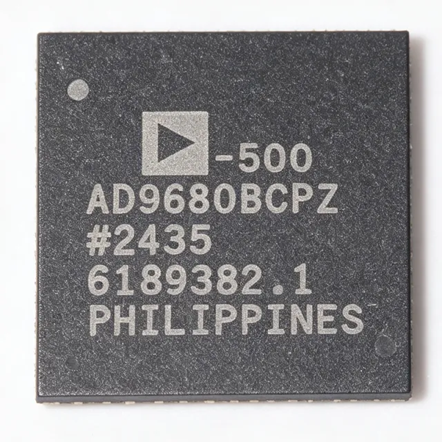
AD9680BCPZ-500 - Dual 14-Bit 500 MSPS JESD204B ADC | Analog Devices
MPN: AD9680BCPZ-500 ✓ 啟用中AD9680BCPZ-500 概覽
An analog-to-digital converter (ADC) is a mixed-signal integrated circuit that samples a continuous analog waveform and converts it into a discrete digital representation. High-speed ADCs like the AD9680 sit at the front end of the signal chain hierarchy - after amplification and filtering, and before digital processing in FPGAs or ASICs - making them critical components in any wideband data acquisition system.
Key features include a 14-bit pipelined core per channel, a JESD204B high-speed serial output that drastically reduces pin count versus parallel LVDS or CMOS interfaces, an on-chip buffer and sample-and-hold circuit designed for low power, small size, and ease of use, and fast detect outputs (FD_A and FD_B on pins 17 and 32) for channel power monitoring.
Architecturally, each channel uses a pipelined conversion topology in which the input is successively quantized by cascaded low-resolution stages, enabling 500 MSPS throughput while the integrated buffer relaxes external drive requirements. The multi-rail supply architecture (1.2 V core, 2.5 V analog) optimizes power consumption versus dynamic performance.
Typical applications include software-defined radio and military communications receivers, wideband test and measurement instrumentation, cellular basestation receivers, and radar/electronic warfare systems where dual-channel simultaneous sampling at hundreds of megahertz is required.
A key design consideration is the JESD204B link configuration and clocking architecture: a low-jitter sampling clock is essential to realize the full SNR potential of the 14-bit core, so engineers should budget jitter carefully and follow ADI reference designs for the SYSREF and device clock distribution.
This page synthesizes verified distributor data, drop-in same-family alternatives, and practical engineering design guidance not found in a single manufacturer datasheet, providing a complete selection resource in one place.
直接替換替代品,適用於 AD9680BCPZ-500 — 相同封裝,腳位對腳位相容。需重新設計 PCB 的不同封裝零件不列入。
此系列的變體
與下列產品可直接替換的同系列型號: AD9680BCPZ-500 (相同外形與佔位) — 差異在於 Package, Resolution, Sampling Rate.
快速比較工具 — 選擇替代零件進行並排比較:
AD9680BCPZ-1250
✗ 缺貨
$840 / 單位
查看資料表 →AD9680BCPZ-820
📋 參考替代品(不在目錄中)
AD9680BCPZ-1000
聯絡詢價
查看資料表 →AD9680BCPZ-500 最大額定值與電氣特性
| 解析度 | 14 bit |
| Number of Channels | 2 |
| 取樣率 | 500 MSPS |
| Architecture | Pipelined |
| 介面類型 | JESD204B Serial |
| Supply Voltage (Analog) | 2.5 V |
| Supply Voltage (Core) | 1.2 V |
| 封裝 | 64-LFCSP (9 mm x 9 mm) with exposed pad |
| 安裝類型 | Surface Mount |
| On-Chip Features | Buffer and sample-and-hold circuit |
| Fast Detect Outputs | FD_A (pin 17), FD_B (pin 32) |
| Input Configuration | Differential |
| RoHS 狀態 | Compliant |
AD9680BCPZ-500 64-lfcsp (9 mm x 9 mm) with exposed pad 腳位配置指南
AD9680BCPZ-500(64-lfcsp (9 mm x 9 mm) with exposed pad 封裝)的腳位配置。 此類比元件具有輸入、輸出與電源腳位。偏移歸零、補償與致能腳位配置請參閱製造商資料表。適用於訊號調理與放大器電路。

無詳細腳位定義資料: AD9680BCPZ-500.
請參閱 資料表 以查看完整腳位配置。
典型應用
AD9680BCPZ-500 適用於 6 應用s: Software-Defined Radio Receivers, Wideband Test and Measurement Instrumentation, Cellular Basestation Receivers, Radar and Electronic Warfare Systems, Medical Imaging Data Acquisition, FPGA-Based High-Speed Data Capture.
Software-Defined Radio Receivers
The AD9680BCPZ-500 fits SDR receiver front ends where dual 14-bit channels digitize wideband IF signals at up to 500 MSPS. Its pipelined core and on-chip buffer reduce external analog design effort, while the JESD204B output streams both channels to an FPGA over a few serial lanes instead of dozens of parallel lines. In a typical superheterodyne SDR, the converter samples a 70 MHz to 250 MHz IF after a low-jitter clock drives the SYSREF-synchronized link. The 500 MSPS rate yields a 250 MHz Nyquist band, sufficient for most tactical and commercial waveforms; the fast detect outputs flag strong in-band signals for agile filtering.
推薦
Wideband Test and Measurement Instrumentation
Digitizing oscilloscopes, spectrum analyzers, and recorders benefit from the AD9680BCPZ-500's dual simultaneous channels, which enable correlated dual-capture, interleaving studies, or differential measurement architectures. At 500 MSPS and 14 bits, the converter provides approximately 86 dB of theoretical dynamic range for capturing small signals near large carriers. The integrated sample-and-hold with on-chip buffer eases drive requirements from analog front-end amplifiers, simplifying signal-chain design in dense instruments. Because both channels share one clock domain, skew between captures is minimized, a requirement for phase-sensitive measurement and vector signal analysis applications in laboratory and production test settings.
推薦
Cellular Basestation Receivers
Multi-carrier wireless infrastructure receivers use the AD9680BCPZ-500 to digitize wideband IF signals covering multiple carriers at once. Dual channels support diversity or MIMO receive paths with a single converter, halving component count versus two single-channel ADCs. The JESD204B interface provides deterministic latency and multi-chip synchronization through SYSREF, essential for coherent carrier aggregation across multiple receive cards. At 500 MSPS the 250 MHz Nyquist band accommodates typical multi-carrier IF allocations for 4G and sub-6GHz 5G deployments. Fast detect outputs support power-aware DPD and carrier management, while the 64-LFCSP exposed-pad package suits the thermal constraints of dense remote radio unit designs.
推薦
Radar and Electronic Warfare Systems
Pulse-capture radar and EW receivers demand simultaneous dual-channel sampling with wide dynamic range, both delivered by the AD9680BCPZ-500's 14-bit 500 MSPS pipelined cores. The fast detect outputs (pins 17 and 32) implement an industry-first threshold flagging mechanism that lets system controllers react to large in-band signals before full digital processing completes - valuable for threat identification and receiver protection. JESD204B serialization keeps channel counts manageable inside conformal or man-portable form factors. Where instantaneous bandwidth beyond 250 MHz is needed for wide-open intercept receivers, the pin-compatible AD9680BCPZ-1000 or -1250 can be substituted on the same PCB footprint without redesign.
推薦
Medical Imaging Data Acquisition
Ultrasound and digital X-ray front ends leverage the AD9680BCPZ-500's dual-channel architecture to digitize pairs of transducer or detector channels with matched timing. The 14-bit resolution preserves small echo amplitudes adjacent to strong transmit leakage, and the low-noise design of the input buffer protects signal integrity in high-channel-count arrays. JESD204B output reduces the trace count routed to the imaging processing FPGA, easing layout in probe-cable-constrained designs. At 500 MSPS, sampling supports high-frequency therapeutic and ophthalmic ultrasound bands up to roughly 250 MHz Nyquist. The exposed-pad 64-LFCSP manages heat in thermally sensitive head-end assemblies close to patient interfaces.
推薦
FPGA-Based High-Speed Data Capture
The AD9680BCPZ-500 pairs directly with JESD204B-capable FPGAs such as Intel and Xilinx transceiver families for general-purpose high-speed capture cards. The serialized interface requires only a few high-speed lanes for both 14-bit channels at 500 MSPS, dramatically simplifying the PCB versus parallel buses and enabling longer, lower-cost routing between ADC and FPGA. Deterministic-latency SYSREF synchronization supports coherent multi-board systems. Designers should implement the ADI JESD204B link parameters exported over SPI and use the vendor's IP cores for link bring-up. The 64-LFCSP footprint with exposed pad simplifies ground return management under high serial lane rates on multilayer capture boards.
推薦
推薦產品摘要
工程參考資料,適用於 AD9680BCPZ-500 — 比較、設計指引及合規資訊。
選型指南
與替代品比較
| 參數 | 本產品 | AD9680BCPZ-820 | AD9680BCPZ-1000 | AD9680BCPZ-1250 |
|---|---|---|---|---|
| Package | 64-LFCSP (9x9) EP | 64-LFCSP (9x9) EP - same | 64-LFCSP (9x9) EP - same | 64-LFCSP (9x9) EP - same |
| Brand | Analog Devices | Analog Devices | Analog Devices | Analog Devices |
| Resolution | 14 bit | 14 bit | 14 bit | 14 bit |
| Channels | 2 | 2 | 2 | 2 |
| Maximum Sample Rate | 500 MSPS | 820 MSPS | 1 GSPS | 1.25 GSPS |
| Output Interface | JESD204B | JESD204B | JESD204B | JESD204B |
| Supply Voltage | 1.2 V / 2.5 V | 1.2 V / 2.5 V | 1.2 V / 2.5 V | 1.2 V / 2.5 V |
| Power Consumption | Lowest in family | Higher than -500 | Higher than -820 | Highest in family |
| Fast Detect Outputs | FD_A, FD_B (pins 17, 32) | Yes - same pins | Yes - same pins | Yes - same pins |
主要差異化特點
- Lowest power in the AD9680 family (對比AD9680BCPZ-1250)
- Identical footprint for future bandwidth upgrades (對比AD9680BCPZ-1000)
- Integrated buffer and sample-and-hold (對比Generic dual ADC solutions)
設計說明
The effective noise figure of a 14-bit 500 MSPS converter is dominated by aperture jitter of the sampling clock. For the AD9680BCPZ-500, clock jitter should be kept below roughly 100 fs RMS to preserve SNR at high analog input frequencies. Use a dedicated low-noise PLL/clock JESD204B device such as the AD9528, filter the reference, and route the sampling clock differentially, keeping clock traces away from JESD204B lanes and analog inputs to prevent coupling-induced spurs.
The 64-LFCSP exposed pad is the primary thermal and ground path. Connect the exposed pad to a solid ground plane through an array of at least 5x5 thermal vias, as recommended in the ADI datasheet layout section. Estimated: at typical dual-channel operation, power in the hundreds of milliwatts range over the small 9 mm x 9 mm body means a well-designed via array is mandatory; an inadequate pad connection raises junction temperature and degrades AC performance.
Do not treat the three supply rails as interchangeable: AVDD1, AVDD2, and AVDD3 (see datasheet pin table, pins 1-4) power different core and output domains and require independent low-noise LDO or ferrite-isolated supplies per the ADI reference designs. Additionally, JESD204B link bring-up requires correct SPI register configuration for lane rate and scrambling; consult the ADI JESD204B application note and reference design before assuming default register settings will link with your FPGA.
合規資訊
RoHS compliant and lead-free per distributor listings (DigiKey/Arrow). REACH, halogen-free, and conflict minerals status not stated in retrieved data.






