ADXL357BEZ - Low Noise 3-Axis MEMS Accelerometer | Analog Devices
MPN: ADXL357BEZ ✓ 啟用中| 數量 | 單價 | 小計 |
|---|---|---|
| 1 | $150 | $150.00 |
| 10 | $108.3333 | $1,083.33 |
| 100 | $95.8333 | $9,583.33 |
| 500 | $91.6667 | $45,833.35 |
| 1,000 | $87.5 | $87,500.00 |
ADXL357BEZ 概覽
An accelerometer is a sensor that measures proper acceleration, which is the rate of change of velocity of a body in its own instantaneous rest frame. MEMS (Micro-Electro-Mechanical Systems) accelerometers are micro-machined devices that integrate mechanical sensing elements with electronic circuitry on a single chip. They are widely used in motion sensing, vibration monitoring, and inertial navigation systems. The ADXL357BEZ belongs to the category of digital-output accelerometers, which convert the sensed acceleration into a digital signal for direct interfacing with microcontrollers or digital signal processors.
Key features of the ADXL357BEZ include ultra-low noise density of 80 µg/√Hz, low 0 g offset drift of less than 0.75 mg over temperature, and low power consumption of 200 µA at 3.3 V. The device supports both SPI and I2C digital interfaces, allowing flexible integration into various system architectures. It also includes an integrated temperature sensor and a 32-level FIFO buffer to reduce host processor loading.
The ADXL357BEZ utilizes a capacitive sensing element with a high-resolution sigma-delta ADC, providing excellent linearity and stability. The device is factory-calibrated for sensitivity and offset, minimizing the need for user calibration. Its low noise and low drift characteristics make it suitable for precision applications such as structural health monitoring, platform stabilization, and seismic sensing.
Typical applications include industrial vibration monitoring, inertial measurement units (IMUs), robotics, and aerospace navigation systems. The device's wide measurement range and high bandwidth enable it to capture both low-frequency tilt and high-frequency vibration signals. Its low power consumption makes it ideal for battery-powered wireless sensor nodes.
When designing with the ADXL357BEZ, ensure proper power supply decoupling with a 0.1 µF capacitor close to the VDD pin and a 1 µF capacitor on the VDD I/O pin. The device requires a supply voltage between 2.25 V and 3.6 V, and the digital interface voltage can be set independently via the VDD I/O pin. Careful PCB layout with a solid ground plane is recommended to minimize noise coupling.
直接替換替代品,適用於 ADXL357BEZ — 相同封裝,腳位對腳位相容。需重新設計 PCB 的不同封裝零件不列入。
此系列的變體
與下列產品可直接替換的同系列型號: ADXL357BEZ (相同外形與佔位) — 差異在於 0 g Offset Drift, Bandwidth, Interface, Measurement Range, Noise Density.
快速比較工具 — 選擇替代零件進行並排比較:
ADXL357BEZ-RL7
聯絡詢價
查看資料表 →ADXL357BCPZ
📋 參考替代品(不在目錄中)
ADXL356BEZ
📋 參考替代品(不在目錄中)
ADXL356B
📋 參考替代品(不在目錄中)
ADXL357B
📋 參考替代品(不在目錄中)
ADXL357BEZ 最大額定值與電氣特性
| 量測範圍 | ±10g, ±20g, ±40g (selectable) |
| 介面 | SPI, I2C |
| Bandwidth | 1 Hz to 1 kHz |
| 雜訊密度 | 80 µg/√Hz |
| 0 g Offset Drift | < 0.75 mg over temperature |
| 供應電壓 | 2.25 V to 3.6 V |
| Current Consumption | 200 µA at 3.3 V |
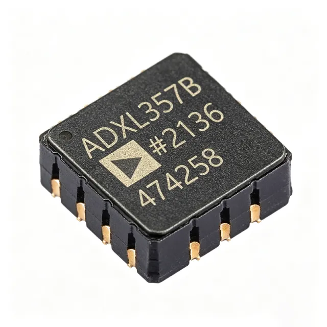
| 封裝 | 14-CLCC (6x6 mm) |
| 工作溫度 | -40°C to +125°C |
| FIFO | 32-level |
| Temperature Sensor | Integrated |
| RoHS | Compliant |
| 安裝類型 | Surface Mount |
ADXL357BEZ 腳位配置
| 腳位 1 | VDD — Power supply |
| 腳位 2 | GND — Ground |
| 腳位 3 | SCLK/SCL — SPI clock or I2C clock |
| 腳位 4 | SDI/SDA — SPI data in or I2C data |
| 腳位 5 | SDO/ADR0 — SPI data out or I2C address bit |
| 腳位 6 | CS — Chip select |
| 腳位 7 | VDD I/O — Digital interface supply |
| 腳位 8 | INT1 — Interrupt 1 |
| 腳位 9 | INT2 — Interrupt 2 |
| 腳位 10 | NC — No connect |
| 腳位 11 | NC — No connect |
| 腳位 12 | NC — No connect |
| 腳位 13 | NC — No connect |
| 腳位 14 | NC — No connect |
典型應用
ADXL357BEZ 適用於 6 應用s: Industrial Vibration Monitoring, Inertial Measurement Units (IMUs), Structural Health Monitoring, Robotics and Platform Stabilization, Seismic Sensing, Aerospace Navigation.
Industrial Vibration Monitoring
The ADXL357BEZ's low noise density of 80 µg/√Hz and wide bandwidth up to 1 kHz make it ideal for detecting subtle vibrations in industrial machinery. Its selectable ranges of ±10g, ±20g, and ±40g allow optimization for different vibration levels. The digital SPI/I2C interface simplifies integration with industrial controllers, and the low power consumption enables battery-powered wireless condition monitoring nodes. The device's low 0 g offset drift ensures stable long-term measurements, critical for predictive maintenance systems.
推薦
Inertial Measurement Units (IMUs)
The ADXL357BEZ provides the acceleration sensing core for IMUs, offering low noise and low drift essential for accurate inertial navigation. Its 3-axis measurement with selectable ranges covers various dynamic environments. The digital output simplifies data fusion with gyroscopes, and the 32-level FIFO reduces host processor load. The device's low power consumption is beneficial for portable and battery-operated IMU systems, such as those in drones and robotics.
推薦
Structural Health Monitoring
The ADXL357BEZ's low noise and low drift make it suitable for long-term structural health monitoring of bridges, buildings, and dams. Its wide bandwidth captures both static tilt and dynamic vibrations. The device's low power consumption allows deployment in remote, battery-powered sensor nodes. The digital interface enables easy data logging and analysis. The wide temperature range ensures reliable operation in outdoor environments.
推薦
Robotics and Platform Stabilization
The ADXL357BEZ provides precise acceleration feedback for robotics and platform stabilization systems. Its low noise density enables accurate motion control, while the selectable ranges accommodate different dynamic requirements. The SPI/I2C interface allows direct connection to microcontrollers, and the FIFO buffer reduces real-time processing demands. The device's small 6x6 mm CLCC package is ideal for space-constrained robotic joints and gimbals.
推薦
Seismic Sensing
The ADXL357BEZ's ultra-low noise density of 80 µg/√Hz makes it suitable for seismic sensing applications, where detecting micro-vibrations is critical. Its low drift ensures stable baseline measurements over time. The device's wide bandwidth allows capture of both low-frequency seismic waves and higher-frequency aftershocks. The digital output simplifies data acquisition, and the low power consumption enables deployment in remote seismic stations.
推薦
Aerospace Navigation
The ADXL357BEZ is used in aerospace navigation systems, including drones and UAVs, where low noise and low drift are essential for accurate inertial navigation. Its wide temperature range and robust CLCC package ensure reliability in harsh environments. The digital interface allows integration with flight controllers, and the low power consumption is critical for battery-powered aircraft. The selectable ranges accommodate various flight dynamics.
推薦
推薦產品摘要
工程參考資料,適用於 ADXL357BEZ — 比較、設計指引及合規資訊。
選型指南
與替代品比較
| 參數 | 本產品 | ADXL357BEZ-RL7 | ADXL357BCPZ | ADXL356BEZ |
|---|---|---|---|---|
| Package | 14-CLCC (6x6) | 14-CLCC (6x6) | 14-CLCC (6x6) | 14-CLCC (6x6) |
| Brand | Analog Devices | Analog Devices | Analog Devices | Analog Devices |
| Output Type | Digital (SPI/I2C) | Digital (SPI/I2C) | Digital (SPI/I2C) | Analog |
| Measurement Range | ±10g, ±20g, ±40g | ±10g, ±20g, ±40g | ±10g, ±20g, ±40g | ±10g, ±20g, ±40g |
| Noise Density | 80 µg/√Hz | 80 µg/√Hz | 80 µg/√Hz | 80 µg/√Hz |
| Supply Voltage | 2.25 V to 3.6 V | 2.25 V to 3.6 V | 2.25 V to 3.6 V | 2.25 V to 3.6 V |
| Current Consumption | 200 µA | 200 µA | 200 µA | 200 µA |
| FIFO | 32-level | 32-level | 32-level | None |
主要差異化特點
- Ultra-low noise density of 80 µg/√Hz (對比ADXL356BEZ)
- Digital SPI/I2C interface (對比ADXL356BEZ)
- 32-level FIFO buffer (對比ADXL356BEZ)
設計說明
Ensure a clean power supply for the ADXL357BEZ. Place a 0.1 µF capacitor close to the VDD pin and a 1 µF capacitor on the VDD I/O pin. The supply voltage should be between 2.25 V and 3.6 V, and the VDD I/O pin can be set independently to match the host logic level, reducing power consumption in mixed-voltage systems.
Use a solid ground plane beneath the ADXL357BEZ to minimize noise coupling. Keep the SPI/I2C traces short and shielded if possible. Avoid routing high-speed digital lines near the analog sensing elements. Follow the layout guidelines in the ADXL357 datasheet for optimal performance.
Do not exceed the absolute maximum ratings, especially on the VDD and VDD I/O pins. Ensure the digital interface voltage does not exceed the supply voltage. When using the FIFO, configure the watermark interrupt correctly to avoid data loss. Also, account for the device's power-up time before reading data.
合規資訊
RoHS compliance inferred from Analog Devices standard compliance. Other compliance data not explicitly provided.